DOI:
10.1039/C7RA11654C
(Paper)
RSC Adv., 2018,
8, 1477-1480
Decreasing graphene synthesis temperature by catalytic metal engineering and thermal processing
Received
22nd October 2017
, Accepted 24th November 2017
First published on 4th January 2018
Abstract
Chemical vapor deposition (CVD) from gaseous hydrocarbon sources has shown great promise for large-scale graphene growth, but the high growth temperature, typically 1050 °C, requires precise and expensive equipment and makes the direct deposition of graphene in electronic device manufacturing processes unfeasible due to the severe physical damage to substrates. Here we demonstrate a facile route to synthesize graphene by catalytic metal engineering and thermal processing. The engineered catalytic metal (copper) with carbon implantation could lower the synthetic temperature to 700 °C. And the resulting graphene shows few defects, uniform morphology and high carrier mobility, comparable to CVD graphene grown at 1050 °C. This technique could expand the applications of graphene in electronic and optoelectronic device manufacturing and is compatible with conventional microelectronics technology.
1. Introduction
Graphene, an atomically thin film made of honeycomb carbon atoms, has received considerable attention due to its fabulous electrical, optical and mechanical performance.1–5 The 2D planar structure of graphene makes it compatible with traditional electronic device architectures and it has been proposed for applications in frequency transistors, transparent conducting electrodes, and sensors for optical, gas, and strain detection.6–10 To date, metal-catalyzed chemical vapor deposition (CVD) by decomposition of methane has been commonly utilized to fabricate large-scale and high-quality graphene.11–15 For industrial applications, large-area and high-quality graphene is demanded at low cost. However, CVD growth of graphene is usually performed at a high temperature (i.e., 1050 °C),13–15 which requires precise and expensive equipment and makes the direct deposition of graphene in electronic device manufacturing processes infeasible due to the severe physical damage to substrates (e.g., metals, semiconductors, and the junctions between them). In order to address this issue, low temperature synthesis of graphene urgently needs to be achieved. Plasma enhanced CVD (PECVD) can effectively reduce the growth temperature, but the etching and bombarding effects of high energy hydrogen ions ionized by the plasma may introduce a high density of defects into graphene.16,17 Besides, PECVD is not suitable for industrial applications due to its high cost. Using less stable solid or liquid feedstock instead of methane is another approach for decreasing the CVD temperature of graphene growth. However, the flow of the pneumatolytic solid or liquid feedstock is difficult to control and most alternative feedstock such as benzene is hypertoxic. Therefore, low-temperature synthesis of graphene still remains a challenge.
In this work, we systematically analyze a facile approach to grow graphene by catalytic metal engineering prior thermal processing at a low temperature down to 700 °C. The catalytic metal (copper) was engineered by carbon implantation to form Cu/C alloys and the implanted carbon atoms acted as the feedstock for graphene synthesis. The as-deposited graphene shows few defects, uniform morphology and high carrier mobility, comparable to CVD graphene grown at 1050 °C. The resulting graphene by catalytic metal engineering and thermal processing could expand the applications of graphene in electronic and optoelectronic device manufacturing and was compatible with conventional microelectronics technology.
2. Experimental section
2.1. Low-temperature synthesis of graphene
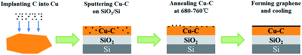
As shown in Fig. 1, the catalytic metal (Cu) was first engineered by C implanting (30 keV) and the atomic ratio of Cu and C in the obtained Cu/C alloy was 99.06![[thin space (1/6-em)]](https://www.rsc.org/images/entities/char_2009.gif) :0.04. Then Cu/C alloy was deposited on a SiO2/Si substrate by sputtering prior annealing. The annealing process was maintained at the designed temperatures (680–760 °C) for 10 min followed by naturally cooling in an annealing furnace with H2 shielding. The low content of C in the alloy was due to low solubility of C in Cu. In the alloy, C was the feedstock of graphene and Cu acted as the catalyst. Therefore, no external feedstock was needed for graphene synthesis. The thickness of Cu–C film was 1.14 μm. The design of annealing temperatures and Cu–C film thickness will be discussed in the theoretical calculation part.
:0.04. Then Cu/C alloy was deposited on a SiO2/Si substrate by sputtering prior annealing. The annealing process was maintained at the designed temperatures (680–760 °C) for 10 min followed by naturally cooling in an annealing furnace with H2 shielding. The low content of C in the alloy was due to low solubility of C in Cu. In the alloy, C was the feedstock of graphene and Cu acted as the catalyst. Therefore, no external feedstock was needed for graphene synthesis. The thickness of Cu–C film was 1.14 μm. The design of annealing temperatures and Cu–C film thickness will be discussed in the theoretical calculation part.
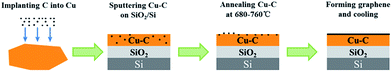 |
| | Fig. 1 The flow chart of low temperature graphene synthesis by catalytic metal engineering and thermal processing. | |
2.2. Graphene characterization
The obtained graphene films were characterized by Raman spectroscopy, atomic force microscope (AFM) and high resolution transmission electron microscopy (HRTEM), respectively. The Raman measurements were carried out using a Raman spectroscopy of HORIBA Jobin Yvon HR800. All samples were excited by Ar+ laser with wavelength of 514 nm with the spot size of 1 μm in diameter. The obtained graphene film was transferred from the Cu/SiO2/Si substrates onto glass slides by a PMMA-assisted wet-transfer method in order to directly evaluate the thickness of the graphene film. The SiO2/Si substrates were etched by 10% potassium hydroxide solution while Cu was etched by 30% iron trichloride solution. Then the cross-section microstructure of graphene on the glass was characterized by the HRTEM (JEOL-2100F). Graphene field effect transistors (GFETs) were fabricated by lithography and the device structure was detected by the scanning electron microscope (SEM) using a JEOL 7800F with an accelerating voltage of 5 kV beam. The GFETs were measured at room temperature under ambient conditions by an analytical probe station.
3. Results and discussion
3.1. Theoretical calculation
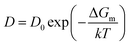
Cu–C alloys were selected as the sputtering target in which the atomic ratio of Cu and C was 99.06:0.04. The thickness of deposited Cu–C alloy could be calculated by the following equationwhere η is the copper concentration and carbon solubility (99.96/0.04), ρ is the copper atomic density (8.36 × 10²² atoms per cm3), τ is the Cu–C film thickness, and γ is the amount of carbon atoms in graphene (3.8 × 10¹⁵ atoms per cm2). Therefore, the thickness of Cu–C film could be calculated as 1.14 μm. The annealing temperature could be estimated by the following Arrhenius equation,| |
 | (2) |
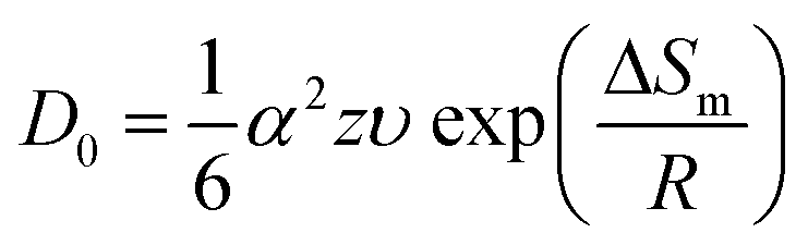
where D0 is the diffusion constant of C in Cu, ΔGm is the activation energy (0.990 eV) for the migration of the interstitial atoms, k is the Boltzmann constant, and T is the temperature. D0 can be extracted from the following equation,| |
 | (3) |
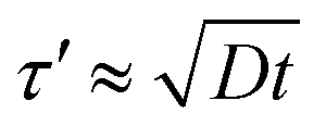
where α is the lattice constant (0.377 nm for Cu), z is the number of sites available (0.6), υ is the vibration frequency (1015 Hz), ΔSm is the entropy of migration (2.554 × 10⁴ eV K−1), and R is the gas constant (5.189 × 10¹⁹ eV K−1). As a result, D0 was estimated to be 0.14 cm2 s−1. The thickness (τ) of Cu–C film has been calculated as 1.14 μm and the distance (τ′) of carbon atoms need to travel is typically an order of magnitude greater than τ, which can be also estimated by the following equation,| |
 | (4) |
where t is the diffusion time. Assuming the diffusion time is 1 s and combining eqn (2) and (4), the annealing temperature could be estimated as 720 °C.
3.2. Synthetic temperature verification
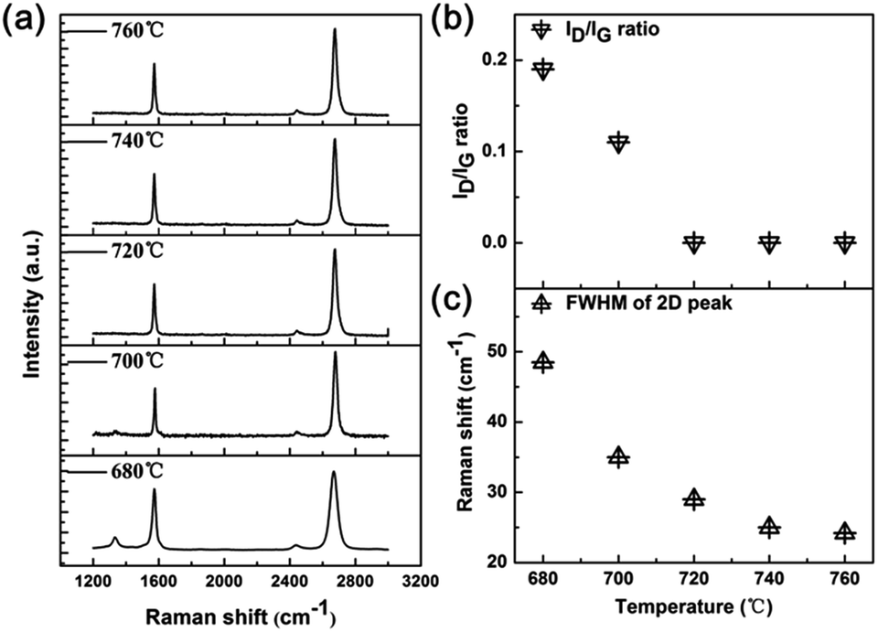
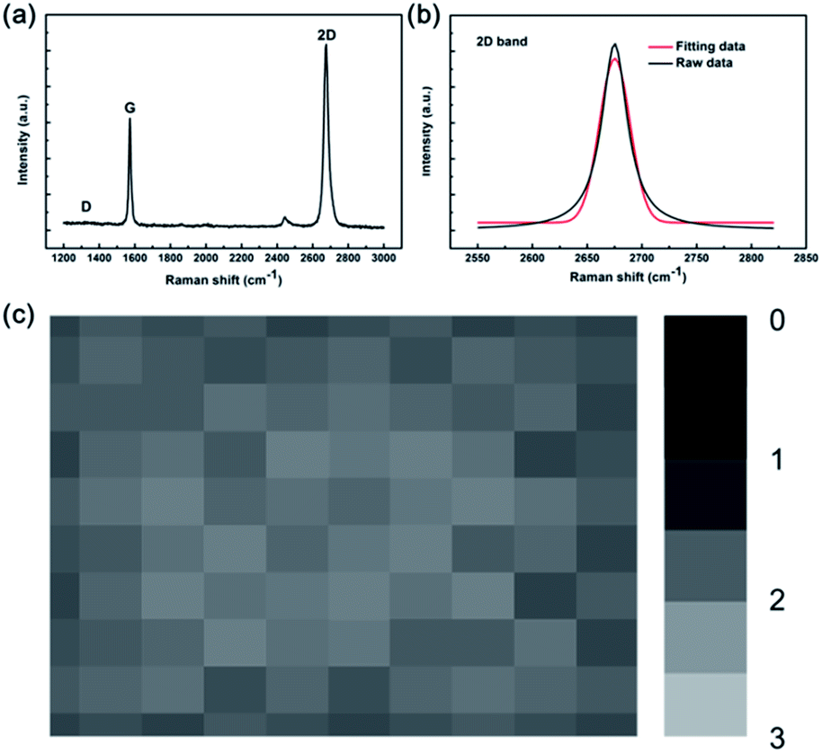
The theoretical estimation of the synthetic temperature was confirmed by experiments. Fig. 2a shows the Raman spectra of graphene by annealing Cu/C alloys at different temperatures (680–760 °C). The main features in the Raman spectrum of graphene are the G and 2D peaks, lying at around 1580 cm−1 and 2700 cm−1, respectively. The G peak corresponds to optical E2g phonons at the Brillouin zone center (Γ), whereas the 2D peak originates from a process where momentum conservation is satisfied by two phonons with opposite wave vectors.18–21 Therefore, no defects are required for the activation of 2D peak, and it thus always presents. The D peak lying at around 1300 cm−1 is due to the breathing modes of six-member rings and requires a defect for its activation.21–23 Defects, which include structural disorder such as grain boundaries or vacancies, edges, and functionalized groups, have the effect of increasing D peak intensity (ID), decreasing 2D band intensity (I2D) and broadening the 2D full width at half-maximum (FWHM). As shown in Fig. 2a and b, the intensity ratio of D peak and G peak (ID/IG ratio) rises with annealing temperature increases. When the annealing temperature increases to 700 °C, the D peak is not distinct, and when the annealing temperature increases to 720 °C, the D peak is undetectable, indicating the synthesized graphene films is in high quality comparable to that of CVD graphene grown at 1050 °C.11–15 In addition, the 2D band is symmetric and its full width at half maximum (FWHM) is down to ∼35 cm−1 when the temperature is 700 °C, which is in consistent with monolayer graphene.21 The FWHM of 2D peak can be further decreased by rising the annealing temperature (Fig. 2c).
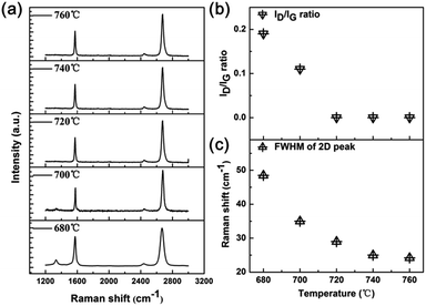 |
| | Fig. 2 (a) Raman spectra of graphene by annealing Cu/C alloys at 680–720 °C. (b) The ID/IG ratio of graphene by annealing Cu/C alloys at 680–720 °C. (c) The FWHM of 2D peak of graphene by annealing Cu/C alloys at 680–720 °C. | |
Fig. 3a depicts the representative Raman spectrum of the as-deposited graphene by annealing Cu/C alloys at 700 °C. The defect-related D band is negligible, implying that the graphene film has few defects or disorder. Furthermore, as shown in Fig. 3b, the symmetric 2D band with a FWHM of 35 cm−1 can be well fitted by a single Lorentzian curve providing evidence of monolayer graphene.21 To determine the quality, uniformity, and thickness of the graphene films deposited on a large-scale substrate, Raman mapping of the 2D to G peak intensity ratio over a 10 μm × 10 μm area with a spot size of 1 μm and a step size of 1 μm is performed, as shown in Fig. 3c. The I2D/IG ratio is quite uniform over the region investigated and the I2D/IG ratio is in the range of 1.5–2, indicating complete monolayer graphene coverage in the scanned area. Those measurements give evidence of the high crystal quality in graphene samples and indicate the graphene resultant temperature can be down to 700 °C by catalytic metal (Cu) engineering and thermal processing.
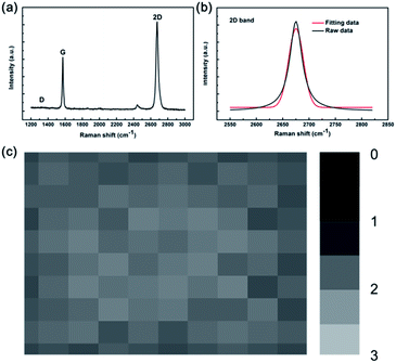 |
| | Fig. 3 (a) Raman spectrum of graphene by catalytic metal (Cu) engineering and thermal processing at 700 °C. (b) 2D band can be split into single Lorentzian curve (red curve). (c) Two-dimensional Raman mapping of the graphene film. The gradient bar to the right of each map represents the I2D/IG band ratio. | |
3.3. Characterization analysis
The surface morphology of transferred graphene on a SiO2/Si substrate has been investigated by AFM (Fig. 4a). The surface root-mean-square (RMS) roughness is down to 0.4 nm, manifesting the high uniformity and flatness of graphene deposited by catalytic metal (Cu) engineering and thermal processing. The as-deposited graphene film has also been transferred onto TEM grids by a polymethyl methacrylate (PMMA)-assisted wet-transfer method in order to directly evaluate the thickness of the graphene film as shown in Fig. 4b. The cross-section microstructure of graphene characterized by HRTEM shows its thickness is 0.3 nm, further demonstrating the as-deposited graphene is monolayer.
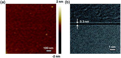 |
| | Fig. 4 (a) The AFM image of transferred graphene on a SiO2/Si substrate. (b) The HRTEM image of graphene shows its monolayer property. | |
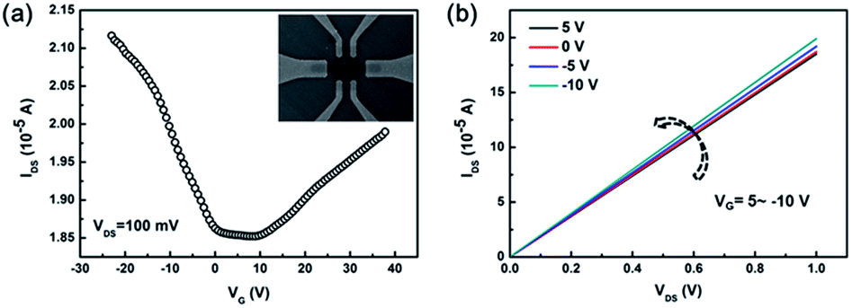
To determine the transport properties of the synthesized graphene film, the back-gated GFET has been fabricated on the SiO2 (300 nm)/Si substrates. The SEM image of GFET is shown in the inset of Fig. 5a. The highly reproducible transfer characteristics (IDS–VG) of the GFET measured at room temperature under ambient conditions is shown in Fig. 5a. The typical IDS–VG curve measured at a VDS of 100 mV shows that the gate can cause either hole or electron conduction. The V-shaped ambipolar transfer characteristic is typical of monolayer graphene with a zero bandgap.24–33 The Dirac point of the GFET shifts slightly to a positive gate at VG = 5 V, demonstrating slight p-type hole doping performance. The slight p-type doping of graphene is due to the charge transfer doping by the adsorption of atmospheric hole dopants (e.g. O2) in air.34–37 In addition, the residue of PMMA may also lead to p-type doping of graphene.37,38 According to the two slopes of the linear regions on both sides of the V-shaped curve, the hole mobility (μh) is ∼1200 cm2 V−1 s−1 and the electron mobility (μe) is ∼1100 cm2 V−1 s−1, both of which are comparable to values reported recently from transferred CVD graphene.24–33 The presence of defects, wrinkles, and overlaps generated from the transfer process may degrade the performance of GFETs, thus underestimating the carrier mobility of the synthesized graphene film. In the output characteristics of the GFET, as shown in Fig. 5b, the linear IDS–VDS behavior indicates a good ohmic contact between the Au/Ti contact and graphene channels. In addition, IDS increases with VG negative shift from 5 to −10 V and it is indicative of p-type behavior as well. The electrical transport data also reveal that the graphene deposited by catalytic metal (Cu) engineering and thermal processing is of good quality which can be further improved by refining the transfer process.
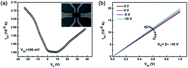 |
| | Fig. 5 (a) The IDS–VG curve of the graphene transistor at VDS = 100 mV. The inset shows the SEM image of a back-gated GFETs. (b) The IDS–VDS curves of the graphene transistor with different VG. | |
4. Conclusions
In summary, catalytic metal engineering by implanting C into Cu and thermal processing were established to deposit graphene at a low temperature down to 700 °C. Parametric studies show that the superior quality and homogeneous monolayer graphene in large scale can be directly achieved on the Cu/C substrates. Raman, AFM and HRTEM are utilized to determine both the quality and thickness of the graphene film. GFETs were designed and characterized to measure the electrical properties of the synthesized graphene film. The obtained graphene by catalytic metal engineering and thermal processing is scalable and compatible with the mainstream microelectronics technology, thus paving the way to the application of graphene in microelectronic field at a low temperature.
Conflicts of interest
There are no conflicts to declare.
Acknowledgements
This work was supported by the Shanghai Sailing Program (Grant No. 17YF1422700) and the National Scientific Foundation of Shanghai (Grant No. 16ZR1442300). We would like to thank Prof. Xiaoming Xie, Prof. Ya-Hong Xie, Prof. Zengfeng Di, A. Prof. Yan Cheng, Dr Tianbo Wang, Dr Zirui Liu, Dr Jimmy Ng, Dr Owen Liang, Dr Ming Xia, Dr Xinke Yu and Dr Zhongbo Yan for their generous help.
References
- A. K. Geim and K. S. Novoselov, Nat. Mater., 2007, 6, 183 CrossRef CAS PubMed.
- K. S. Novoselov, A. K. Geim, S. V. Morozov, D. Jiang, Y. Zhang, S. V. Dubonos, I. V. Grigorieva and A. A. Firsov, Science, 2004, 306, 666 CrossRef CAS PubMed.
- K. S. Novoselov, A. K. Geim, S. V. Morozov, D. Jiang, M. I. Katsnelson, I. V. Grigorieva, S. V. Dubonos and A. A. Firsov, Nature, 2005, 438, 197 CrossRef CAS PubMed.
- M. S. Fuhrer, Science, 2013, 340, 1413 CrossRef CAS PubMed.
- J. H. Chen, C. Jang, S. Xiao, M. Ishigami and M. S. Fuhrer, Nat. Nanotechnol., 2008, 3, 206 CrossRef CAS PubMed.
- Y.-M. Lin, C. Dimitrakopoulos, K. A. Jenkins, D. B. Farmer, H.-Y. Chiu and A. Grill, et al., Science, 2010, 323, 662 CrossRef PubMed.
- X. Li, Y. Zhu, W. Cai, M. Borysiak, B. Han and D. Chen, et al., Nano Lett., 2009, 9, 4359 CrossRef CAS PubMed.
- B. Y. Zhang, T. Liu, B. Meng, X. Li, G. Liang and X. Hu, et al., Nat. Commun., 1811, 2013, 4 Search PubMed.
- S. Basu and P. Bhattacharyya, Sens. Actuators, B, 2012, 173, 1 CrossRef CAS.
- S.-H. Pan, H. Medina, S.-B. Wang, L.-J. Chou, Z. M. Wang and K.-H. Chen, et al., Nanoscale, 2014, 6, 8635 RSC.
- Y. Wu, Y. Hao, H. Y. Jeong, Z. Lee, S. Chen and W. Jiang, et al., Adv. Mater., 2013, 25, 6744 CrossRef CAS PubMed.
- Q. Li, H. Chou, J. H. Zhong, J. Y. Liu, A. Dolocan and J. Zhang, et al., Nano Lett., 2013, 13, 486 CrossRef CAS PubMed.
- X. Li, W. Cai, L. Colombo and R. S. Ruoff, Nano Lett., 2009, 9, 4268 CrossRef CAS PubMed.
- S. Bhaviripudi, X. Jia, M. S. Dresselhaus and J. Kong, Nano Lett., 2010, 10, 4128 CrossRef CAS PubMed.
- Y. Wu, Y. Hao, H. Y. Jeong, Z. Lee, S. Chen and W. Jiang, et al., Adv. Mater., 2013, 25, 6744 CrossRef CAS PubMed.
- R. John, A. Ashokreddy, C. Vijayan and T. Pradeep, Nanotechnology, 2011, 22, 165701 CrossRef PubMed.
- L. Xie, L. Jiao and H. Dai, J. Am. Chem. Soc., 2010, 132, 14751 CrossRef CAS PubMed.
- L. Zheng, X. Cheng, D. Cao, G. Wang, Z. Wang and D. Xu, et al., ACS Appl. Mater. Interfaces, 2014, 6, 7014 CAS.
- L. Zheng, X. Cheng, D. Cao, Z. Wang, C. Xia and Y. Yu, et al., Appl. Phys. Lett., 2014, 104, 023112 CrossRef.
- D. C. Elias, R. R. Nair, T. M. G. Mohiuddin, S. V. Morozov, P. Blake and M. P. Halsall, et al., Science, 2009, 323, 610 CrossRef CAS PubMed.
- A. C. Ferrari and D. M. Basko, Nat. Nanotechnol., 2013, 8, 235 CrossRef CAS PubMed.
- A. C. Ferrari and J. Robertson, Phys. Rev. B: Condens. Matter Mater. Phys., 2000, 61, 14095 CrossRef CAS.
- K. K. Mani and R. Ramani, Phys. Status Solidi B, 1974, 61, 659 CrossRef CAS.
- V. Singh, D. Joung, L. Zhai, S. Das, S. I. Khondaker and S. Seal, Prog. Mater. Sci., 2011, 56, 1178 CrossRef CAS.
- S. Bhaviripudi, X. Jia, M. S. Dresselhaus and J. Kong, Nano Lett., 2010, 10, 4128 CrossRef CAS PubMed.
- R. John, A. Ashokreddy, C. Vijayan and T. Pradeep, Nanotechnology, 2011, 22, 165701 CrossRef PubMed.
- M. Zhu, Z. Du, Z. Yin, W. Zhou, Z. Liu and S. H. Tsang, et al., ACS Appl. Mater. Interfaces, 2016, 8, 502 CAS.
- R. Munoz and C. Gomez-Aleixandre, Chem. Vap. Deposition, 2013, 19, 297 CrossRef CAS.
- I. A. Kostogrud, K. V. Trusov and D. V. Smovzh, Adv. Mater. Interfaces, 2016, 3, 1500823 CrossRef.
- S. J. Chae, F. Güneş, K. K. Kim, E. S. Kim, G. H. Han and S. M. Kim, et al., Adv. Mater., 2009, 21, 2328 CrossRef CAS.
- V. K. Sangwan, D. Jariwala, S. A. Filippone, H. J. Karmel, J. E. Johns and J. M. Alaboson, et al., Nano Lett., 2013, 13, 1162 CrossRef CAS PubMed.
- S. K. Lee, H. Y. Jang, S. Jang, E. Choi, B. H. Hong and J. Lee, et al., Nano Lett., 2012, 12, 3472 CrossRef CAS PubMed.
- L. Wang, X. Chen, Y. Wang, Z. Wu, W. Li and Y. Han, et al., Nanoscale, 2013, 5, 1116 RSC.
- S. Ryu, L. Liu, S. Berciaud, Y. J. Yu, H. Liu and P. Kim, et al., Nano Lett., 2010, 10, 4944 CrossRef CAS PubMed.
- L. Zheng, X. Cheng, Z. Wang, C. Xia, D. Cao and L. Shen, et al., J. Phys. Chem. C, 2015, 119, 5995 CAS.
- D. W. Boukhvalov and M. I. Katsnelson, J. Phys. Chem. C, 2009, 113, 14716 Search PubMed.
- U. N. Maiti, W. J. Lee, J. M. Lee, Y. Oh, J. Y. Kim and J. E. Kim, et al., Adv. Mater., 2014, 26, 40 CrossRef CAS PubMed.
- W. J. Yu, L. Liao, S. H. Chae, Y. H. Lee and X. Duan, Nano Lett., 2011, 11, 4759 CrossRef CAS PubMed.
|
| This journal is © The Royal Society of Chemistry 2018 |
Click here to see how this site uses Cookies. View our privacy policy here. 
 Open Access Article
 This Open Access Article is licensed under a Creative Commons Attribution-Non Commercial 3.0 Unported Licence
 *ab,
Xinhong Cheng*a,
Peiyi Yec,
Lingyan Shena,
Qian Wang
*ab,
Xinhong Cheng*a,
Peiyi Yec,
Lingyan Shena,
Qian Wang