
 Open Access Article
 This Open Access Article is licensed under a
 Creative Commons Attribution 3.0 Unported Licence
Anti-site defect effect on the electronic structure of a Bi2Te3 topological insulator
Pei-Yu Chuanga,
Shu-Hsuan Su*a,
Cheong-Wei Chonga,
Yi-Fan Chena,
Yu-Heng Choua,
Jung-Chun-Andrew Huang *abc,
Wei-Chuan Chend,
Cheng-Maw Cheng*d,
Ku-Ding Tsueid,
Chia-Hsin Wangd,
Yaw-Wen Yangd,
Yen-Fa Liaod,
Shih-Chang Wengd,
Jyh-Fu Leed,
Yi-Kang Lane,
Shen-Lin Changf,
Chi-Hsuan Leeg,
Chih-Kai Yangg,
Hai-Lin Suh and
Yu-Cheng Wuh
*abc,
Wei-Chuan Chend,
Cheng-Maw Cheng*d,
Ku-Ding Tsueid,
Chia-Hsin Wangd,
Yaw-Wen Yangd,
Yen-Fa Liaod,
Shih-Chang Wengd,
Jyh-Fu Leed,
Yi-Kang Lane,
Shen-Lin Changf,
Chi-Hsuan Leeg,
Chih-Kai Yangg,
Hai-Lin Suh and
Yu-Cheng Wuh
aDepartment of Physics, National Cheng Kung University, Tainan 701, Taiwan. E-mail: jcahuang@mail.ncku.edu.tw; macg0510@yahoo.com.tw
bAdvanced Optoelectronic Technology Center, National Cheng Kung University, Tainan 701, Taiwan
cTaiwan Consortium of Emergent Crystalline Materials, Ministry of Science and Technology, Taipei 106, Taiwan
dNational Synchrotron Radiation Research Center, Hsinchu 300, Taiwan. E-mail: makalu@nsrrc.org.tw
eMaterials and Electro-Optic Research Division, National Chung-Shan Institute of Science and Technology, Taoyuan 325, Taiwan
fDepartment of Electrophysics, National Chiao Tung University, Hsinchu 300, Taiwan
gGraduate Institute of Applied Physics, National Chengchi University, Taipei 116, Taiwan
hSchool of Materials Science and Engineering, Anhui Provincial Key Laboratory of Advanced Functional Materials and Devices, Hefei University of Technology, Hefei 230009, People's Republic of China
First published on 2nd January 2018
Abstract
Tuning the Fermi level (EF) in Bi2Te3 topological-insulator (TI) films is demonstrated on controlling the temperature of growth with molecular-beam epitaxy (MBE). Angle-resolved photoemission spectra (ARPES) reveal that EF of Bi2Te3 thin films shifts systematically with the growth temperature (Tg). The key role that a Bi-on-Te(1) (BiTe1) antisite defect plays in the electronic structure is identified through extended X-ray-absorption fine-structure (EXAFS) spectra at the Bi L3-edge. Calculations of electronic structure support the results of fitting the EXAFS, indicating that the variation of EF is due to the formation and suppression of BiTe1 that is tunable with the growth temperature. Our findings provide not only insight into the correlation between the defect structure and electronic properties but also a simple route to control the intrinsic topological surface states, which could be useful for applications in TI-based advanced electronic and spintronic devices.
1. Introduction
Topological insulators (TI) are novel quantum materials with promising applications in advanced spintronic devices. A three-dimensional (3D) TI is a gapped bulk insulator, but possesses gapless conducting surface states.1,2 These topological surface states in 3D TI arise from a band inversion of the valence and conduction bands due to strong spin–orbit interactions.3,4 This inversion makes the surface state topologically nontrivial, being protected by the time-reversal symmetry. The surface state in 3D TI shows a helical Dirac-type dispersion, in which the spin is tightly coupled to the momentum, so called spin-momentum locking.5 V2–VI3-type 3D TIs, such as Bi2Se3, Bi2Te3 and Sb2Te3, have been theoretically predicted and experimentally confirmed.4,6,7 Bi2Te3 belongs to the V2–VI3 TI family and has a rhombohedral crystal structure that can be considered to consist of the stacking of –Te(1)–Bi–Te(2)–Bi–Te(1)– quintiple layers (QL).8 Within a QL unit, the interaction between Bi and Te is a chemical force whereas the interaction between two QL involves a van der Waals force. The surface states of Bi-based TI families are widely regarded as ideal systems for applications in spintronic and quantum devices, but a large bulk charge-carrier contribution generally originates from intrinsic defects, such as anion vacancies and antisite defects in Bi-based TI.9 When the charge carrier is dominated by bulk donors, the Dirac point (DP) is located deep below the Fermi level, making it difficult to utilize the unique property of the topological surface states. Understanding and manipulating the electronic structure during the growth of a thin film of TI becomes a crucial problem, especially for the effect of key parameters such as the growth temperature on the electronic structure of TI.For a Bi2Te3 single crystal near the solid–liquid equilibrium composition for Te ranging from 58 to 62.8 atomic per cent, a substitution of Bi for a Te(1) site (BiTe1) is energetically favored and hole charge carriers dominate. In contrast, electron carriers dominate the behavior in the case of substitution of Te for Bi (TeBi) for Te in a range from 62.8 to 66 atomic per cent. For single-crystalline Bi2Te3, the p-type and n-type charge-carrier concentration can range from 3 × 10¹⁷ to 5 × 1019 cm−3, depending on the initial growth condition with excess either Bi or Te.10–14 For bulk Bi2Te3 crystal growth near the solid–liquid equilibrium temperature, anti-site defects can be simply described by element compositions. In comparison, thin film growth is far from the equilibrium conditions, so that the composition of Bi/Te can be tuned by growth temperature. In the present work, we report a systematic study of the crystal structure and electronic properties of epitaxial Bi2Te3 films upon tuning the growth temperature. A correlation between the position of the Dirac point of Bi2Te3 films via angle-resolved photoemission spectra (ARPES) and the coordination number of Bi–BiTe1 via extended X-ray-absorption fine structure (EXAFS) spectra is clearly identified. To compare with the experimental results, we conducted a simulation on BiTe and TeBi antisite defects with density-functional theory (DFT); the results support the conclusion that the variation of the electronic structure of Bi2Te3 films is highly correlated with the antisite defects that vary with the growth temperature. Our findings provide also a simple route to manipulate the Dirac point and topological surface states that can yield applications in electronic and spintronic devices.
2. Experimental
2.1 Sample preparation
The TI films were grown on c-plane Al2O3(0001) substrates with a MBE system (AdNaNo Corporation, model MBE-9). The sapphire substrates were chemically cleaned with standard procedures before being loaded into the growth chamber. To remove any possible contaminant from the surface, we heated the sapphire substrates to 1000 °C for 1 h under a ultrahigh-vacuum (UHV) environment. Highly pure Bi (99.99%) and Te (99.999%) were evaporated from Knudsen cells; the flux rate was calibrated in situ with a quartz crystal microbalance. The base pressure of the MBE system was less than 2 × 10⁻¹⁰ Torr; the pressure during growth was kept below 1 × 10⁻⁹ Torr. The Bi2Te3 thin films were prepared with a stable beam-flux ratio Te/Bi (ΦTe/Bi) ∼ 15; the substrate temperature was varied from 310 °C to 430 °C. The crystallinity of Bi2Te3 films was monitored in situ with reflection high-energy diffraction (RHEED); additional structural characterization was performed with X-ray diffraction (XRD).2.2 XPS and ARPES characterization
The stoichiometry and electronic structure of the Bi2Te3 films were characterized with X-ray photoemission spectra (XPS) and ARPES. The XPS and ARPES experiments were conducted at beamlines 24A and 21B1 at Taiwan Light Source in National Synchrotron Radiation Research Center. The MBE-grown Bi2Te3 films with a Te capping layer of thickness ∼20 Å were annealed at 260 °C about 1 h in an UHV environment to remove the capping layer before XPS and ARPES measurements. XPS were recorded with an energy analyzer (SPEC Phoiboss150); the core levels of Bi 4f and Te 3d were recorded with photon energy 800 eV. The incident photon energy for XPS measurements was calibrated with Au 4f levels. ARPES were recorded for samples in an UHV chamber equipped with a hemispherical analyzer (Scienta R4000, collection angle ±15°). The ARPES were recorded for samples at 83 K, base pressure 5 × 10⁻¹¹ Torr and photon energy 22 eV; the angular resolution was 0.2° and overall energy resolution was better than 12 meV. The position of the Dirac point was determined from an analysis of momentum distribution curves (MDC).2.3 EXAFS characterization
The local structure of Bi2Te3 thin films was determined with EXAFS spectra. The L3-edge spectra of Bi (13![[thin space (1/6-em)]](https://www.rsc.org/images/entities/char_2009.gif) 419 eV) were recorded near 296 K at beamline 07 A of NSRRC and Taiwan beamline SP12B2 of SPring-8. The fluorescence mode was implemented with the beam incident at 54.7° with respect to the sample plane; the signal was collected with a Lytle detector. The measured energy resolution of the used double-crystal Si(111) monochromator was better than 0.6 eV.
419 eV) were recorded near 296 K at beamline 07 A of NSRRC and Taiwan beamline SP12B2 of SPring-8. The fluorescence mode was implemented with the beam incident at 54.7° with respect to the sample plane; the signal was collected with a Lytle detector. The measured energy resolution of the used double-crystal Si(111) monochromator was better than 0.6 eV.
2.4 Computational
In this work we used spin-polarized density-functional calculations as implemented in the Vienna ab initio simulation package (VASP)15,16 to derive the electronic band structure. The local-density approximation was selected for the exchange–correlation potential including spin–orbit interaction (SOI). The electron–ion interaction was represented by the projector-augmented wave potential.17 The cutoff energy for the expansion of wave functions and potentials in the plane-wave basis was chosen to be 300 eV. A 9 × 9 × 1 sampling of k points in the first Brillouin zone was adopted. A vacuum space in the supercell was allocated on setting a minimum height 15 Å above the film in the cell, which was proved to be sufficient to minimize artificial interactions between supercells.3. Results and discussion
Fig. 1 depicts the XRD pattern of the MBE-grown Bi2Te3 films at substrate temperature Tg ranging from 310 °C to 430 °C. For the films grown at lower substrate temperature of Tg = 310 °C, the (015) lattice plane that can be attributed to the rhombohedral Bi2Te3 structure is also observed.18 The main feature of the XRD patterns of these Bi2Te3 samples is clearly close to that of Bi2Te3 (0001) single crystal.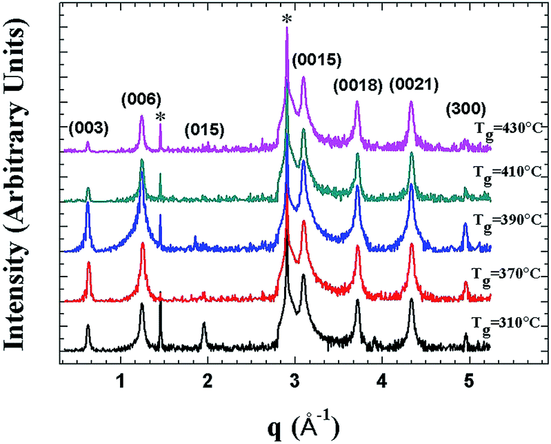 | ||
| Fig. 1 XRD curves of several Bi2Te3 epilayers grown with MBE at substrate temperature Tg from 310 to 430 °C. In this Tg range, XRD curves of Bi2Te3 samples clearly show features related to a single-crystal Bi2Te3 epilayer that is (0001)-oriented on the sapphire (0001) substrate (indicated by *). | ||
ARPES were measured to probe the quality and electronic structure of MBE-grown Bi2Te3 films. Fig. 2 shows the band structure recorded along direction Γ–K. In addition to the broad M-shaped valence-band (VB) feature located at binding energy 0.3 eV, a linear band dispersion associated with the topological surface state (TSS) was clearly observed in each sample. ARPES in a series in Fig. 2(a)–(d) show that the Fermi level varied with the growth temperature, Tg. At Tg = 310 °C, the Dirac point is located at the binding energy (EB) = −0.320 eV; the bottom of the conduction band appears below the Fermi level. On increasing Tg to 370 °C and 390 °C, the position of the Dirac point shifted to EB = −0.305 eV and −0.295 eV, respectively. A similar tendency of the position variation of the Dirac point with increasing Tg below 400 °C was reported by Guang Wang et al.,19 but when Tg was further increased to 410 °C and 430 °C, we observed an opposite trend in which the position of the Dirac point shifted further to EB = −0.315 eV and −0.335 eV, respectively. The ARPES result shows a turning point of the position of the Dirac point that occurred at Tg ∼ 390 °C. As EF was located above DP for all samples, the result indicates that the charge carriers of the Bi2Te3 films were dominantly n-type so that EF became tunable on varying growth temperature Tg.
 | ||
| Fig. 2 Band structure of Bi2Te3 at various Tg: (a) 310 °C (DP = −0.32 eV). (b) 370 °C (DP = −0.305 eV). (c) 390 °C (DP = −0.295 eV). (d) 410 °C (DP = −0.315 eV). (e) 430 °C (DP = −0.335 eV). All spectra were recorded along the Γ–K direction. The panels show the ARPES intensity maps. The surface states, valence band and conduction band of the bulk states are denoted SS, VB and CB, respectively. | ||
Hole-dominated carriers with EF located within the bandgap is expected if the electronic structure were determined mainly by the antisite defects in Bi2Te3, but the film growth occurred far from the equilibrium growth conditions of a bulk single crystal. The formation of Te vacancies can hence not be avoided during the growth of a Bi2Te3 film. Te vacancies likely provide n-type carriers as the majority carriers for all Bi2Te3 films. It is difficult to perform quantitative analysis on the Te vacancies although they play an important role in the electronic structure. Besides point defects in Bi2Te3, antisite defects, substitutional Bi on Te site (BiTe) or substitutional Te on Bi site (TeBi) are energetically favored.10,20,21 The tendency of Fermi level shift in the Bi2Te3 films observed by ARPES suggests the major defects are Te vacancies and/or BiTe. Note that the Te vacancies acts as double donors while the BiTe as triple acceptors. Therefore, n-type behavior in the Bi2Te3 films can be attributed to Te vacancies that donate electrons to the conduction band.22,23 This is consistent with the ARPES observation that the positions of the Fermi level are close to the conduction band. However, the ARPES data show clearly that EF varies with growth temperature Tg, which indicates that antisite defects also play a role in this case. According to the previous reports,19,24 a shift of the Fermi level in Bi2Te3 depends strongly on the native point of antisite defects (BiTe and TeBi) in the Bi–Te compound. Near a stoichiometric Bi2Te3 with Te fraction about 62.8 at%, acceptor-like BiTe antisite defects can dominate the carrier behavior. Donor-like TeBi antisite defects are energetically favored at a larger Te composition, above 63%. The ratio of Bi and Te can be estimated qualitatively from XPS measurements with a peak analysis of the core level spectra of Bi 4f and Te 3d; the secondary electron background is removed with the Shirley background subtraction, as shown in Fig. 3(a) and (b).25–28
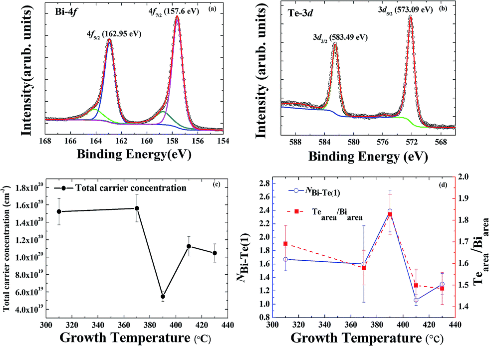 | ||
| Fig. 3 XPS of (a) Bi-4f core-level spectra and (b) Te-3d core-level spectra of the Bi2Te3 thin film grown at 390 °C. (c) Total carrier concentration of the Bi2Te3 films as a function of the growth temperature measured by Hall measurement. (d) The Te/Bi ratio of the Bi2Te3 thin films as a function of the growth temperature. | ||
The tendency that the Fermi level shifted toward the Dirac point in APRES as Tg increased from 310 to 390 °C implies that the concentration of BiTe antisite defects increased with increasing Tg, as shown in Fig. 3(d). The highest Te fraction at 390 °C as revealed in XPS might indicate the diffusion of Te atoms towards the outermost surface. The reduction of Te fraction at Tg >390 °C can be attributed to the desorption of Te from the surface.29 Nevertheless, a shift of EF away from the DP at Tg > 390 °C indicates a redistribution of the BiTe/TeBi ratio at the elevated growth temperatures. Detailed studies regarding the antisite defects dependent on growth temperature enable a quantitative analysis with EXAFS in the following.
To verify our deductions about the antisite defects, we performed Fourier transformation of the X-ray absorption spectra (XAS) at the Bi-L3 edge; the radial distribution function is shown in Fig. 4(a). The fitted results of extended X-ray-absorption fine-structure (EXAFS) spectra enable a direct identification of the antisite defects in Bi2Te3 films. In this EXAFS work we took Bi instead of Te as the central atom, because the two Te sites in each unit cell make the analysis difficult. Herein, EXAFS spectra were recorded with the background subtraction of the XAS data μ(E) and conversion of μ(E) to χ(k); both processes were performed with ATHENA using the IFEFFIT XAS package.30 The Fourier transforms (FT) of k-weighted EXAFS spectra use Hann windows with k ranging from 1.2 to 10 Å−1, as shown in Fig. 4(b). The rhombohedral primitive and hexagonal unit cell of Bi2Te3 consists of a five-layer lamellar structure of one quintuple layer (QL). The schematic diagram in Fig. 4(c) shows that a –Te(1)–Bi–Te(2)–Bi–Te(1)– five-layer structure; one Bi atom coordinates three Te atoms at each Te site. According to calculations that provided predictions for the Bi-rich condition, BiTe1 has the least formation energy, 0.4 eV and 0.9 eV, which is less than for BiTe2 and TeBi, respectively. For a Te-rich condition, TeBi has the least formation energy, 0.7 eV and 1.1 eV, which is less than for BiTe1 and BiTe2, respectively.23 The coordination relevant for Bi and Te(1) and the bond length of quantitative analysis is indicated in Table 1. At growth temperatures Tg = 310, 370 and 390 °C, the coordination numbers of Bi–BiTe1 (NBi–BiTe1) that correspond to the substitution of Bi for Te(1) are 1.05 ± 0.11, 1.312 ± 0.47 and 2.725 ± 0.35, respectively. Accordingly, the length of the Bi–Te(1) bond decreased to 3.04 ± 0.31 Å, 3.02 ± 1.07 Å, and 2.88 ± 0.37 Å, as more Te(1) sites became occupied with Bi atoms. When the growth temperature exceeded 390 °C, the coordination number of Bi–BiTe1 (NBi–BiTe1) decreased to 0.77 ± 0.06 at Tg = 410 °C. Moreover, no Bi substitution was observed at Tg = 430 °C. The length of the Bi–Te(1) bond increased to 3.06 ± 0.23 Å and 3.04 ± 0.36 Å at Tg = 410 and 430 °C respectively.
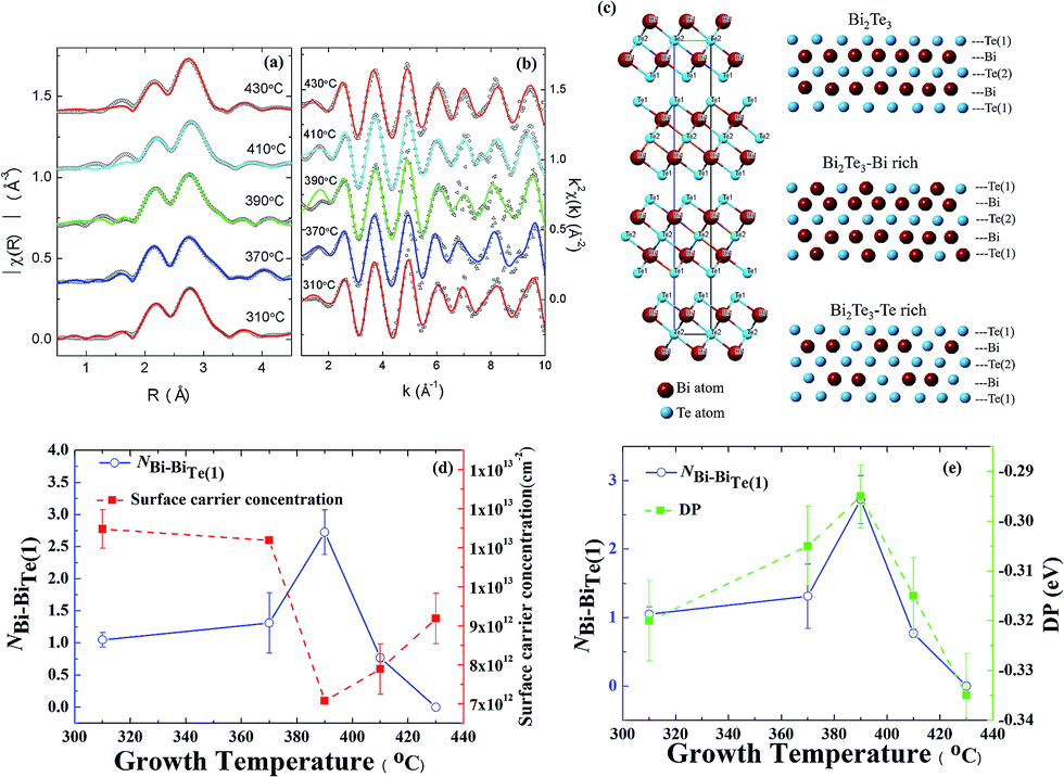 | ||
| Fig. 4 EXAFS spectra at the Bi L3-edge of the Bi2Te3 thin films. The curves are vertically shifted for the substrate temperature. (a) Fourier transform of the R-space (symbols) together with the theoretical fit to the first shells (solid line). (b) k-Space (symbols) together with the best fit (solid line). (c) Hexagonal conventional unit cells of Bi2Te3; schematic diagram of one QL of the mechanism of the antisite defect in Bi-rich and Te-rich conditions, respectively. (d) BiTe antisite of Bi–Bi averaged coordination number and surface carrier concentration (estimated from the Fermi level crossing kF) plotted versus Tg. (e) BiTe antisite of Bi–Bi averaged coordination number and Dirac point at binding energy plotted versus Tg. | ||
| Sample | NBi–Te1 | BLBi–Te1 (Å) | NBi–BiTe1 | BLBi–BiTe1 (Å) |
|---|---|---|---|---|
| Tg = 310 °C | 1.67 ± 0.17 | 3.04 ± 0.31 | 1.05 ± 0.11 | 3.13 ± 0.32 |
| Tg = 370 °C | 1.6 ± 0.57 | 3.02 ± 1.07 | 1.312 ± 0.47 | 3.11 ± 1.1 |
| Tg = 390 °C | 2.39 ± 0.31 | 2.88 ± 0.37 | 2.725 ± 0.35 | 3.11 ± 0.4 |
| Tg = 410 °C | 1.06 ± 0.08 | 3.06 ± 0.23 | 0.77 ± 0.06 | 3.17 ± 0.24 |
| Tg = 430 °C | 1.3 ± 0.16 | 3.04 ± 0.36 | None | None |
On increasing growth temperature Tg to 390 °C, the fitted results of EXAFS clearly show the substitution of a Te(1) site by a Bi atom with increased coordination number of Bi–BiTe1. Because of the extra holes created from antisite BiTe, a smaller Fermi level crossing kF was observed from ARPES,31 indicating a decreased concentration of electron carriers. For a growth temperature above Tg = 390 °C, the coordination number of Bi–BiTe1 decreased, accompanied with an incremented concentration of electron carriers as shown in Fig. 4(d). The evolution of the DP (EF) as a function of growth temperature Tg exhibits a trend similar to that of the coordination number of Bi–BiTe1, as displayed in Fig. 4(e). Both the Tg-dependent DP and Bi–BiTe1 coincide with the variation in the concentration of electron carriers.
To confirm the above experimental studies and analyses, we calculated the electronic band structure of Bi2Te3 considering varied chemical composition. Four quintuple layers of pristine Bi2Te3 were used; one Te in the structure was replaced with a Bi atom and vice versa. The concentration of Bi was increased from 40% to 41.7% (Bi23Te37) in the former case and decreased from 40% to 38.3% in the latter. Drawn in Fig. 5(a) is the band structure of the pristine Bi2Te3 with red circles representing the contribution of the surface states of Bi2Te3. Fig. 5(b) shows the energy bands for the Bi-rich structure, with its Dirac point shifting upward in energy. In Fig. 5(c), however, the Dirac point in the Te-rich structure shifts downward in energy. The calculated energy-band structures are consistent with the Tg-dependent DP (EF) and Bi–BiTe1. As Fig. 5(d) shows, the formation of Bi–Te(1) produces a shift of the EF towards the maximum of valence band. With decreased substitution of Bi in Te(1), TeBi became the dominant defects, resulting in an increased concentration of electron carriers so that the EF shifted away from the maximum of valence band.
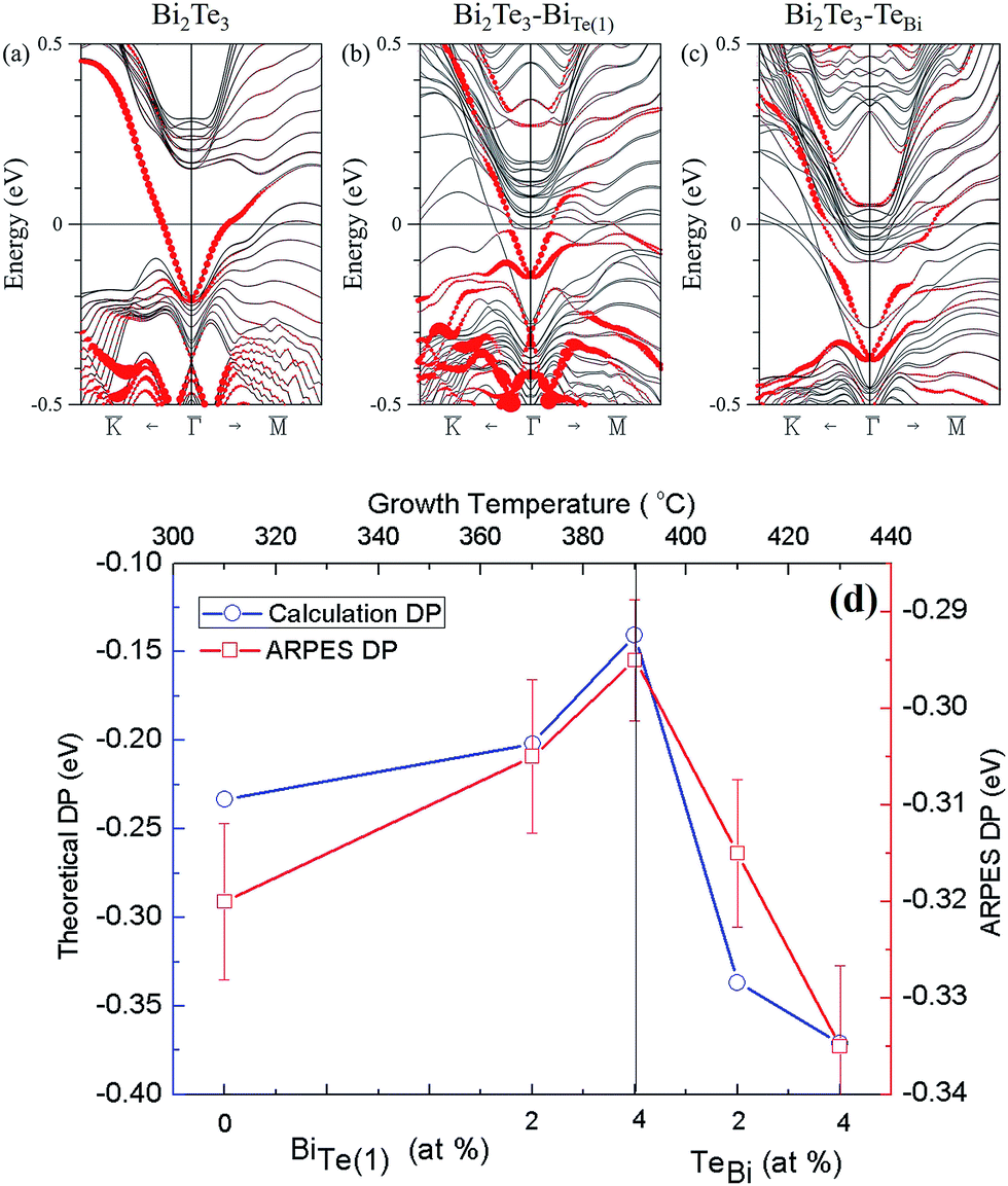 | ||
| Fig. 5 Band structure of Bi2Te3 from calculations of electronic structure for Bi-rich and Te-rich conditions. The direct coordinates of high symmetry points in the Brillouin zone are K, Γ and M as the Dirac point of Bi2Te3. (a) Electronic structure of four quintuple layers of pristine Bi2Te3 near the Γ point. The band structure is shown with (b) replacement of one Bi atom with a Te atom and (c) replacement of one Te atom with a Bi atom in 4 QL Bi2Te3. The size of the red circle indicates a contribution of the surface state in the low-energy band structure. (d) Theoretical Dirac points with Bi-rich and Te-rich antisite defect concentrations are compared with the ARPES-measured Dirac points. | ||
4. Conclusions
On controlling the growth temperature using a MBE method, we fabricated Bi2Te3 TI thin films with a varied Fermi level. ARPES and EXAFS results reveal direct evidence for the substitution of Bi for the Te(1) site, which is the key origin for the shift of the Fermi level or the position of the Dirac point in Bi2Te3. Calculations of the electronic structure support these experiments. The calculated structure of the energy band that took into account the existence of BiTe and TeBi antisite defects with Bi-rich and Te-rich conditions further revealed that the variation of the electronic structure in Bi2Te3 films can be attributed to the antisite defects that are tunable with the growth temperature. Our approaches and results demonstrated the growth of homogenous n-type Bi2Te3 films, showing the potential for topological insulator-based device applications.Author contributions
S. H. Su, C. W. Chong and J. C. A. Huang designed and prepared the experiment. P. Y. Chuang, W. C. Chen, C.-M. Cheng and K.-D. Tsuei performed ARPES measurements. The thin-film growth was performed by Y. F. Chen, Y. H. Chou, and P. Y. Chuang, for C.-H. Wang, Y. F. Liao, S. C. Weng, J. F. Lee, and Y.-W. Yang characterized samples with XPS and EXAFS. Y. K. Lan, S. L. Chang, C. H. Lee, C. K. Yang provided theoretical support. All authors have given approval to the final version of the manuscript.Conflicts of interest
There are no conflicts to declare.Acknowledgements
Ministry of Science and Technology Republic of China, Taiwan supported this research under contract MOST 103-2119-M-006-015 and 105-2112-M-213-006-MY2. Funding was received also from the headquarters of University Advancement at NCKU, which is sponsored by the Ministry of Education, Taiwan ROC. The National Synchrotron Radiation Research Center (NSRRC) is operated under the Ministry of Science and Technology of Taiwan.References
- J. E. Moore, Nature, 2010, 464, 194–198 CrossRef CAS PubMed.
- X.-L. Qi and S.-C. Zhang, Rev. Mod. Phys., 2011, 83, 1057–1110 CrossRef CAS.
- B. A. Bernevig, T. L. Hughes and S.-C. Zhang, Science, 2006, 314, 1757–1761 CrossRef CAS PubMed.
- H. Zhang, C.-X. Liu, X.-L. Qi, X. Dai, Z. Fang and S.-C. Zhang, Nat. Phys., 2009, 5, 438–442 CrossRef CAS.
- M. Z. Hasan and C. L. Kane, Rev. Mod. Phys., 2010, 82, 3045–3067 CrossRef CAS.
- Y. Xia, D. Qian, D. Hsieh, L. Wray, A. Pal, H. Lin, A. Bansil, D. Grauer, Y. S. Hor, R. J. Cava and M. Z. Hasan, Nat. Phys., 2009, 5, 398–402 CrossRef CAS.
- Y. L. Chen, J. G. Analytis, J.-H. Chu, Z. K. Liu, S. K. Mo, X. L. Qi, H. J. Zhang, D. H. Lu, X. Dai, Z. Fang, S. C. Zhang, I. R. Fisher, Z. Hussain and Z.-X. Shen, Science, 2009, 325, 178–181 CrossRef CAS PubMed.
- A. Mzerd, D. Sayah, J. C. Tedenac and A. Boyer, J. Cryst. Growth, 1994, 140, 365–369 CrossRef CAS.
- D. Hsieh, Y. Xia, D. Qian, L. Wray, J. H. Dil, F. Meier, J. Osterwalder, L. Patthey, J. G. Checkelsky, N. P. Ong, A. V. Fedorov, H. Lin, A. Bansil, D. Grauer, Y. S. Hor, R. J. Cava and M. Z. Hasan, Nature, 2009, 460, 1101–1105 CrossRef CAS PubMed.
- G. R. Miller and C.-Y. Li, J. Phys. Chem. Solids, 1965, 26, 173–177 CrossRef CAS.
- R. F. Brebrick, J. Phys. Chem. Solids, 1969, 30, 719–731 CrossRef CAS.
- C. B. Satterthwaite and R. W. Ure Jr, Phys. Rev., 1957, 108, 1164–1170 CrossRef CAS.
- H. Zou, D. M. Rowe and G. Min, J. Cryst. Growth, 2001, 222, 82–87 CrossRef CAS.
- H. Zou, D. M. Rowe and S. G. K. Williams, Thin Solid Films, 2002, 408, 270–274 CrossRef CAS.
- G. Kresse and J. Hafner, Phys. Rev. B: Condens. Matter Mater. Phys., 1993, 48, 13115–13118 CrossRef CAS.
- G. Kresse and J. Furthmiiller, Comput. Mater. Sci., 1996, 6, 15–50 CrossRef CAS.
- G. Kresse and D. Joubert, Phys. Rev. B: Condens. Matter Mater. Phys., 1999, 59, 1758–1775 CrossRef CAS.
- D. H. Kim, E. Byon, G. H. Lee and S. Cho, Thin Solid Films, 2006, 510, 148–153 CrossRef CAS.
- G. Wang, X.-G. Zhu, Y.-Y. Sun, Y.-Y. Li, T. Zhang, J. Wen, X. Chen, K. He, L.-L. Wang, X.-C. Ma, J.-F. Jia, S. B. Zhang and Q.-K. Xue, Adv. Mater., 2011, 23, 2929–2932 CrossRef CAS PubMed.
- A. Hashibon and C. Elsässer, Phys. Rev. B: Condens. Matter Mater. Phys., 2011, 84, 144117 CrossRef.
- D. O. Scanlon, P. D. C. King, R. P. Singh, A. de la Torre, S. McKeown Walker, G. Balakrishnan, F. Baumberger and C. R. A. Catlow, Adv. Mater., 2012, 24, 2154–2158 CrossRef CAS PubMed.
- P. Pecheur and G. Toussaint, J. Phys. Chem. Solids, 1994, 55(4), 327–338 CrossRef CAS.
- S. X. Zhang, L. Yan, J. Qi, M. Zhuo, Y.-Q. Wang, R. P. Prasankumar, Q. X. Jia and S. T. Picraux, Thin Solid Films, 2012, 520, 6459–6462 CrossRef CAS.
- S. Cho, Y. Kim, A. DiVenere, G. K. Wong and J. B. Ketterson, Appl. Phys. Lett., 1999, 75, 1401–1403 CrossRef CAS.
- D. A. Shirley, Phys. Rev. B: Solid State, 1972, 5, 4709–4714 CrossRef.
- M. C. Burrell and N. R. Armstrong, Appl. Surf. Sci., 1983, 17, 53–69 CrossRef CAS.
- H. E. Bishop, Surf. Interface Anal., 1981, 3, 272–274 CrossRef CAS.
- S. Tougaard, J. Electron Spectrosc. Relat. Phenom., 1999, 52, 243–271 CrossRef.
- K. Schouteden, K. Govaerts, J. Debehets, U. Thupakula, T. Chen, Z. Li, A. Netsou, F. Song, D. Lamoen, C. V. Haesendonck, B. Partoens and K. Park, ACS Nano, 2016, 10(9), 8778–8787 CrossRef CAS PubMed.
- B. Ravel and M. Newville, J. Synchrotron Radiat., 2005, 12, 537–541 CrossRef CAS PubMed.
- C. W. Luo, H. J. Wang, S. A. Ku, H.-J. Chen, T. T. Yeh, J.-Y. Lin, K. H. Wu, J. Y. Juang, B. L. Young, T. Kobayashi, C.-M. Cheng, C.-H. Chen, K.-D. Tsuei, R. Sankar, F. C. Chou, K. A. Kokh, O. E. Tereshchenko, E. V. Chulkov, Y. M. Andreev and G. D. Gu, Nano Lett., 2013, 5797–5802 CrossRef CAS PubMed.
| This journal is © The Royal Society of Chemistry 2018 |