
Nanostructuring mechanical cracks in a flexible conducting polymer thin film for ultra-sensitive vapor sensing†
Biporjoy
Sarkar
,
Dillip K.
Satapathy
 and
Manu
Jaiswal
*
and
Manu
Jaiswal
*
Department of Physics, Indian Institute of Technology Madras, Chennai-600 036, India. E-mail: manu.jaiswal@iitm.ac.in
First published on 16th November 2018
Abstract
The swelling of electrically conducting polymer films upon absorption of vapors like alcohol or moisture is widely known. However, this swelling leads to feeble changes in charge transport characteristics. We demonstrate a colossal enhancement (from ∼6% to 108%) in the vapor-induced resistance change for a representative system, poly(3,4-ethylene dioxythiophene) polystyrene sulfonate (PEDOT:PSS). This is achieved when the films are nanostructured by strain-induced quasi-periodic parallel cracks, which is then followed by crack engineering. The cracks are nanostructured such that the charge carrier percolation pathways are nearly turned off in the absence of alcohol vapor or at low humidity. These percolation pathways are restored upon alcohol vapor or humidity exposure. When used as an alcohol sensor, this system shows ultra-high sensitivity of 106 for methanol vapors, when compared to ethanol vapors (2 × 10²). When used as a humidity sensor in the range 60–100% RH, a resistance ratio of 1.5 × 10² is realized. The different extent of response to alcohol vapors and humidity is attributed to the dominance of the surface ionic conduction process in the former. These sensing characteristics are achieved with short response and recovery time (<5 s). The developed sensing platform outperforms commercial portable breath analyzers. While cracks have been utilized for developing ingenious strain sensors in the literature, here we demonstrate an approach based on the same that substantially amplifies vapor response.
1. Introduction
Cracks are ubiquitous in nature and are found to exist in different morphologies.1,2 Conventionally, cracks represent mechanical failure of the material. In the last decade, people have studied the physics of cracks to uncover the fundamental aspects such as crack dynamics and stability of the cracks under various circumstances.3 From the perspective of applications, cracks can serve as a means to impart novel physical properties not possessed by the parent material. For example, guided crack formation in a metal–polymer system has been used for sensitive pressure sensing applications.4 A pioneering study utilized cracked films based on metal on polymer for spider sensory system inspired mechanical strain sensors.5 Further recent studies on crack mediated strain sensors have been performed on silver nanowires, graphene hybrids,6 silver nanowires7 and on graphene oxide.8 In the context of conducting polymers,9 the formation of cracks and its influence on the electrical charge transport phenomenon has been reported. Since cracks can modify electrical transport in a significant manner, it would be interesting to use them in resistive vapor sensing applications. Conducting polymers are known to swell upon absorbing certain vapors, though the effect of this swelling on transport is feeble. On the other hand, a cracked conducting polymer can potentially be driven close to the percolation threshold of charge transport – thus amplifying any effects from absorbed substances.Let us consider the swelling of conducting polymers in detail. Selective diffusion of vapor molecules, such as humidity, into the bulk can induce swelling.10–12 This swelling behavior is not unique to conducting polymers, and is studied across a variety of other polymers such as polyacrylamide13 and poly(sodium 4-styrenesulfonate)14 using techniques like X-ray reflectivity (XRR). The swelling process is primarily related to the excluded volume of the polymer films and the entropic contributions.13 In the case of the conducting polymer poly(3,4-ethylene dioxythiophene) polystyrene sulfonate (PEDOT:PSS), water vapor is adsorbed by the superficial layer of the hydrophilic PSS shells,10–12,15 and subsequently penetrates into the bulk film through diffusion. This diffusion phenomenon eventually leads to the partially reversible swelling of PEDOT:PSS thin films.10–12,15 Recently, in our work, we have demonstrated a resistance increase in PEDOT:PSS thin films up to ∼30% under saturated humidity while XRR reveals film swelling up to ∼40%.10
Despite the academic interest in water permeation through conducting polymers, the resistance change upon vapor exposure is rather limited, making it unsuitable for practical applications12 compared to sensors based on other material systems.16,17 The same argument also holds for other vapor absorption based sensors utilizing conducting polymers. Some studies have emphasized moisture-induced degradation aspects for conducting polymers11,18,19 rather than sensing aspect since the latter is poor. If these limitations associated with poor sensitivity can be overcome, then conducting polymers can be promising candidates as sensors, since they already offer the advantage of low temperature processability, mechanical flexibility, air-stability and tunable electrical conductivity. Most early research on conducting polymers has focused on tuning their electrical properties by different means such as varying the film thickness,20 composition21–24 and annealing temperature.25 However, the transport characteristics upon vapor exposure are only slightly modified.10 For example, changing the PEDOT to PSS ratio leads to anomalous electrical response where a decrease in resistance upon water vapor induced swelling is observed, and attributed to non-homogeneous swelling.10 However, the overall resistance change is only 25–30% at saturated vapor exposure.10 Novel soft matter attributes of these polymers such as cracks and wrinkles, and their influence on the electrical charge transport properties have only recently drawn attention.26,27 In our previous work, strain-induced strong anisotropic charge transport phenomena have been demonstrated in PEDOT:PSS thin films cast on a flexible poly dimethyl siloxane (PDMS) substrate subjected to uniaxially applied strain.26 This transport anisotropy occurs due to the formation of extrinsic quasi-periodic parallel cracks that are oriented perpendicular to the applied strain.26,27 The lithographic patterning is usually difficult for PEDOT:PSS thin films,28,29 and our approach offers a facile means to create quasi-periodic patterns in the polymer. The resistance change in these patterned films is completely dominated by the residual polymer in the crack regions, whose properties are different from the bulk. Thus, the cracked or nanostructured conducting polymer films may be expected to show remarkably different vapor sensing responses as compared to bulk films.
In this work, we demonstrate a unique approach for nanostructuring PEDOT:PSS thin films for an ultra-sensitive vapor response. The procedure consists of crack generation using an externally applied strain followed by crack engineering using dry plasma etching for a controlled duration. Engineering the strain-generated cracks produces an unprecedented response in the electrical charge transport when subjected to alcohol vapor or to humidity. The nanostructured cracks turn off the electrical conduction pathways through the conducting polymer. When the sensor encounters a species such as a vapor, the conduction pathways turn on and thereby show a dramatic change in conductance. The underlying mechanisms responsible for the colossal change in vapor-induced electrical response for the crack-engineered PEDOT:PSS thin films are discussed.
2. Experimental section
A mixture of Sylgard-184 (Dow Corning) and a curing agent in a volume ratio of 10![[thin space (1/6-em)]](https://www.rsc.org/images/entities/char_2009.gif) :1 is used to prepare PDMS substrates of thickness 200 μm on microscope glass slides, and subsequently annealed at 120 °C for 20 minutes. Aqueous dispersion of PEDOT:PSS (0.54 wt% polymer dispersed in water comprising 5–10% diethylene glycol and 1–5% propan-2-ol) purchased from Sigma Aldrich is used to spin coat thin films (2000 rpm, 60 s) on the O2 plasma (Omicron microwave plasma system, 3 A for 40 s) treated PDMS substrates to obtain ∼500 nm film thickness. These deposited PEDOT:PSS thin films are further annealed at 120 °C for 15 minutes, and nanostructured using an externally applied strain with a resolution of 0.1%. This is followed by O2 plasma etching. The uniaxial strain is induced using a linear translational manipulator (Edmund Optics 83-503). For electrical transport measurements, collinear in-line contacts are made on the sample surface. The electrical response of PEDOT:PSS thin films is measured as a function of time for different concentrations of alcohol vapor using a Keithley 6517B high resistance meter. The concentration of the alcohol vapor is calculated using the following formula:30
:1 is used to prepare PDMS substrates of thickness 200 μm on microscope glass slides, and subsequently annealed at 120 °C for 20 minutes. Aqueous dispersion of PEDOT:PSS (0.54 wt% polymer dispersed in water comprising 5–10% diethylene glycol and 1–5% propan-2-ol) purchased from Sigma Aldrich is used to spin coat thin films (2000 rpm, 60 s) on the O2 plasma (Omicron microwave plasma system, 3 A for 40 s) treated PDMS substrates to obtain ∼500 nm film thickness. These deposited PEDOT:PSS thin films are further annealed at 120 °C for 15 minutes, and nanostructured using an externally applied strain with a resolution of 0.1%. This is followed by O2 plasma etching. The uniaxial strain is induced using a linear translational manipulator (Edmund Optics 83-503). For electrical transport measurements, collinear in-line contacts are made on the sample surface. The electrical response of PEDOT:PSS thin films is measured as a function of time for different concentrations of alcohol vapor using a Keithley 6517B high resistance meter. The concentration of the alcohol vapor is calculated using the following formula:30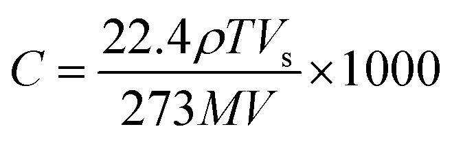 | (1) |
3. Results and discussion
The electrical response of conducting polymer films to alcohol vapors or to humidity is typically quite subdued. Fig. 1a shows a plot of normalized conductance as a function of exposure time to alcohol vapors, and to humidity. A 25% decrease in electrical conductance of the initial value is observed for pristine films exposed to humidity. This decrease of electrical conductance of pristine films exposed to humidity is understood purely from the intrinsic charge transport processes. PEDOT:PSS comprises electrically conducting PEDOT-rich grains that are surrounded by excess insulating PSS layers.26,32,33 At the initial stage of exposure to humidity, PEDOT:PSS thin films swell through the adsorption of water vapor to the superficial layer of the film at a relatively faster rate, and the insulating hydrophilic PSS shell partly loses its hydrophilicity.10,11,15 Subsequently, water vapor diffuses across the film thickness and causes partial reversible swelling of the overall film (Fig. S1 of ESI†). A net increase in the mean separation between conducting PEDOT grains takes place due to water uptake by the hydrophilic PSS shell.10 The percolation pathways for the electronic conduction are slightly disrupted and electrical conductance decreases for the humidity-exposed pristine polymer films. Real time in situ X-ray reflectivity (XRR) measurements are performed on pristine PEDOT:PSS thin film subjected to humidity exposure to obtain the evolution of film thickness as a function of exposure time. A representative plot of PEDOT:PSS film thickness as a function of prolonged exposure time to humidity is shown in Fig. S2 of ESI.† A more extensive study of water-induced swelling of PEDOT:PSS thin films is presented elsewhere.10 The total increase in the film thickness is estimated to be about 29% of the initial value (Fig. S2 of ESI†). The change in electrical response of pristine PEDOT:PSS thin films is even smaller for alcohol vapor exposure. The conductance at saturation response decreases only by about 2%, 5% and 6% for octanol, ethanol and methanol vapor exposure, respectively. We note that the pristine PEDOT:PSS thin film immediately responds to the alcohol vapors and saturates whereas it is a slower process for the humidity exposure. We attribute the smaller change in alcohol vapor response to the limited swelling of the polymer film by the surface adsorption.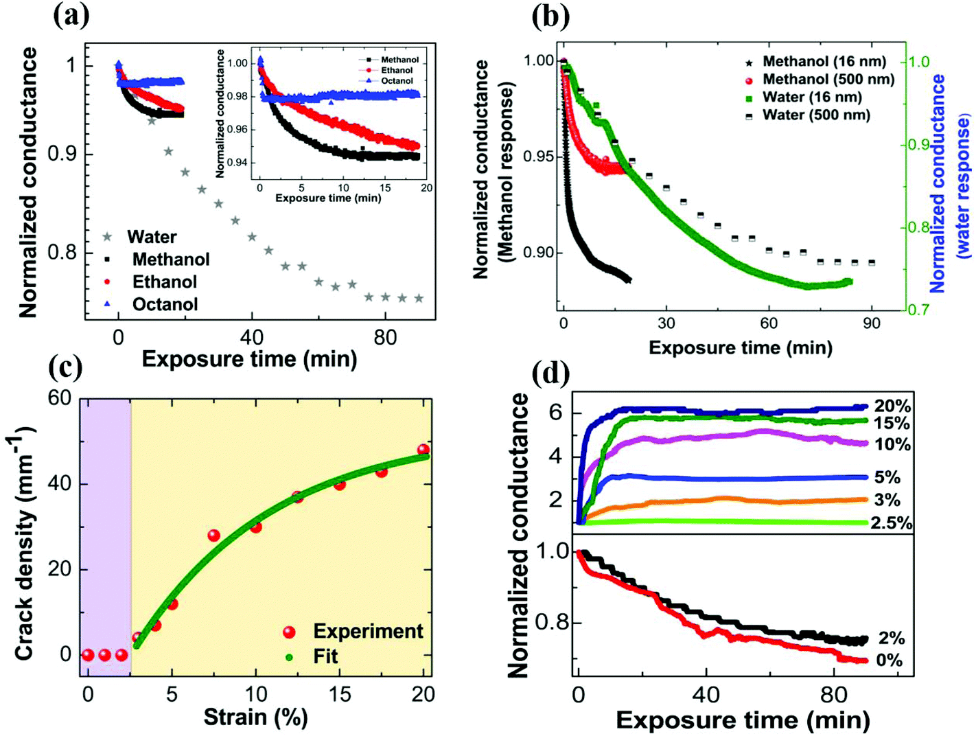 | ||
| Fig. 1 (a) Normalized conductance (G/Gdry) of a pristine PEDOT:PSS thin film (∼500 nm) as a function of exposure time to alcohol vapors (methanol, ethanol and octanol) and to humidity, respectively. The inset shows an enlarged version of the conductance change of the pristine PEDOT:PSS thin film, subjected to alcohol vapors at shorter time scales. (b) Normalized conductance versus exposure time of pristine PEDOT:PSS thin films of varying thickness (16 nm and ∼500 nm) exposed to methanol vapors and humidity, respectively. (c) Plot of crack density as a function of the applied strain. The experimental data are fitted with an empirical formula. (d) Variation of normalized conductance as a function of prolonged exposure time for strained PEDOT:PSS thin films (∼500 nm) exposed to 100% relative humidity (RH). | ||
To further verify this possibility, we have prepared pristine PEDOT:PSS thin films with substantially different film thicknesses and exposed them to methanol vapors as well as humidity. The results are shown in Fig. 1b. Upon water vapor exposure, the normalized conductance change of a thinner PEDOT:PSS film is only slightly more than that for a thicker film. The similar extent of change in normalized conductance for both films of thickness differing by one order (∼30 times) in magnitude indicates that the entire polymer film contributes to the conductance change due to water permeation. The results for methanol are in stark contrast. The PEDOT:PSS film (16 nm) responds much more to the alcohol vapor with ∼12% change in conductance, while the changes are smaller by a factor of 2 for thicker PEDOT:PSS films. The fraction of the film which can be considered to be “in proximity to the surface” is higher for the 16 nm films. Thus, methanol mainly induces conductance changes in the proximity of the surface, while the rapidly diffusing water molecules induce conductance changes in the bulk of the polymer.
Despite the different responses of pristine PEDOT:PSS thin films to water and to alcohol vapors, the general response of the polymer film to any vapor remains feeble and limits its potential applications. To overcome this ordinary response, we consider nanostructuring the polymer films. As a first step towards nanostructuring for enhanced sensing response, the polymer film is subjected to uniaxial strain, which is mathematically defined as ε = [(Lf − Li)/Li] × 100% (in percentage) where ε, Li and Lf are the lengths of the film at zero strain and with the applied strain, respectively. A representative three-dimensional optical profilometry image of the surface morphology of PEDOT:PSS thin film casts on PDMS substrate, after being subjected to uniaxial strain at 20%, is shown in Fig. S3 (ESI†). The extrinsically generated long quasi-periodic parallel cracks appear in a direction perpendicular to the applied strain. The formation of cracks results from the dissipation of strain energy in the thin film.8Fig. 1c clearly shows that a critical strain is required to observe the cracks in the film, which is about 3%. Beyond this strain value, the crack density steadily increases with the applied strain and finally tends towards saturation. The experimental data are fitted with an empirical formula and are given below:26,34
| n(ε) = n0[1 − e−c(ε−ε0)] | (2) |
When the current direction is the same as that of the applied strain, the current pathways are orthogonal to the quasi-periodic cracks. Under these circumstances, the resistance offered by the cracks dominates the total resistance of the polymer films. Thus, for a vapor sensing experiment, the cracked regions alone may dominate the response rather than the bulk film. Next, we evaluate how these strained films (with and without cracks) respond to vapor sensing. Fig. 1d shows a plot of normalized conductance of uniaxially strained PEDOT:PSS thin films as a function of exposure time to saturated humidity (100% RH). The values of strain applied to PEDOT:PSS thin films are varied from 0% to 20%. The thin films of PEDOT:PSS are exposed to humidity for a sufficiently long time (∼90 minutes) to observe the saturation response in conductance, where no further change in electrical conductance upon humidity exposure is realized. Two distinct response regimes can be identified, as shown in Fig. 1d. The conductance of humidity-exposed samples, which are pre-strained between 0% and 2%, shows a decrease in conductance upon humidity exposure. This behavior is similar to the intrinsic response of the film (Fig. 1a). It is noteworthy that 2.5% strain marks the onset value for crack formation. The vapor exposure of cracked films is remarkably different. Firstly, the conductance of all such films (strained to 3% or above) increases upon vapor exposure. Secondly, these changes happen over a much faster time scale when compared to pristine or low strain PEDOT:PSS thin films exposed to humidity. This increase in conduction can be reconciled by considering the swelling of the film near the cracks that mediates the transport by providing further linkages across the cracks, even as the intrinsic (bulk) response leads to reduction in conduction. The 2.5% strained films represent an interesting system where these two counteracting processes are almost evened out so the film is nearly humidity resistant. The crack formation in the conducting polymer is thus a useful knob to manipulate the humidity response of the films. The trend in the data indicates the improved response for films with higher strains. This suggests that further nanostructuring of cracks can enhance the vapor response of the films as measured by the resistance ratio (R/Rdry). The saturation time, which is defined as 10% and 20% decrease of the normalized conductance from the final saturation value, is plotted against the applied strain, and is shown in Fig. S4 (ESI†).
In the previous section, we have seen that strain and cracks can impart tuneability to the humidity response of PEDOT:PSS thin films. Importantly, the conductance of the strained and cracked films increases upon humidity exposure. However, the maximum conductance change is limited to within a factor of six (see Fig. 1d). Now to impart extremely high electrical response of PEDOT:PSS thin films exposed to alcohol vapors or humidity, we first need to understand the morphology of cracks in the stretched PEDOT:PSS thin films. We have discussed in the preceding paragraphs that the application of a uniaxial strain to PEDOT:PSS results in the formation of a quasi-periodic array of cracks. To explore the potential for nanostructuring the cracks that are induced by the uniaxial strain, we considered acquiring micro-Raman spectra of pristine films and 20% strained films with cracks, as shown in Fig. 2a. The characteristic peaks originating at 1258 cm−1, 1371 cm−1 and 1416 cm−1 are assigned to PEDOT and can be attributed to Cα − Cα′, Cβ − Cβ and Cα = Cβ stretching, respectively.35 The Raman intensity for PEDOT:PSS peaks is significantly reduced in the cracked region in 20% strained films. Yet a noticeable amount of PEDOT:PSS is still present in the cracked region. This suggests that strain induced cracks have not completely penetrated the depth of the conducting polymer. Thus, we propose a strategy to nanostructure the crack morphology by removing the residual PEDOT:PSS in the crack region using O2 plasma. This novel and inexpensive crack engineering or nanostructuring process thus comprises straining the films beyond the critical strain value to generate arrays of parallel cracks, followed by controlled exposure to oxygen plasma to alter the crack depth until the crack is nearly open.
 | ||
| Fig. 2 (a) Raman spectra of pristine films and 20% uniaxially strained films with cracks. (b) Conductance as a function of O2 plasma etching time for 16 nm pristine PEDOT:PSS thin film deposited on a glass substrate, and also for a 20% strained PEDOT:PSS thin film on a PDMS substrate, respectively. (c) Cross-section schematic diagram of the film morphology of a uniaxially strained PEDOT:PSS thin film cast on a PDMS substrate. (d) Surface morphology of a 20% strained PEDOT:PSS thin film cast on a PDMS substrate obtained from Scanning Electron Microscopy (SEM) (scale bar: 2 μm). (e) Cross-section schematic diagram showing nanostructured crack morphology of a stretched PEDOT:PSS thin film using O2 plasma etching for a controlled duration. (f) SEM image of the surface morphology of a PEDOT:PSS thin film with nanostructured cracks (scale bar: 2 μm). | ||
The amount of residual PEDOT:PSS in the quasi-periodic cracked regions prior to nanostructuring can also be quantified with electrical measurements. Fig. 2b shows a plot of the conductance of 20% strained PEDOT:PSS on PDMS as a function of O2 plasma etching time. The conductance of the sample is already dominated by the crack regions prior to etching and it further decreases from 8.3 × 10⁻⁶ S to 2 × 10⁻¹¹ S after 300 s O2 plasma etching. Thus, the initial conductance decreases by more than 105 times after the plasma treatment. For comparison, another sample of 16 nm unstrained PEDOT:PSS films is treated with O2 plasma etching under identical conditions. The initial conductance of this film is 9.3 × 10⁻⁴ S and it reaches 5.9 × 10⁻¹¹ S after 200 s O2 plasma etching. Using the latter as a calibration sample and assuming the same etching rate in both experiments, the average thickness of residual PEDOT:PSS in the cracked regions was found to be ∼24 nm. This residual polymer is almost completely removed after 300 s O2 plasma etching, when the film is nearly electrically disconnected. The etching process is arrested, as soon as the film in its cracked region reaches electrical disconnection, defined as G < 5 × 10⁻¹¹ S. While some damage to the un-cracked surface region also happens, the electrical resistance is overwhelmingly dominated by the nano-structured cracks alone. A schematic of the cross-section of the film, which is cracked under strain, is shown in Fig. 2c and a SEM image of the crack is shown in Fig. 2d. It is noteworthy to mention that, not only cracks, quasi-periodic wrinkles that are aligned in a direction parallel to the stretching are also present in a strained film beyond a critical strain value. The evolution of the wrinkle formation is summarized as follows: in general, when a rectangular thin sheet is subjected to the uniaxial applied strain beyond a critical strain value, it exhibits a quasi-periodic wrinkle array in a direction parallel to the stretching direction.36 This strain-induced quasi-periodic wrinkle array can arise from two competing factors: in-plane stretching and out-of-plane bending.36 The formation of a wrinkle array is a robust phenomenon and universal scaling laws for wrinkle wavelength (λ) and amplitude (A) can be evaluated by minimizing the total energy that consists of stretching energy (ES) along the direction of stretching and bending energy (EB) in the direction perpendicular to the stretching.36 In our previous work,26 we have shown that the wrinkle wavelength monotonically decreases as the applied strain increases. Furthermore, we evaluated the applicability of the universal scaling law for the wrinkle wavelength with the applied strain which follows as λ ∼ ε−1/4. We have also tested the universal scaling law for wrinkle amplitude and a non-monotonic dependence of the wrinkle amplitude is found on the applied strain. It can be argued that the scaling laws hold good for crack-free thin sheets under the applied strain. In contrast, our strained film comprises both cracks and wrinkles and the presence of cracks may modify the wrinkle morphology. The modification of the wrinkle morphology could lead to non-monotonic dependence of the wrinkle amplitude on the applied strain.26 The nanostructuring of the crack causes the film in the crack to be nearly removed, as illustrated in Fig. 2e, with a SEM image of the nanostructured crack shown in Fig. 2f. To show the clear morphology of both the crack and the nanostructured crack, a three dimensional atomic force microscopy image has been obtained of the crack and the nanostructured crack, and the images are shown in Fig. S5 (ESI†). Plots of crack depth versus distance along crack width and height fluctuation versus distance along the crack line for cracked films and films with nanostructured cracks are shown in Fig. S5 (ESI†). SEM images of the crack and nanostructured crack morphology on a larger length scale (10 μm for crack and 5 μm for nanostructured crack morphology) are also shown in Fig. S5 (ESI†). The crack width is found to be between ∼1 and 3 μm, depending on the applied strain, prior to etching.
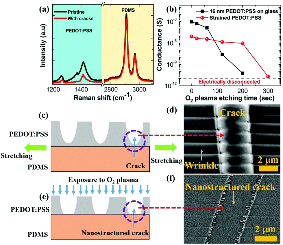
We now discuss the response of these nanostructured PEDOT:PSS thin films when exposed to alcohol vapors of methanol and ethanol. The electrical conductance is recorded as a function of time for varying alcohol vapor concentrations. The concentration of methanol varied from 6 ppm to 300 ppm whereas it is 6 ppm to 327 ppm for ethanol, respectively. A schematic diagram of the experimental setup for alcohol sensing measurements is shown in Fig. S6 (ESI†), and the mathematical formula for the calculation of alcohol concentration is mentioned in the Experimental section.30 The time interval between vapor on and off is about 5 minutes. A plot of conductance as a function of varying concentration of both alcohol vapors is shown in Fig. 3a and b. The sensitivity of the alcohol vapor sensors (S) is defined as S = Rdry/Rswollen, where Rdry and Rswollen are the electrical resistance of the PEDOT:PSS thin film in the absence and presence of alcohol vapor, respectively. The nanostructured PEDOT:PSS thin film exhibits a sensitivity of ∼106 at 300 ppm for methanol and ∼102 at 327 ppm for ethanol, respectively. A representative plot of the sensitivity of the nanostructured PEDOT:PSS thin film as a function of the concentration of the alcohol vapor for both methanol and ethanol is shown in Fig. S7 (ESI†). It is evident that the nominal response of PEDOT:PSS thin films to alcohol vapor (∼6% change for methanol) is enhanced by a massive factor in the nanostructured films, where the resistance changes by many orders of magnitude. This unprecedented response to alcohol vapors for PEDOT:PSS thin films has not been realized previously in the literature.37,38 The response time of the crack-engineered methanol sensor is approximately less than 5 s, which compares favorably with other reports.37,38 Methanol sensors made up of ZnO nanoflowers show a response time, recovery time and sensitivity of 15 s, 100 s and ∼80 times at 400 ppm methanol concentration.39 It is also reported in the literature that the pristine PEDOT:PSS sensor shows a poor response and recovery time of 164 s and 86 s for both methanol and ethanol vapor at 100 ppm alcohol concentration, respectively.37 The sensitivities are shown to be 0.2% and 0.5% for methanol and ethanol vapor, which are extremely poor.37 Also this sensor does not show good selectivity towards any vapors.37 The sensitivity of our nanostructured PEDOT:PSS sensor is not only high but it also shows a selective response to methanol, as compared to ethanol vapor. The steady state response of nanostructured films for methanol and ethanol vapor exposure has also been studied, and representative results are shown in Fig. 3c and d. The on and off times for vapor exposure are kept at 30 minutes. The steady state response for lower concentration of ethanol (6 ppm) is also shown in Fig. S8 (ESI†). For lower concentrations, the conductance of the nanostructured sample reaches the steady state value within 5 minutes.
 | ||
| Fig. 3 (a) Dynamic response of a nanostructured PEDOT:PSS thin film for methanol vapor exposure. (b) Dynamic response of a nanostructured PEDOT:PSS thin film for ethanol vapor exposure. (c) Steady state response for methanol exposure for 65, 140 and 300 ppm. (d) Steady state response for ethanol exposure for 65, 131 and 327 ppm. | ||
We next consider the humidity sensing behavior of nanostructured PEDOT:PSS thin films. The electrical conductance is systematically recorded as a function of time for a humidity-exposed pristine film, a 10% strained film and a nanostructured film, respectively. Firstly, we discuss the dynamic response of electrical conductance upon humidity exposure for a pristine PEDOT:PSS thin film. The origin of the electrical response to the humidity for the pristine PEDOT:PSS thin film has already been discussed and the result is shown in Fig. 1a. The dynamic response of electrical conductance as a function of humidity exposure time for pristine PEDOT:PSS thin film is shown by blue solid squared data points in Fig. 4a. The dynamic switch of RH is maintained between 60% (ambient RH) and 100% for all samples. The time interval for the dynamic switch is 10 minutes for the pristine PEDOT:PSS thin film. Fig. 4a clearly reveals that the variation in the magnitude of the humidity-induced electrical conductance between 60% RH and 100% RH is insignificant, and therefore the sensing behavior of the pristine PEDOT:PSS thin film is very poor and the pristine PEDOT:PSS thin film certainly cannot be used for humidity sensing. Similarly, we have studied the dynamic response of the conductance for a 10% uniaxially strained PEDOT:PSS thin film exposed to humidity, and the response is shown by green triangle data points in Fig. 4a. The overall response of a 10% strained PEDOT:PSS thin film is slightly enhanced compared to the pristine response, but again the sensing response is quite poor. The electrical conductance of a nanostructured PEDOT:PSS thin film as a function of time is also plotted in Fig. 4a; the data points are shown with red spheres. The time interval for the dynamic switch between 60% RH and 100% RH is maintained at 20 minutes. The electrical response is also recorded as a function of prolonged exposure time to 100% RH for the nanostructured PEDOT:PSS thin film, and is shown in Fig. S9 (ESI†). In stark contrast to the previous two samples, the resistance of the nanostructured PEDOT:PSS thin film shows a dramatic response to change in humidity. Again the sensitivity can be defined as S = Rdry/Rswollen, where Rdry and Rswollen are the resistances of the film at 60% RH and 100% RH, respectively. The sensitivity turns out to be 1.5 × 10² with a response time of ∼15 s and a recovery time of ∼16 s. The operating humidity range for our device is 60% to 100% RH. A conductance versus RH (%) plot is shown in Fig. 4b. For comparison with the literature, a humidity sensor comprising a composite of reduced graphene oxide (rGO) and poly(diallyldimethylammonium chloride) (PDAA) shows a relatively poor response time, recovery time and sensitivity of 108 s, 147 s and 1.6 times, although it had a better dynamic range of 11%–97% RH.40 The overall behavior of the conductance measured by varying RH is non-linear in nature. We use a second order polynomial function to describe the dependence of conductance on RH.
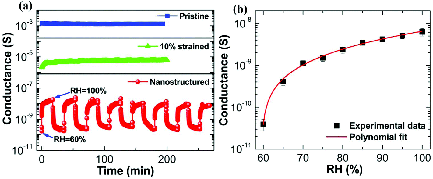 | ||
| Fig. 4 (a) Dynamic response of the conductance of a pristine film, a 10% strained film and a nanostructured PEDOT:PSS thin film exposed to humidity. Conductance at 60% RH and 100% RH is denoted by the lowest conductance and the highest conductance values for a nanostructured PEDOT:PSS thin film, respectively. (b) Conductance versus RH plot for a nanostructured film in the range of 60% to 100%. | ||
The operating range is dependent on the extent of nanostructuring. For the post-etching conductance of 5 × 10⁻¹¹ S, the operating range is 60–100% RH. On the other hand, partially nanostructured samples (lower etching time) show a narrower window of operation along with higher conductance (Fig. S10 of ESI†). Extrapolation of these data sets suggests that the operating range can, in principle, be extended to a wider range by further diminishing the conductance. The long-term stability of our sensor has also been tested on six month and nine month old samples, and the sensing response for the same is shown in Fig. S11 (ESI†). We note that the crack structure remains unaffected after exposure to vapor. As an example, the nanostructured crack morphology before and after exposure to 100% RH is shown in Fig. S12 (ESI†).
We next discuss the possible underlying mechanisms responsible for the vapor-induced large electrical conductance changes for the nanostructured PEDOT:PSS thin films. The conductance change can arise from: (i) enhanced electronic transport in the vapor-exposed nanostructured film, (ii) ionic transport in the vapor condensed in the crack regions. To distinguish these processes, let's consider the origin of an electronically driven process. It is well known that vapors like methanol can induce a coil to linear/extended polymer chain transformation by dissolving excess PSS, thereby enhancing the conduction.41 This opens the possibility that the vapor is inducing such a transformation in the residual polymer in the crack regions, which is reversible upon removal of exposure. To test this scenario, nanostructured PEDOT:PSS samples with protected electrical contacts are immersed in solvents and their resistance is measured, as shown in Fig. 5a. In the immersed state, resistance decreased by several orders of magnitude. The highest response is obtained for immersion in methanol as the solvent, which is consistent with the vapor experiments. However, restoration of the resistance upon removal from the solvents and subsequent drying indicates that the change cannot be attributed to an electronic process like a coil to linear transformation. The latter should induce a permanent change, once excess PSS is dissolved in the solvent. The vapor exposure and liquid immersion experiments induce similar responses on the conduction of nanostructured films, and if these conductance changes have a common origin for both cases, then the electronic process appears unlikely to be the dominant one. Thus, we come to the second possible mechanism, which is the ionic conduction in the presence of the vapor that condenses in the crack regions and forms a meniscus. A meniscus formation has been reported on the surface of vapor-exposed conducting polymer thin films.42 We note that PEDOT:PSS is acidic in nature (pH = 1.6) and H+ ions originating from PSS contribute to the ionic conduction. To further explore this possibility of ionic conduction, we consider the temperature dependence of conductance in the swollen state of nanostructured PEDOT:PSS thin films. For this experiment, the films are hydrated to saturation under 100% RH and cooled to −10 °C in a refrigerator. The results are shown in Fig. 5b. For a detailed description of this experiment see Fig. S13 (ESI†).
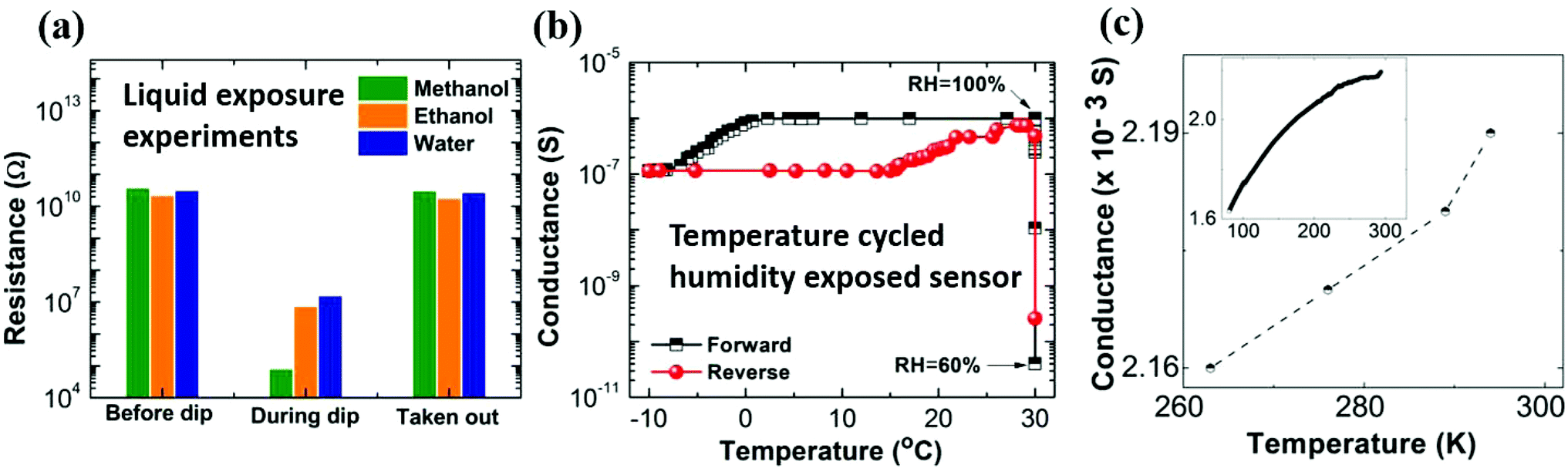 | ||
| Fig. 5 (a) Resistance of a nanostructured PEDOT:PSS thin film measured before and during dipping in methanol, ethanol and water solutions, and also after it was taken out from the solutions. (b) Cyclic response of the conductance of a nanostructured PEDOT:PSS thin film versus temperature in the cycle 30 °C → −10 °C → 30 °C. Black and red data points indicate two distinct temperature cycles (30 °C → −10 °C as a forward cycle and −10 °C → 30 °C as a reverse cycle), respectively. (c) Conductance change as a function of temperature in the range of 263–294 K. The inset shows a conductance versus temperature graph in the interval 80–294 K. The dashed line is a guide to the eye. | ||
The key observation is that the conductance of the swollen film decreases by a factor of ∼9 when the temperature decreases from 30 °C to −10 °C. Such a temperature dependent response is again consistent with ionic conduction. While the ionic composition of the PSS protonated condensed vapor meniscus in the crack is unknown, we can compare our result with typical ionic systems. For example, the resistance ratio for 0.9% saline (R263K/R293K) is 3,43 for pure water (R273K/R300K) it is 4.6.44 We also performed experiments on PEDOT:PSS water dispersion (as received), and PEDOT:PSS in water diluted with water (1:1 v/v ratio) and diluted with methanol (1:1 v/v ratio). In each case, the ionic conduction dropped by a factor of 1.5–3.3 times (Fig. S14 of ESI†). In contrast, the pure electronic conduction of dry state pristine films is nearly constant in this temperature interval (Fig. 5c). The same is also observed for the highly resistive nanostructured PEDOT:PSS thin films, where any changes in conduction in this temperature interval are within the noise level of measurements. Both the solvent immersion and temperature dependent transport experiments strongly suggest the dominance of an ionic conduction process being primarily responsible for the observed conductance changes in vapor-exposed nanostructured films.
A schematic representation of the two contributing transport processes in humidity-exposed nanostructured PEDOT:PSS is shown in Fig. 6. In PEDOT:PSS thin films, typically the charge transport occurs by inter-grain charge transport i.e. hopping of charge carriers between conducting PEDOT grains across intervening PSS layers.10,26,32,33 For nanostructured PEDOT:PSS thin films, the electron percolation path is nearly turned off in a low humidity/vapor concentration due to nearly complete removal of the polymer film inside the cracks by controlled O2 plasma etching, and is shown in Fig. 6a. When this nanostructured PEDOT:PSS thin film is exposed to alcohol vapor or to high humidity, the electron percolation path is partly turned on due to swelling-mediated linkage of the residual polymer in the crack, which then restores the percolation pathway as is shown by the blue region in Fig. 6b. However, the larger contribution arises from the surface ionic conduction from a meniscus of condensed vapor. We may also expect such a mechanism to be at work for large-area PEDOT:PSS films completely etched by O2 plasma. An experiment performed on completely etched 16 nm films revealed alcohol and humidity detection with much subdued values as compared to the nanostructured films (see the table in ESI Table S1†).
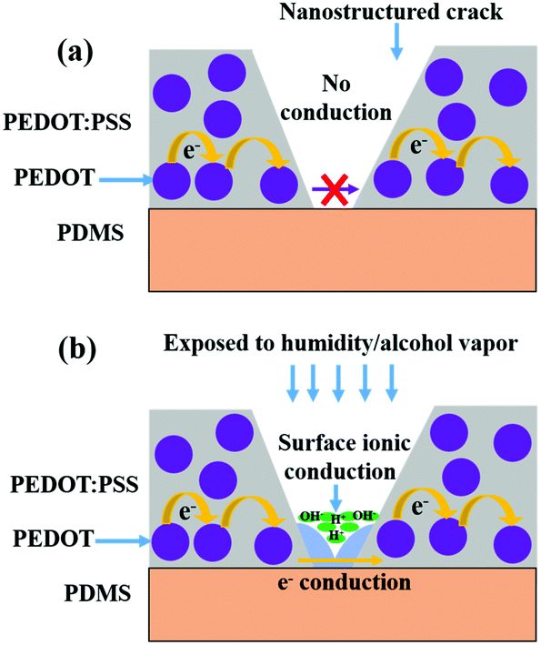 | ||
| Fig. 6 (a) Cross-section schematic diagram of a nanostructured PEDOT:PSS thin film. Conducting PEDOT grains are shown by violet solid circles on either sides of the crack. Electronic conduction between PEDOT grains indicated by the yellow arrow is also shown. (b) Cross-section schematic diagram of nanostructured PEDOT:PSS thin film exposed to high humidity/alcohol vapors. Electronic conduction and surface ionic conduction regions are shown in the schematic. Surface ions in the vapor are shown. The tapering of the crack near the substrate is shown by the blue region. The yellow arrow indicates the electron percolation pathway. | ||
Finally, we showcase the potential of nanostructured PEDOT:PSS thin films for breath analyzer application. Our sensor is ultra-sensitive to detect the alcohol consumed by a human body. Commercially available alcohol (Kingfisher beer with alcohol content ∼6% v/v) is consumed by a volunteer for the sensing test. The pure alcohol mass is calculated from the formula: pure alcohol mass = volume of consumed alcohol (0.375 L) × alcohol by volume (6%) × density of alcohol (789.24 g L−1 at 20 °C). The estimated value of the pure alcohol mass is found to be ∼17.8 g. A breath test is performed beginning ten minutes after the alcohol consumption. The alcohol content is measured using a commercial breath analyzer [model no. A8080P (Medical Sensors, India)] by requiring the volunteer to blow the alcohol-containing breath through a conduit of length 8 cm, diameter 1 cm into the breath analyzer inlet port. An electrochemical sensor that reacts to alcohol was used for detection, and the response was converted using an in-built calibration factor to display the results in Blood Alcohol Content (in mg per 100 ml). In a similar manner, the alcohol-containing breath is blown through a conduit of length 25 cm, diameter 1 cm from a distance of 5 cm above the top surface of our sensor. In the case of the commercial breath analyzer, the sustained flow of breath for a duration of about 5 seconds was verified by an in-built flow sensor, whereas for our device the volunteer was required to blow the breath in an identically sustained manner. The results are displayed in Fig. 7a and b for the commercial breath analyzer and the nanostructured polymer based sensor, respectively. Fig. 7c shows the zoomed in single exposure with alcohol containing breath. The response and recovery times are less than 5 s. The first reading of Blood Alcohol Content (BAC) in the volunteer's body is displayed to be 11 mg per 100 ml by the breath analyzer, and the subsequent conductance change measured by our sensor is unprecedented, which is ∼400 times. While the commercial sensor stops responding after 1.5 hours (noting the very low alcohol content consumed), our sensor continues to show a good response even after 6 hours. The response of the sensor to human breath subsequent to a mouthwash (Listerine cool mint with alcohol content ∼21.6%) gargle is shown in Fig. 7d. Since mouthwash is not absorbed in the blood, the response is obtained for a short duration (∼10 minutes). The data taken with our sensor capture the decay of breath alcohol content with high sensitivity during this short interval. Intervening measurements with normal breath indicate that the sensor is restored to a low conductance state after each exposure. In comparison with the literature, a breath analyzer consisting of an organic electrochemical transistor with PEDOT:PSS printed on paper shows a feeble sensitivity of about 0.15 and 0.18 for breath containing alcohol content 0.06% (wine) and 0.2% (Listerine, 21.6% alcohol content), respectively.17
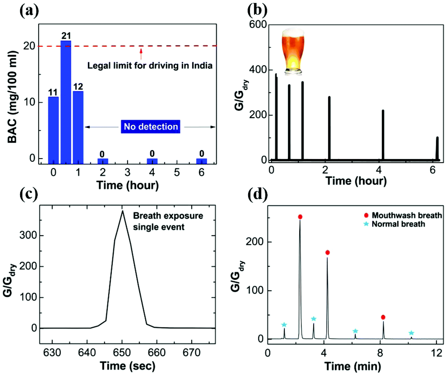 | ||
| Fig. 7 (a) Response of a commercial available breath analyzer (in BAC units) with time, subsequent to alcohol consumption (375 ml beer, alcohol content 6% v/v). (b) Conductance change (G/Gdry) as a function of time for a nanostructured PEDOT:PSS thin film over 6 hours, subsequent to alcohol consumption (375 ml beer, alcohol content 6% v/v). (c) Conductance change (G/Gdry) as a function of time for a nanostructured PEDOT:PSS thin film for a breath exposure single event. (d) Conductance change (G/Gdry) in response to normal breath and to mouthwash breath (alcohol content 21.6%) as a function of time for a nanostructured PEDOT:PSS thin film. | ||
4. Conclusion
Absorption based resistive alcohol vapor and humidity sensors utilizing conducting polymers have been around for quite some time. They are strongly limited in sensitivity and the typical approach has been to look for appropriate composites. In this work, we adopt a novel approach of firstly creating quasi-periodic cracks in a conducting polymer film using strain and the subsequent engineering of crack morphology by controlled plasma etching. These engineered cracks allow the conduction pathways across the cracks to be controllably turned on or turned off in response to alcohol vapor or humidity exposure. A colossal resistance ratio is obtained for nanostructured PEDOT:PSS thin films exposed to the alcohol vapors, in particular, methanol. A strong dependence of electrical conductance is also found on a dynamic switch between ambient humidity and 100% RH. Based on these ideas, we elaborately demonstrate the sensing behavior of nanostructured PEDOT:PSS thin films exposed to alcohol vapor and humidity. The unique idea of nanostructuring is not only useful to design vapor sensors from PEDOT:PSS thin films but also may be applied to other conducting polymers or conducting materials deposited on compliant substrates exhibiting crack formation under mechanical deformation followed by dry etching techniques. Our work establishes a novel route which should open up the opportunities for a new class of vapor sensors based on crack engineered conducting films.Conflicts of interest
IIT Madras has filed an Indian patent (confidential) (patent pending: 201841017186) on the sensor device and the method of preparation described here. This patent and additional patents will be licensed to companies in which none of the authors are employees, officers or directors. All potential conflicts are monitored by regular disclosure to the IIT Madras Office of Industrial Consultancy and Sponsored Projects (IC&SR).Acknowledgements
MJ is thankful to the Department of Science and Technology through DST-SERB grant no. FTP/PS-072/2012 for equipment support. DKS acknowledges funding from the Department of Science and Technology through DST-SERB grant no. EML/2016/003976. We thank Dr Aparna Gupta for help, and the support of CNNP funded by DeitY is also acknowledged.References
- D. Endo, K. Sato and Y. Hayakawa, Phys. Rev. E, 2012, 86, 016106 CrossRef PubMed.
- J. Marthelot, B. Roman, J. Bico, J. Teisseire, D. Dalmas and F. Melo, Phys. Rev. Lett., 2014, 113, 085502 CrossRef PubMed.
- E. Bouchbinder, J. Fineberg and M. Marder, Annu. Rev. Condens. Matter Phys., 2010, 1, 371–395 CrossRef.
- Y. W. Choi, D. Kang, P. V. Pikhitsa, T. Lee, S. M. Kim, G. Lee, D. Tahk and M. Choi, Sci. Rep., 2017, 7, 40116 CrossRef CAS PubMed.
- D. Kang, P. V. Pikhitsa, Y. W. Choi, C. Lee, S. S. Shin, L. Piao, B. Park, K.-Y. Suh, T.-I. Kim and M. Choi, Nature, 2014, 516, 222 CrossRef CAS PubMed.
- S. Chen, Y. Wei, S. Wei, Y. Lin and L. Liu, ACS Appl. Mater. Interfaces, 2016, 8, 25563–25570 CrossRef CAS PubMed.
- Y. Heo, Y. Hwang, H. S. Jung, S.-H. Choa and H. C. Ko, Small, 2017, 13, 1700070 CrossRef PubMed.
- T. Sakorikar, M. K. Kavitha, P. Vayalamkuzhi and M. Jaiswal, Sci. Rep., 2017, 7, 2598 CrossRef PubMed.
- M. Jaiswal and R. Menon, Polym. Int., 2006, 55, 1371–1384 CrossRef CAS.
- B. Sarkar, M. Jaiswal and D. K. Satapathy, J. Phys.: Condens. Matter, 2018, 30, 225101–225110 CrossRef PubMed.
- D. Bailo, A. Generosi, V. R. Albertini, R. Caminiti, R. De Bettignies and B. Paci, Synth. Met., 2012, 162, 808–812 CrossRef CAS.
- E. S. Muckley, C. B. Jacobs, K. Vidal, J. P. Mahalik, R. Kumar, B. G. Sumpter and I. N. Ivanov, ACS Appl. Mater. Interfaces, 2017, 9, 15880–15886 CrossRef CAS PubMed.
- A. Singh and M. Mukherjee, Macromolecules, 2003, 36, 8728–8731 CrossRef CAS.
- T. Samanta and M. Mukherjee, Polymer, 2012, 53, 5393–5403 CrossRef CAS.
- A. M. Nardes, M. Kemerink, M. De Kok, E. Vinken, K. Maturova and R. Janssen, Org. Electron., 2008, 9, 727–734 CrossRef CAS.
- Z. Kennedy, J. Christ, K. Evans, B. Arey, L. Sweet, M. Warner, R. Erikson and C. Barrett, Nanoscale, 2017, 9, 5458–5466 RSC.
- E. Bihar, Y. Deng, T. Miyake, M. Saadaoui, G. G. Malliaras and M. Rolandi, Sci. Rep., 2016, 6, 27582 CrossRef CAS PubMed.
- S. R. Dupont, F. Novoa, E. Voroshazi and R. H. Dauskardt, Adv. Funct. Mater., 2014, 24, 1325–1332 CrossRef CAS.
- C. Duc, G. G. Malliaras, V. Senez and A. Vlandas, Synth. Metal., 2018, 238, 14–21 CrossRef CAS.
- F. Greco, A. Zucca, S. Taccola, A. Menciassi, T. Fujie, H. Haniuda, S. Takeoka, P. Dario and V. Mattoli, Soft Matter, 2011, 7, 10642–10650 RSC.
- J. Kim, J. Jung, D. Lee and J. Joo, Synth. Met., 2002, 126, 311–316 CrossRef CAS.
- J. Ouyang, Q. Xu, C.-W. Chu, Y. Yang, G. Li and J. Shinar, Polymer, 2004, 45, 8443–8450 CrossRef CAS.
- S. Lai, M. Chan, M. Fung, C. Lee and S. Lee, Mater. Sci. Eng., B, 2003, 104, 26–30 CrossRef.
- Q. Wei, M. Mukaida, Y. Naitoh and T. Ishida, Adv. Mater., 2013, 25, 2831–2836 CrossRef CAS PubMed.
- Y. Kim, A. M. Ballantyne, J. Nelson and D. D. Bradley, Org. Electron., 2009, 10, 205–209 CrossRef CAS.
- B. Sarkar, D. K. Satapathy and M. Jaiswal, Soft Matter, 2017, 13, 5437–5444 RSC.
- B. Sarkar, D. K. Satapathy and M. Jaiswal, AIP Conf. Proc., 2018, p. 110036.
- B. Charlot, G. Sassine, A. Garraud, B. Sorli, A. Giani and P. Combette, Microsyst. Technol., 2013, 19, 895–903 CrossRef CAS.
- M. ElMahmoudy, A. M. Charrier, G. G. Malliaras and S. Sanaur, Adv. Mater. Technol., 2018, 3, 1700344 CrossRef.
- D. Zhang, J. Liu, H. Chang, A. Liu and B. Xia, RSC Adv., 2015, 5, 18666–18672 RSC.
- G. Kunte, U. Ail, S. Shivashankar and A. Umarji, Bull. Mater. Sci., 2005, 28, 243–248 CrossRef CAS.
- C. S. Sangeeth, M. Jaiswal and R. Menon, J. Appl. Phys., 2009, 105, 063713 CrossRef.
- C. S. Sangeeth, M. Jaiswal and R. Menon, J. Phys.: Condens. Matter, 2009, 21, 072101 CrossRef PubMed.
- S.-H. Jen, J. A. Bertrand and S. M. George, J. Appl. Phys., 2011, 109, 084305 CrossRef.
- S. H. Chang, C.-H. Chiang, F.-S. Kao, C.-L. Tien and C.-G. Wu, IEEE Photonics J., 2014, 6, 1–7 Search PubMed.
- E. Sharon, B. Roman, M. Marder, G.-S. Shin and H. L. Swinney, Nature, 2002, 419, 579 CrossRef CAS PubMed.
- J. N. Gavgani, H. S. Dehsari, A. Hasani, M. Mahyari, E. K. Shalamzari, A. Salehi and F. A. Taromi, RSC Adv., 2015, 5, 57559–57567 RSC.
- M. A. Dos Reis, F. Thomazi, J. Del Nero and L. S. Roman, Sensors, 2010, 10, 2812–2820 CrossRef CAS PubMed.
- D. Acharyya, N. Banerjee and P. Bhattacharyya, Sensors, 2014 IEEE, 2014, pp. 811–814.
- D. Zhang, J. Tong and B. Xia, Sens. Actuators, B, 2014, 197, 66–72 CrossRef CAS.
- D. Alemu, H.-Y. Wei, K.-C. Ho and C.-W. Chu, Energy Environ. Sci., 2012, 5, 9662–9671 RSC.
- M. Kuş and S. Okur, Sens. Actuators, B, 2009, 143, 177–181 CrossRef.
- R. Sauerheber and B. Heinz, Chem. Sci. J., 2015, 6, 1 Search PubMed.
- T. S. Light, Anal. Chem., 1984, 56, 1138–1142 CrossRef CAS.
Footnote |
| † Electronic supplementary information (ESI) available. See DOI: 10.1039/C8NR07230B |
| This journal is © The Royal Society of Chemistry 2019 |