
Localization and transient emission properties in InGaN/GaN quantum wells of different polarities within core–shell nanorods
Y.
Robin
 ab,
E. A.
Evropeitsev
c,
T. V.
Shubina
*c,
D. A.
Kirilenko
c,
V. Yu.
Davydov
c,
A. N.
Smirnov
c,
A. A.
Toropov
c,
I. A.
Eliseyev
c,
S. Y.
Bae
ad,
M.
Kushimoto
e,
S.
Nitta
a,
S. V.
Ivanov
c and
H.
Amano
ab
ab,
E. A.
Evropeitsev
c,
T. V.
Shubina
*c,
D. A.
Kirilenko
c,
V. Yu.
Davydov
c,
A. N.
Smirnov
c,
A. A.
Toropov
c,
I. A.
Eliseyev
c,
S. Y.
Bae
ad,
M.
Kushimoto
e,
S.
Nitta
a,
S. V.
Ivanov
c and
H.
Amano
ab
aInstitute of Materials and Systems for Sustainability (IMaSS), Nagoya University, Japan. E-mail: yoann.robin@imass.nagoya-u.ac.jp
bCenter for Integrated Research of Future Electronics (CIRFE), Nagoya University, Japan
cIoffe Institute, 194021 St. Petersburg, Russia. E-mail: shubina@beam.ioffe.ru
dKorea Institute of Ceramic Engineering and Technology, Jinju, South Korea
eDepartment of Electrical Engineering and Computer Science, Nagoya University, Japan
First published on 15th November 2018
Abstract
Transient photoluminescence (PL) characteristics and localization phenomena in InGaN/GaN core–shell nanorods (NRs) were investigated from 6 K up to 285 K. The NRs exhibit three well-defined PL bands in the near-UV, blue, and green range ascribed to the emission of quantum well (QW) areas situated at the (1.00) sidewalls, (10.1) top facets, and (00.1) tip, respectively. At low temperature, time-resolved PL shows a fast decay time of about 0.5 ns for the semi- and non-polar QWs, while the polar QWs exhibit at least a twice-longer time. Rapid delocalization of carriers above 50 K indicates shallow potential fluctuations in the QWs. At room temperature, the characteristic fast PL decay time of the three QW bands stabilizes around 300 ps. The slow decaying PL components have different characteristic decay times that are explained by additional localization at basal stacking faults (BSFs), taking into account the quantum confined Stark effect. In addition, narrow excitonic luminescence lines are observed in the BSF-enriched polar QWs, providing direct evidence of the impact of the BSF/QW crossings on the optical properties of the NRs. A PL rise time of about 100 ps does not show any deviation between bands. These findings are suggestive of similar transport mechanisms in temperature equilibrium without inter-facet transport between different QWs. We believe that predictable transient characteristics can play a key role in creating uniform NR ensembles for device applications.
Introduction
III-Nitride nanorods (NRs) are exciting nanoscale objects of high crystal quality and extended surface planes which have different polarities. Due to their small size and low footprint, they can be grown on substrates with high lattice or thermal mismatch.1 During the earliest stage of the growth, the misfit dislocations generated at the interface can bend toward the sidewalls of the NRs, leading to crystals with few or no extending defects.2,3 The NRs have numerous promising applications. Their extremely small dimensions are expected to allow the fabrication of efficient core–shell micro-LED displays with extra high resolution. In addition, the modification of the growth kinetics of the quantum wells (QWs) on different polar, semi-polar, and non-polar facets enables the simultaneous emission of different colors by a single NR. Such a characteristic could be useful for the design of multi-wavelength devices.4–6However, the InGaN/GaN core–shell QWs suffer from a lack of homogeneity induced by the specifics of the growth kinetics.7 This results in an indium rich pseudo-quantum dot (QD) at the tip and QW thickness variations along the sidewalls of the rods.8 Transmission electron microscopy (TEM) studies demonstrated the QW thickness and composition gradients along the facets.2,5,9,10 A high density of basal stacking faults (BSFs) is typical of the NR tips and sidewalls.5 At the intersection of the BSF with a QW, the energy lowering due to the discontinuity of the polarization at the BSF interfaces can be as high as 60–100 meV.11,12 However, the data on the influence of the BSFs on the optical properties of the NRs and nanocolumns are controversial: both enhanced recombination of carriers12 and emission quenching13 at the NRs were confirmed by micro-spectroscopy studies. The realization of NR-based devices requires a full understanding of the fundamental characteristics of such structures and the elucidation of these controversial issues. Therefore, various studies aim at investigating the spatial distribution of the indium composition and dopant concentration on the overall surface, with particular attention to the apex sub-structure and the facet junctions.14,15 To that purpose, analyses with high spatial resolution were often performed including techniques such as depth-resolved photoluminescence (PL),16 atomic probe tomography (APT),17 nano-cathodoluminescence (nano-CL)10,14,15,18 and TEM.3,5,8
Time-resolved photoluminescence (TRPL) is a powerful spectroscopic technique that can provide important information on the dynamics of the carriers inside the structure. However, in the case of NRs, the complexity of the signals coming from the facets of different polarities makes the analysis challenging. Indeed, conventional planar InGaN/GaN QWs already present TRPL signals with two main exponential decays – fast and slow components that indicate different possible recombination scenarios which are still under study. First, it was suggested the dominant processes could be related to the recombination of carriers in extended and localized states within the QWs.19,20 More recently, it was proposed that the thickness and compositional fluctuations, i.e. the potential profile fluctuation within QWs, could be responsible for these.21 For the analysis of the TRPL data, the model suggested by Iwata et al.,22 which is based on the rate equations accounting for the radiative and non-radiative channels, appears very suitable. In particular, its application enabled the discovery of the impact of the non-radiative Auger process on the fast recombination.23 Thus, NR based core–shell structures presenting three types of QWs of different polarities obviously display a complex TRPL signal that results from the superposition of several recombination channels. More generally, the radiative and non-radiative pathways strongly depend on the QW quality and on the defects associated with each facet polarity.
In this study, we focus on the transient PL of QWs deposited on the NRs, displaying well-separated emission bands of non-polar, semi-polar and polar QWs. We discuss the general issues of carrier localization and inter-facet transport within these core–shell structures based on the evolution of the fast and slow decay times with temperature, as well as the intensity of each component. In order to specify the impact of the BSFs, we measured the micro-PL in NRs that enables us to observe the narrow emission lines related to the intersections of the BSF with the polar QWs at the NR tips.
Experiments and discussion
By means of nanoimprint lithography and dry etching processes, holes of 490 nm diameter with a pitch of 1360 nm were opened in a 30 nm thin SiO2 layer deposited on a Si-doped GaN template grown on silicon. Then, the sample was introduced into an EpiQuest showerhead metal–organic vapor phase epitaxy (MOVPE) reactor and NRs with a diameter and length of 0.8 and 1.5 μm, respectively, were grown by pulsed selective area epitaxy. Then, the rods were covered by a set of five InGaN/GaN QWs followed by a 50 nm p-GaN layer. The growth conditions are similar to those in ref. 5. The InGaN/GaN core–shell NRs were studied by macro-PL and micro-PL spectroscopy at different temperatures. For the macro-PL measurement, we used a 4th harmonic (λ = 210 nm) of a Ti:sapphire femtosecond pulsed laser operating at a frequency of 76 MHz. The laser spot size and average power were estimated to be about 400 μm in diameter and 300 μW, respectively. The pulse duration was 150 fs. The PL emission was dispersed by a spectrometer and, then, its decay curves were detected using a time-correlated single photon counting technique with a temporal resolution equal to or less than 145 ps. For the micro-PL, the laser (λ = 442 nm) spot size was about 2 μm in diameter and the excitation power was 100 μW. TEM studies were performed by using a Jeol JEM-2100F microscope with an accelerating voltage of 200 kV and a point-to-point resolution of 0.19 nm. Conventional bright-field, dark-field and electron diffraction imaging were used to analyze the defects and phase structures of the NRs.Fig. 1 presents the multi-band photoluminescence (PL) of the nanorods recorded at 6 K and 285 K, referred to as low temperature (LT) and room temperature (RT), respectively. At LT, the peak centered at 359 nm corresponds to the band-edge (BE) emission of GaN. The narrow full width at half maximum (FWHM) of about 2 nm and the bandgap narrowing of about 6 nm observed from LT to RT are typical of a material of high quality.24,25 Since GaN constitutes the core of the NR structures, we expect the QW shell to exhibit such crystal quality. The peak at 389–393 nm is related to the non-polar (1.00) sidewalls. It exhibits an intensity decrease by 15 from LT to RT and the small wavelength shift (about 4 nm) roughly follows the evolution of the BE signal. The FWHM of 16 nm attests to the good general quality of this QW emission.26 The blue band peaking at 429–454 nm is slightly broader and its PL intensity decreases by 11 from LT to RT. The large wavelength shift with temperature (about 25 nm) suggests the presence of carrier localization enhanced by strong QW fluctuations. By means of TEM and various optical characterization processes, we previously ascribed this band to the non-uniform semi-polar (10.1) QWs whose nominal thickness deviates along the top facets.5
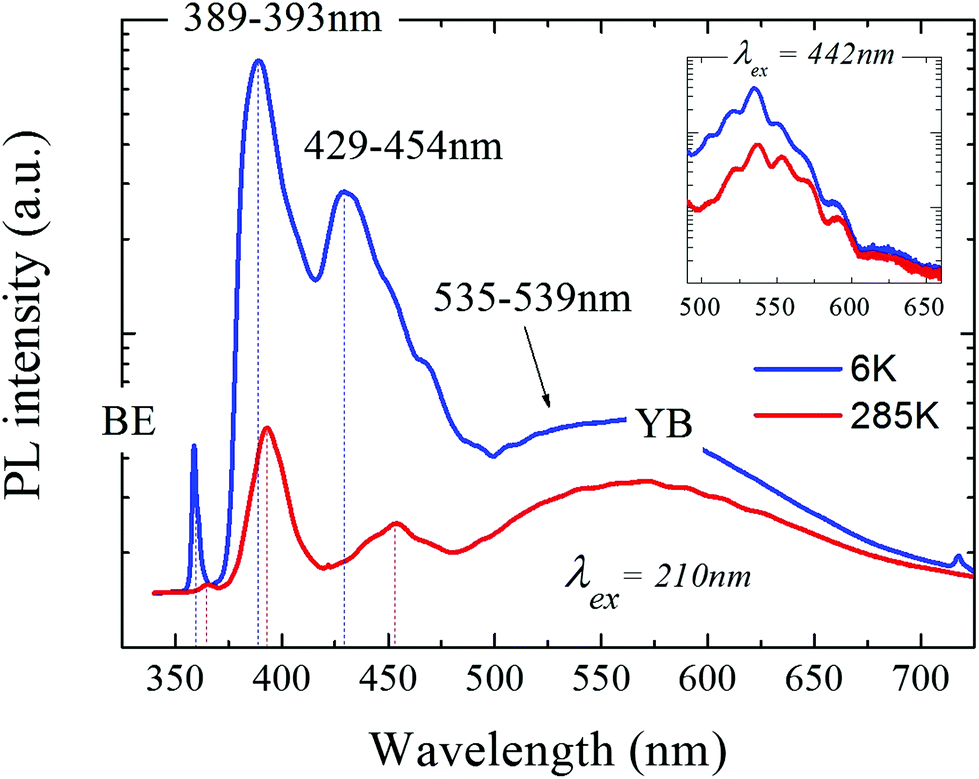 | ||
| Fig. 1 Multi-band macro-PL spectra of the NRs at 6 K and 285 K. The inset shows the micro-PL spectra with a significantly reduced YB, which allows a better separation of the green contribution. Note the different excitation wavelengths of the micro-PL, which was recorded from the top of a NR. | ||
The typical yellow-band (YB) originating from the deep defects of the GaN is also observed at a longer wavelength. We suggest that this luminescence mainly arises from the polycrystalline (In)GaN deposited on the SiO2 mask. Indeed, using a micro-PL system with a spot size of about the typical rod diameter, we could significantly reduce the YB intensity. At the same time, the resonant excitation enhances an additional PL band centered around 535 nm at LT, which is modulated by strong Fabry–Perot oscillations (Fig. 1 (inset)). This band, ascribed to the polar QWs of the NR tip, was masked by the YB signal with the higher-energy excitation above the GaN edge. It should be noted that the 442 nm excitation is not suitable to excite the luminescence of the deep defects in the GaN core, which is mostly fed on by photo-carriers created by excitation above the GaN absorption edge. However, the contribution of the deep defects in the GaN core cannot be excluded as it was confirmed by our measurements of NRs without any shell, as well as by the results reported by Muller et al.10 Thus, both contributions of defects inside and outside the GaN core are responsible for the yellow emission. Finally, we would like to highlight that the ascription of the three emission bands to the (10.0), (10.1) and (00.1) QWs was further confirmed by both PL and electroluminescence (EL) measurements showing respective negligible, moderate and strong QCSE screening at higher excitation power and injection current.5
In order to estimate the characteristic time of the different QW emissions, TRPL measurements were first carried out at LT. Fig. 2 presents the fast decay time measured at different wavelengths along the PL contour and the inset illustrates the transient PL signals recorded for the three QW contributions at 389, 430 and 538 nm. It should be noted each TRPL signal could be fitted by a bi-exponential decay function except the blue band, whose fitting was not ideal at 6 K. More generally, the accuracy of the fitting was better at higher temperature, indicating the presence of additional localization mechanisms at LT. The fast characteristic time τ1 of about 0.5 ns recorded for the near-UV and blue peaks at LT is typical of non-polar and semi-polar QWs.27 Indeed, the smaller QCSE present on these surfaces leads to a better wave-function overlap, i.e. an enhanced radiative recombination rate. Although the value of the fast decay time measured at 538 nm (τ1 ∼ 1–2 ns) is lower than previously reported results,23 it is rather consistent with polar QWs that are prone to a larger QCSE, stronger carrier localization, and weaker electron–hole coupling.28 However, the TRPL decay curves in the inset of Fig. 2 point out a slower decay time τ2, likely associated with deeper defects.
 | ||
| Fig. 2 Spectrum and fast decay time τ1 of the PL comprising bands at different wavelengths. The inset illustrates the TRPL signals (blue) and their bi-exponential fits (red) at the three main contributions indicated by the black arrows. For visibility, decay curves measured at 430 nm and 538 nm are multiplied by 1.5 and 20, respectively. | ||
Fig. 3(a) shows the evolution of the fast decay time from LT to RT. The TRPL performed at 359 nm (squares and solid line) is typical of the GaN band edge emission. The fast decay time rapidly decreases at low temperatures indicating a very small exciton localization energy.29 The near UV (circles and dotted line) and blue (triangles and dashed line) bands show somewhat deeper carrier localization with a characteristic time τ1 of about 525 and 575 ps, respectively, at 6 K. The temperature quenching starts at 50 K, indicating a rather shallow localization energy of several meV, and then τ1 rapidly decreases to reach the same level as GaN. As previously suggested by Lin et al.,21 such shallow localization could originate from QW thickness fluctuations. The composition variation cannot be excluded as well. We observed by TEM a variation of about 20–25% of the QW thickness between the top and the bottom of both sidewalls and top facets.5 Such gradual variation contributes to the enhancement of the spectral bandwidth, while the nano-scale variations in both thickness and composition can act as shallow localization sites. The carriers easily escape from there with the temperature rise. A longer characteristic time τ1 with a higher degree of localization is observed for the green band, consistent with a larger QCSE associated with polar QWs.30
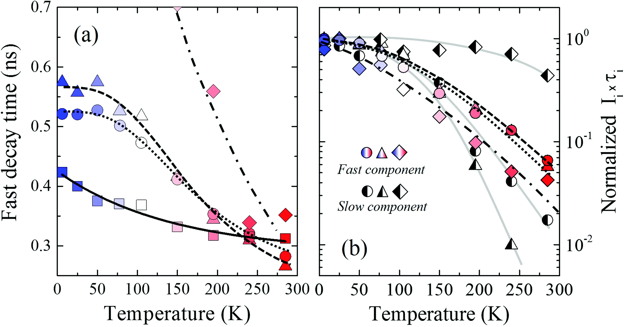 | ||
| Fig. 3 (a) Temperature dependence of the fast decay time of the 359–365 nm (square, solid line), 389–393 nm (circle, dot line), 429–454 nm (triangle, dashed line) and 535–539 nm (diamond, dash-dot line) bands. (b) Temperature dependence of the normalized integral intensity of the decaying PL bands. | ||
Fig. 3(b) illustrates the normalized integral intensity of both slow and fast components of the PL of each QW band. While the intensities of the fast components decrease similarly with the temperature, the difference between the slow components is more pronounced. In particular, the near-UV and blue bands are rather similar at LT but their localization is slightly deeper in the non-polar sidewalls. The slow decaying component is surprisingly enhanced in the m-QWs in spite of their relative uniformity compared with the semi-polar QWs, which are more inhomogeneous in thickness and have more than two PL components at LT and a broad feature at RT (see Fig. 1). The c-QWs clearly show a slower decaying component with a characteristic time of a few tens of nanoseconds, which is attributed to the carrier separation at the opposite interfaces by built-in electric fields in the thick polar QWs, controlled by the QCSE. However, as discussed above, its fast time of about 1–2 ns is rather low for polar QWs.23 Such features impel us to consider the impact of BSFs on the transient properties.
We have systematically observed the BSFs in the TEM images of the NRs (Fig. 4). They can cross any place of the non-polar and semi-polar QWs and penetrate through the polar QWs. The BSF performance should depend on which type of QW is intersected. To clarify this, let us consider two limiting cases: (1) non-polar QWs and (2) polar QWs (the semipolar QWs are somewhere between them). The non-polar QWs without BSFs do not suffer from the QCSE, but when the BSFs cross these QWs, the discontinuity appears along the c-axis at the 1D-like QW/BSF intersections.11 Therefore, the excitons experience different types of confinement in two orthogonal directions (see the band diagram illustrations in Fig. 4(a)). Such a situation could explain the long slow-decaying component in this emission band of the non-polar QWs (τ2 ≥ 30 ns).11,31 In contrast, when the BSFs penetrate the polar QWs undergoing the QCSE,32 the discontinuity at the BSFs is affected by the carrier charges accumulated at the QW interfaces. They push both the electron and hole wave functions of the exciton bound at the BSFs toward each other, resulting in an increased overlap of electron–hole wave functions, i.e. in a faster recombination rate. Such a situation resembles the staggered InGaN QWs, which demonstrates enhanced emission from a central QW (see the band diagram illustration of Fig. 4(b)).33 Interestingly, the BSF/QW crossings are perfect atomically thin planes of BSFs which can provide additional narrow excitonic lines that can be observed up to room temperature.34 Therefore, we expect the polar QWs to have an admixture of emissions originating from the BSF/c-QW intersections. In addition, these emissions should be less redshifted than the defect-free c-QW emission which is prone to the strong QCSE. It should be noted that it is opposite to the case of BSF/m-QW crossings, whose recombination energy commonly exhibits a lowering of the order of 0.1 eV.12
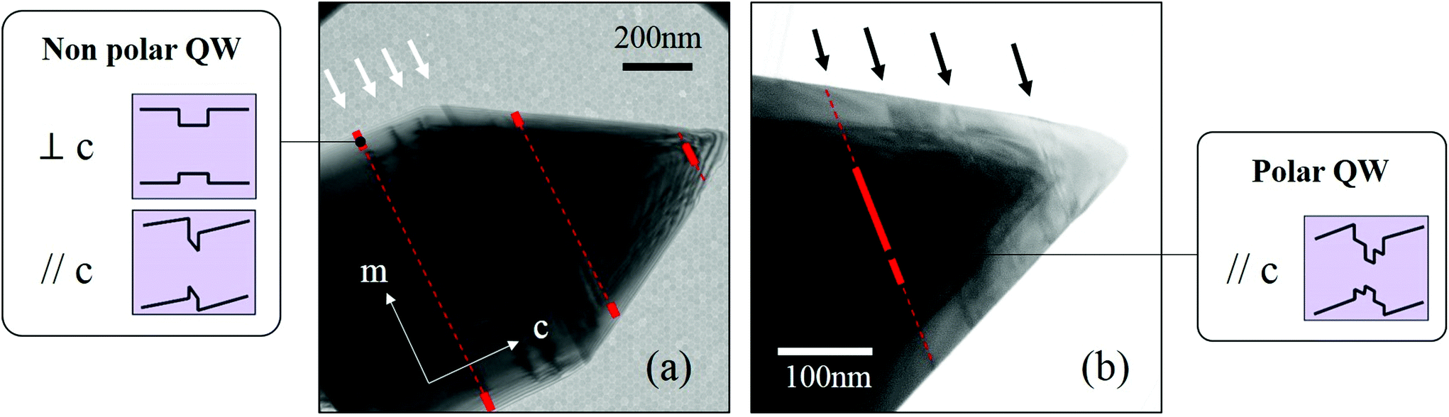 | ||
| Fig. 4 TEM images of NRs showing stacking faults, represented by the black and white arrows, crossing the sidewall (a) and located at the tip (b). Band diagram illustration of the polar and non-polar QWs crossing the BSFs parallel and perpendicular to the c direction. | ||
To prove this assumption, we performed μ-PL measurements on individual NRs to record such narrow spectral features. Fortunately, they were registered in the anticipated green spectral range (Fig. 5). The weak PL emission from the BSF-free polar QWs, whose intensity is reduced by the QCSE, enabled the observation of narrow lines of the excitons bound at the BSF/polar-QW intersection. For this experiment, we removed several NRs from the substrate and measured the PL spectra at different points along the NRs. The narrow lines appear when the laser spot approaches the NR tip. The following TEM studies of the same NRs confirm the presence of the BSFs. Importantly, in the NRs where the polar QWs were not (properly) formed at the tip, we failed to find such narrow lines in the top region. Such lines were also absent in the NRs free of BSFs. Thus, only polar QWs nesting the BSFs can provide such extra-strong excitonic lines. The observation of the narrow excitonic lines proves the strong impact of the BSF on the optical properties of the NRs. It can explain the peculiarities such as the longer decay time of the PL from the more uniform sidewall QWs as compared with the inhomogeneous semi-polar QWs, because the discontinuity of the band structure along the c-axis at the BSFs is higher. The pronounced fast PL contribution from the polar QWs can partly be due to the faster recombination at the BSF/c-QW intersections (although we cannot exclude the recombination at the non-radiative centers in these too thick wells as well).
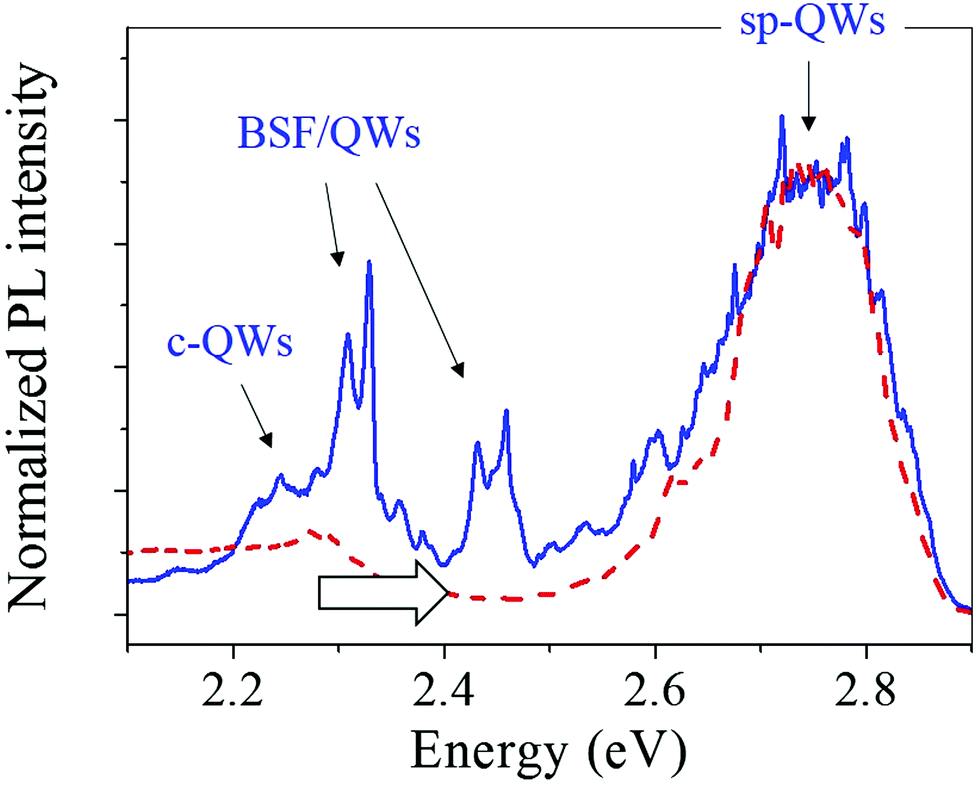 | ||
| Fig. 5 Micro-PL spectra measured at the tips of NRs, with (solid blue line) and without (dashed red line) the polar QWs enriched by BSFs. Note that the onset of the emission from the polar QWs is red-shifted due to the QCSE (white arrow). | ||
At RT, balanced delocalization, transport and radiation processes with characteristic times of about 300 ps are similar in both QWs and GaN as depicted in Fig. 3(a). Thus, one can assume similar transport characteristics of carriers in all these regions. However, to investigate the potential inter-facet transport, we analyzed the rise time of the PL signal, which gives the information on the arriving time of the photo-generated carriers. When the inter-facet transport exists, we expect a carrier transfer from higher energetic levels toward lower ones, further leading to a delay of the rise time. For instance, Oto et al. found a 130 ps difference in the rise of well-defined PL bands attributed to the carrier transport between closely situated QW regions at the top of NRs.35 In our case, we would expect a similar carrier transfer from near-UV and blue QWs toward blue and green QWs, respectively. Fig. 6 compares the rise time of the TRPL signals of GaN and the three QW contributions at LT and RT. The rise time of the GaN band-edge emission is independent of the temperature, as it takes about 75 ps for the signal to reach its maximum at both LT and RT. However, all the QW bands appear with a similar delay of about 100 ps and 85 ps at LT and RT, respectively. Therefore, we concluded that there is no evidence of inter-facet transport between the wells in our NRs. This is supported by the facet dimension of the NRs of about 1 μm, which is significantly larger than the carrier diffusion length in InGaN (∼100 nm).36 The difference in dimensions is likely the reason for our difference from the previous studies involving the carrier transfer.35
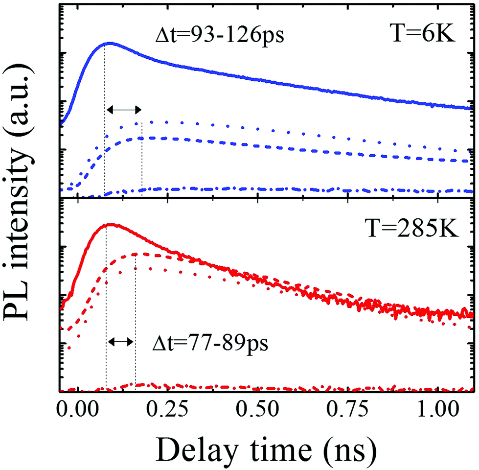 | ||
| Fig. 6 TRPL of the 359–365 nm (solid line), 389–393 nm (dot line), 429–454 nm (dashed line) and 535–539 nm (dash-dot line) bands recorded at 6 K and 285 K. Note that the intensity of the PL is not zero at t = 0 ns because the slow component of the decaying bi-exponential signals is comparable with the period between laser pulses. | ||
Conclusion
We investigated the carrier dynamics of multi-color InGaN/GaN NRs by means of integrated and time-resolved PL. Well-separated emissions allowed us to independently study the fast and slow components of the decaying signal coming from the polar, semi-polar and non-polar facets. The fast characteristic time of the TRPL of QWs on the sidewalls and top facets demonstrated a shallow localization partly related to thickness fluctuations observed by means of TEM. The slow decaying component was attributed to deeper localized states, presumably BSFs. Different densities and characters of BSF/QW intersections on various NR facets can explain the observed difference in the slow decay time values. The thick polar QWs at the tip of NRs, enriched by the BSFs, exhibited a long PL decay tail due to the inherent Stark effect, while the recombination at the penetrating BSF planes can be markedly faster. In addition, narrow excitonic luminescence lines were recorded in the BSF-enriched polar QWs, providing direct evidence of the impact of the BSF/QW crossings on the optical properties of the NRs. While the localization and transport were different for each band at LT, similar characteristic fast decay times were observed at RT, suggesting similar balanced delocalization, transport and radiation near equilibrium. Although the transport towards the thicker regions within the same QW on non-polar, semi-polar and polar planes is still under question, we did not find any evidence of inter-facet transport. Thus, spectral separation of different QW regions could simplify designing multi-wavelength devices exploiting such core–shell NRs.Author contributions
Y. R. and S. Y. B. grew the materials, and Y. R. wrote the manuscript with the assistance of E. A. E. and T. V. S. The STEM and (TR)PL measurements were performed by D. A. K., E. A. E., V. Yu. D., I. A. E., A. N. S., and A. A. T. V. N. J., M. K. and S. N. contributed to the data analysis. S. V. I. and H. A. supervised the project. All authors discussed the results and reviewed the manuscript.Conflicts of interest
There are no conflicts to declare.Acknowledgements
The work at IMaSS is supported by the Japan Society for the Promotion of Science “Bilateral Exchange Project-Collaboration with Russia RFBR and with France CNRS”. The optical characterization at the Ioffe Institute is supported by the Russian Science Foundation (project #14-22-00107). The STEM measurements were performed using equipment of the Federal Joint Research Center “Material science and characterization in advanced technology” (project MES RF #RFMEFI62117X0018).References
- A. Waag, X. Wang, S. Fündling, J. Ledig, M. Erenburg, R. Neumann, M. Al Suleiman, S. Merzsch, J. Wei, S. Li, H. H. Wehmann, W. Bergbauer, M. Straßburg, A. Trampert, U. Jahn and H. Riechert, Phys. Status Solidi C, 2011, 8, 2296–2301 CrossRef CAS.
- M. Mandl, X. Wang, T. Schimpke, C. Kölper, M. Binder, J. Ledig, A. Waag, X. Kong, A. Trampert, F. Bertram, J. Christen, F. Barbagini, E. Calleja and M. Straßburg, Phys. Status Solidi RRL, 2013, 10, 800–814 CrossRef.
- S.-Y. Bae, B. O. Jung, K. Lekhal, S. Y. Kim, J. Y. Lee, D.-S. Lee, M. Deki, Y. Honda and H. Amano, CrystEngComm, 2016, 18, 1505–1514 RSC.
- Y. J. Hong, C. H. Lee, A. Yoon, M. Kim, H. K. Seong, H. J. Chung, C. Sone, Y. J. Park and G. C. Yi, Adv. Mater., 2011, 23, 3284–3328 CrossRef CAS PubMed.
- Y. Robin, S. Y. Bae, T. V. Shubina, M. Pristovsek, E. A. Evropeitsev, D. A. Kirilenko, V. Yu. Davydov, A. N. Smirnov, A. A. Toropov, V. N. Jmerik, M. Kushimoto, S. Nitta, S. V. Ivanov and H. Amano, Sci. Rep., 2018, 8, 7311 CrossRef CAS PubMed.
- Y. Robin, Y. Liao, M. Pristovsek and H. Amano, Phys. Status Solidi A, 2018, 215, 1800361 CrossRef.
- Y. Kangawa, T. Akiyama, T. Ito, K. Shiraishi and T. Nakayama, Materials, 2013, 6, 3309–3360 CrossRef CAS PubMed.
- B. O. Jung, S.-Y. Bae, S. Lee, S. Y. Kim, J. Y. Lee, Y. Honda and H. Amano, Nanoscale Res. Lett., 2016, 11, 215–210 CrossRef PubMed.
- E. D. Le Boulbar, P. R. Edwards, S. H. Vajargah, I. Griffiths, I. Gîrgel, P.-M. Coulon, D. Cherns, R. W. Martin, C. J. Humphreys, C. R. Bowen, D. W. E. Allsopp and P. A. Shields, Cryst. Growth Des., 2016, 16, 1907–1916 CrossRef CAS.
- M. Muller, P. Veit, F. F. Krause, T. Schimpke, S. Metzner, F. Bertram, T. Mehrtens, K. Müller-Caspary, A. Avramescu, M. Strassburg, A. Rosenauer and J. Christen, Nano Lett., 2016, 16, 5340–5346 CrossRef PubMed.
- A. Dussaigne, P. Corfdir, J. Levrat, T. Zhu, D. Martin, P. Lefebvre, J.-D. Ganiére, R. Butté, B. Deveaud-Plédran, N. Grandjean, Y. Arroyo and P. Stadelmann, Semicond. Sci. Technol., 2011, 26, 025012 CrossRef.
- L. Mancini, D. Hernandez-Maldonado, W. Lefebvre, J. Houard, I. Blum, F. Vurpillot, J. Eymery, C. Durand, M. Tchernycheva and L. Rigutti, Appl. Phys. Lett., 2016, 108, 042102 CrossRef.
- G. Nogues, T. Auzelle, M. Den Hertog, B. Gayral and B. Daudin, Appl. Phys. Lett., 2014, 104, 102102 CrossRef.
- J. T. Griffiths, C. X. Ren, P.-M. Coulon, E. D. Le Boulbar, C. G. Bryce, I. Girgel, A. Howkins, I. Boyd, R. W. Martin, D. W. E. Allsopp, P. A. Shields, C. J. Humphreys and R. A. Oliver, Appl. Phys. Lett., 2017, 110, 172105–172105 CrossRef.
- M. Shahmohammadi, J. D. Ganiere, H. Zhang, R. Ciechonski, G. Vescovi, O. Kryliouk, M. Tchernycheva and G. Jacopin, Nano Lett., 2016, 16, 243–249 CrossRef CAS PubMed.
- W. Chen, X. Wen, M. Latzel, M. Heilmann, J. Yang, X. Dai, S. Huang, S. Shrestha, R. Patterson, S. Christiansen and G. Conibeer, ACS Appl. Mater. Interfaces, 2016, 8, 31887–31893 CrossRef CAS PubMed.
- S. Khromov, D. Gregorius, R. Schiller, J. Lösch, M. Wahl, M. Kopnarski, H. Amano, B. Monemar, L. Hultman and G. Pozina, Nanotechnology, 2014, 25, 27 CrossRef PubMed.
- W. Liu, C. Mounir, G. Rossbach, T. Schimpke, A. Avramescu, H.-J. Lugauer, M. Strassburg, U. Schwarz, B. Deveaud and G. Jacopin, Appl. Phys. Lett., 2018, 112, 052106 CrossRef.
- G. Sun, G. Xu, Y. J. Ding, H. Zhao, G. Liu, J. Zhang and N. Tansu, Appl. Phys. Lett., 2011, 99, 081104 CrossRef.
- S. W. Feng, Y. C. Cheng, Y. Y. Chung, C. C. Yang, M. H. Mao, Y. S. Lin, K. J. Ma and J. I. Chyi, Appl. Phys. Lett., 2002, 80, 4375 CrossRef CAS.
- T. Lin, H. C. Kuo, X. D. Jiang and Z. C. Feng, Nanoscale Res. Lett., 2017, 12, 137 CrossRef PubMed.
- Y. Iwata, R. Banal, S. Ichikawa, M. Funato and Y. Kawakami, J. Appl. Phys., 2015, 117, 075701 CrossRef.
- T. H. Ngo, B. Gil, B. Damilano, P. Valvin, A. Courville and P. Mierry, J. Appl. Phys., 2017, 122, 063103 CrossRef.
- V. Bougrov, M. E. Levinshtein, S. L. Rumyantsev and A. Zubrilov, Properties of Advanced Semiconductor Materials GaN, AlN, InN, BN, SiC, SiGe, ed. M. E. Levinshtein, S. L. Rumyantsev and M. S. Shur, John Wiley & Sons, Inc., New York, 2001 Search PubMed.
- M. A. Reschchikov, Phys. Status Solidi C, 2011, 8, 2136–2138 CrossRef.
- T. Mukai, M. Yamada and S. Nakamura, Jpn. J. Appl. Phys., 1999, 38, 3976–3981 CrossRef CAS.
- M. Funato and Y. Kawakami, J. Appl. Phys., 2008, 103, 093501 CrossRef.
- Y. H. Ko, J. Song, B. Leung, J. Han and Y. H. Cho, Sci. Rep., 2014, 4, 5514 CrossRef CAS PubMed.
- C. Wetzel, S. Fischer, J. Krüger, E. E. Haller, R. J. Molnar, T. D. Moustakas, E. N. Mokhov and P. G. Baranov, Appl. Phys. Lett., 1995, 68, 18 Search PubMed.
- M. A. Reshchikov and H. Morkoç, J. Appl. Phys., 2005, 97, 061301 CrossRef.
- P. Corfdir, P. Lefebvre, J. Levrat, A. Dussaigne, J.-D. Ganière, D. Martin, J. Ristić, T. Zhu, N. Grandjean and B. Deveaud-Plédran, J. Appl. Phys., 2009, 105, 043102 CrossRef.
- E. Berkowicz, D. Gershoni, G. Bahir, A. C. Abare, S. P. DenBaars and L. A. Coldren, Phys. Status Solidi B, 1999, 216, 291 CrossRef CAS.
- H. Zhao, G. Liu, J. Zhang, J. Poplawsky, V. Dierolf and N. Tansu, Opt. Express, 2011, 19, A991 CrossRef CAS PubMed.
- D. S. Smirnov, K. G. Belyaev, D. A. Kirilenko, M. O. Nestoklon, M. V. Rakhlin, A. A. Toropov, I. V. Sedova, S. V. Sorokin, S. V. Ivanov, B. Gil and T. V. Shubina, Phys. Status Solidi RRL, 2018, 1700410 CrossRef.
- T. Oto, Y. Mizuno, R. Miyagawa, T. Kano, J. Yoshida, K. Ema and K. Kishino, Jpn. J. Appl. Phys., 2016, 55, 105001 CrossRef.
- M. Hocker, P. Maier, L. Jerg, I. Tischer, G. Neusser, C. Kranz, M. Pristovsek, C. J. Humphreys, R. A. R. Leute, D. Heinz, O. Rettig, F. Scholz and K. Thoncke, J. Appl. Phys., 2016, 120, 085703 CrossRef.
| This journal is © The Royal Society of Chemistry 2019 |