
Nanometric building blocks for robust multifunctional molecular junctions†
David D.
James
a,
Akhtar
Bayat
a,
Scott R.
Smith
 a,
Jean-Christophe
Lacroix
*b and
Richard L.
McCreery
*a
a,
Jean-Christophe
Lacroix
*b and
Richard L.
McCreery
*a
aNational Institute for Nanotechnology, University of Alberta, 11421 Saskatchewan Dr Edmonton, AB T6G 2M9, Canada. E-mail: McCreery@ualberta.ca
bUniversité Paris Diderot, Sorbonne Paris Cité, ITODYS, UMR 7086 CNRS, 15 rue Jean-Antoine de Baïf, 75205 Paris Cedex 13, France. E-mail: lacroix@univ-paris-diderot.fr
First published on 20th September 2017
Abstract
Much of the motivation for developing molecular electronic devices is the prospect of achieving novel electronic functions by varying molecular structure. We describe a “building block” approach for molecular junctions resulting in one, two or three nanometer-thick molecular layers in a commercially proven junction design. A single layer of anthraquinone between carbon electrodes provides a tunnel device with applications in electronic music, and a second layer of a thiophene derivative yields a molecular rectifier with quite different audio characteristics. A third layer of lithium benzoate produces a redox-active device with possible applications in non-volatile memory devices or on-chip energy storage. The building block approach forms a basis for “rational design” of electronic functions, in which layers of varying structure produce distinct and desirable electronic behaviours.
Conceptual insightsNearly all papers in molecular electronics to date involve single molecules or single layers of molecules in parallel, and the majority involve charge transport by tunnelling. So far, functionality has been limited while the “rules” controlling charge transport are clarified and the devices are made more reliable. Our paper reports robust molecular devices in a single, proven junction design which contain 1, 2, or 3 molecular layers, all a few nm in thickness. Multilayers are a new approach in molecular electronics and we show that a variety of functions may be achieved merely by changing the layer structure. The junction architecture is distinct from all others, and the only one with a proven commercial application. In addition to demonstrating nonlinear amplifiers and rectification, the paper introduces the possibility of ion motion accompanying redox reactions, itself a new concept in molecular junctions. Finally, it highlights the fact that nanoscale transport in the range of 2–15 nm is distinct from that in thicker films, and truly “nanotechnology”, albeit in one dimension. |
The field of molecular electronics (ME) is driven by the prospect of using molecules having a wide range of structures and orbital energies as elements in electronic circuits.1,2 The basic subunit commonly studied is the “molecular junction (MJ)” consisting of single molecules or larger ensembles of molecules between conducting contacts, with much shorter charge transport distances and fundamentally different transport mechanism than those in “organic” electronics. Quantum mechanical tunnelling is often invoked as the transport mechanism for thin MJs (<2 nm for alkanes,3,4 <5 nm for conjugated molecules5–7) and various “hopping” mechanisms,8–10 field ionization11 or multistep tunnelling12,13 for thicker molecular layers. Although interesting effects of molecular structure on electronic behaviour have been reported in single-molecule1,14–16 and “large area” molecular junctions,3,17–20 the practical utility of molecular electronics for performing novel functions not possible with silicon has been constrained by difficulty of manufacturing and/or intolerance to elevated temperatures during processing or operation.21 The current report describes MJs containing 1, 2 or 3 conjugated molecular layers with thicknesses of 1–8 nm each between carbon contacts in a robust, long lifetime device structure which has been proven commercially.22 By successive deposition of molecular layers with varying structure, the electronic behaviour and possible functions of the completed devices range from nonlinear amplification to rectification, then to conductance changes mediated by internal redox reactions. Potentially valuable applications in nonlinear amplifiers, non-volatile memory and on-chip energy storage are demonstrated for a practical MJ design having different nanometric molecular layers.
The schematic MJ structure shown in Fig. 1A was fabricated with established procedures23 as described in ESI,† and Fig. 1B shows the completed Quartz/Cr4/Au30/eC10/AQ6.8/eC10/Au20 device (subscripts indicate layer thickness in nm, and “eC” is electron beam deposited carbon23,24). Layer deposition by diazonium reduction results in stable but disordered molecular layers, although Raman and infrared spectroscopy indicate largely linear growth of multilayer films.25–27 The attractive properties of eC for MJ fabrication have been described previously, including its wider bias range, high stability, and negligible contribution to ohmic potential losses.23,24 The excellent reproducibility of current density and its minor changes with junction area indicate that filaments or “hot spots” contribute negligibly to observed response.22,28Fig. 1C shows a schematic energy level diagram of the highest occupied and lowest unoccupied molecular orbitals (HOMO and LUMO) of a trilayer MJ containing successive layers of anthraquinone (AQ), bis-thienylbenzene (BTB),11,29,30 and lithium benzoate (LiBA). The Fermi levels of the eC contacts were assumed equal to −4.8 eV vs. vacuum based on their work functions determined with ultraviolet photoelectron spectroscopy (both 4.8 eV vs. vacuum23), and the orbital energies were estimated with Gaussian 09 [B3LYP/6-31G(d)] for the free molecules. All biases reported in this manuscript are stated as the bottom eC contact relative to top, so that a bias of −4 V corresponds to a negatively polarized bottom contact.
 | ||
| Fig. 1 (A) Schematic of molecular trilayer junction with carbon top and bottom contacts. x, y, and z indicate oligomers yielding the indicated thicknesses. LiBA = lithium benzoate, BTB = bis-thienylbenzene; AQ = anthraquinone. (B) Image of completed 250 × 250 μm molecular junction on a black background. (C) Schematic energy level diagram for a trilayer junction, calculated for free molecules and ignoring possible perturbations by contact to the electrodes. | ||
Molecular junctions were made with AQ only, BTB only, AQ/BTB, and AQ/BTB/LiBA, all using the Quartz/Cr4/Au30/eC10/AQ6.8/eC10/Au20 device structure, in order to assess the effects of molecular structure on electronic behaviour. The JV responses for MJs containing single layers of AQ and BTB are shown in Fig. 2A. The curve shape and magnitude are independent of scan rate in vacuum, and are unchanged by acetonitrile vapour (shown in Fig. S2, ESI†), which will become relevant below.
 | ||
| Fig. 2 (A) Current density (J) vs. bias voltage (Vapp) curves for MJs made with either a 6.8 nm layer of AQ or 7.5 nm layer of BTB. (B) Amplifier circuit using a molecular junction to modify the harmonic distribution of the input music waveform. (C) JV curve for an AQ/BTB bilayer with the same thicknesses at those in panel A. (D) Fourier transform of the output of the circuit in panel B, with either AQ or AQ/BTB in the molecular junction. | ||
The covalent bonding in carbon-based MJs provides excellent stability, with carbon/azobenzene/eC/Au MJs tolerant of >1010JV cycles over a 10 month period, 6–600 K temperature excursions, and years of shelf life in air.22,24 Single layer azobenzene MJs were recently mass-produced and applied in commercial audio processing circuits,22 and the analogous application of AQ MJs is shown in Fig. 2B. The MJ in the feedback loop of an operational amplifier yields a non-linear amplifier which changes the harmonic distribution of an input waveform, thus yielding a “warmer” sound useful in electronic music, particularly guitars. For the case shown in Fig. 2B, a 220 Hz, 300 mV p–p sine wave entering the circuit yields an output containing the upper frequency spectrum of Fig. 2D, with a rich distribution of harmonics perceived as quite different “sound” from the input waveform. Since the harmonic distribution depends strongly on molecular layer structure and thickness, the wide variety of available molecules provides the ability to “tune” the MJ to achieve a desirable sound. The smooth onset and variability of electronic response of MJs compared to silicon or germanium devices may provide an attractive alternative to the vacuum tube amplifiers widely used for electric guitars.22
Adding a second molecular layer of BTB to the AQ device as a “nanometric building block” and keeping all other aspects of the junction structure constant yields an eC/AQ6.8/BTB8.0/eC/Au junction with a completely distinct JV response from that of AQ alone. It should be noted that the >10 nm thickness of the bilayer exceeds the ∼5 nm generally considered possible by coherent tunnelling,5–7 and charge transport is likely a multistep process, similar to that proposed recently for single-layer films in the 6–12 nm thickness range.12 As shown in Fig. 2C, addition of the second molecular layer yields a rectifier, and this response varies only slightly with scan rate or the addition of acetonitrile vapour to the vacuum atmosphere (Fig. S3, ESI†). The rectification correlates with the donor (BTB) and acceptor (AQ) characteristics of the molecular layers, and can be varied in magnitude by alterations in molecular energy levels and the order of layer deposition.31 As with the single layer, variations in structures and thickness alter the magnitude of rectification as well as the onset voltage for current flow, thus providing “tunability” of the electronic response. If the bias range of the JV response of the bilayer is chosen to limit the current magnitude to <100 μA (|J| < 0.08 A cm−2), the JV scans may be repeated >1 million times at 1000 V s−1 (>6 hours continuous scanning) with only minor changes in JV response (Fig. S4, ESI†). Fig. 2D (lower trace) shows the Fourier transform of the output waveform for the circuit of Fig. 2B when the AQ layer is replaced with AQ/BTB, with the same 220 Hz sine wave input. The rich harmonics are still present, but close inspection reveals they are different harmonics, with the “odd” harmonics (440, 880, 1320…Hz) becoming more prominent than the “even” harmonics (660, 1100, 1540…Hz). Note particularly that addition of a single ∼8 nm BTB layer to the AQ devices has completely altered their JV and audio behaviours when both cases have identical external device structures.
Unlike conventional semiconductors, the molecules in “large area” MJs are not crystals and can be structurally dynamic, thus introducing a potentially wide range of phenomena in MJs which are difficult with conventional devices. One example is “redox gating,” in which an external stimulus induces a redox reaction which changes device conductance,32–36 often involving metal oxides and electrolyte layers with thicknesses >50 nm. Fig. 1A shows the full trilayer made by adding a third nanometric “building block” of LiBA on top of the AQ/BTB bilayer used as a rectifier in Fig. 2.
The addition of a third molecular layer to make eC/AQ6.8/BTB8.0/LiBA1.1/eC/Au with a total molecular layer thickness of 15.9 nm has minor effects on the JV behaviour in vacuum (shown in Fig. 3A), since the LiBA layer is thin (<2 nm) and results in a decrease in overall conductance. Note also that the rectification ratio (RR, defined as |J(−3.5 V)/J(+3.5 V)|) increases from 28 in the bilayer to 75 in the trilayer, both at 1000 V s−1 in vacuum. As was the case for the AQ/BTB bilayer, the trilayer JV response in vacuum is nearly independent of scan rate (Fig. S5A, ESI†) and can be repeated thousands of times at 1000 V s−1. A polar molecule such as acetonitrile (ACN) can solvate ions to greatly increase their mobility, and we reported previously that when MJs are exposed to acetonitrile vapour for >15 minutes, significant changes in electronic behaviour occur if potentially mobile ions are present.37,38 For the case of AQ/BTB/LiBA in Fig. 3A, the JV response changes dramatically if acetonitrile (ACN) vapour is introduced into the vacuum chamber for >40 minutes resulting in an approximate ACN vapour pressure of 100 Torr. The JV response at 1000 V s−1 is similar to that in vacuum, but slower scan rates result in pronounced hysteresis and much larger current density for negative bias, as shown in Fig. 3B. The more negative J on the return scan after −2.5 V in Fig. 3C indicates that the trilayer device has become more conductive during the negative bias excursion, and this dynamic behaviour during and after the application of a negative voltage are discussed further below. In ACN vapour, the RR(±3.5 V) for the trilayer increases from 240 at 1000 V s−1 to >6900 at 1 V s−1. Although this result is the highest reported value for MJs with symmetric contacts to our knowledge, similar or higher values have been reported for asymmetric MJs based on metal/thiol/Egain39 and Au/molecule/Ti/Au devices.40 These dynamic effects induced by ACN vapour are repeatable and reversible, with the rectifying JV curve of Fig. 3A returning after overnight exposure to <1 × 10⁻⁵ Torr vacuum.
 | ||
| Fig. 3 (A) JV responses for bilayer and trilayer MJs in vacuum, 1000 V s−1 scan rate. (B) Trilayer device of panel A in vacuum and after >40 minutes in acetonitrile vapour (ACN), at 1000 V s−1 (solid curves) and 1 V s−1 (dashed curves), as indicated. (C) JV responses for trilayer device of panel A in ACN vapour at scan rates of 1000, 100, 10, and 1 V s−1 from top to bottom. (D) Initial JV curve for the trilayer at 1000 V s−1 (black curve) in ACN vapour and an MJ containing the AQ layer only (blue curve). Green curve was obtained immediately after a −4.5 V, 10 s voltage pulse to the trilayer, and red curves were obtained at 0.1, 1, 10, and 100 seconds after −4.5 V pulses. Red curves were limited to positive bias to avoid restoring higher conductance at negative bias. | ||
The trilayer device in ACN vapour has several characteristics of a memory device, as illustrated in Fig. 3D. Fast voltammetric scans (1000 V s−1) with often asymmetric bias limits provided “snapshots” of the device electronic characteristics before and after polarization at negative bias. The initial scan of Fig. 3D is the “at rest” trilayer as fabricated, similar to those in Fig. 3B and C, with a JV curve for AQ included for comparison. The vertical dashed line at V = 0 in 3D emphasizes the asymmetry of the trilayer JV curve compared to that of AQ. The curve labeled “0 s” was obtained immediately after a −4.5 V bias pulse lasting ten seconds, and shows a marked increase in conductance for both bias polarities and a large reduction in the positive onset voltage for device current. Each of the red scans was initiated at V = 0 and obtained after −4.5 V, 10 s bias pulses with wait periods of 0.1, 1, 10, and 100 seconds after the negative bias pulse. The JV curve for the device relaxes slowly from its “ON” state observed at 0 s back to the initial JV curve, with the relaxation time dependent on the duration of the −4.5 V bias pulse. In the case shown in Fig. 3D, the initial JV curve was recovered after ∼10 minutes.
The dynamics of the conductance changes are also evident for fast bias pulses, which provide better time resolution and less perturbation of the device compared to voltammetric scans. Fig. 4A shows the response of the trilayer device to five successive 10 ms pulses to −4.5 V bias, with a return to V = 0 for 100 ms between pulses. In vacuum, the current density increases slightly with successive pulses (∼3% pulse−1), but the same device in ACN vapour shows a much larger increase in J (>100%) with both time during a pulse and for successive pulses. The dynamics of the trilayer device during a negative pulse on a longer time scale are shown in both vacuum and ACN vapour in Fig. S6 (ESI†). In ACN, the current density reaches a maximum of ∼−9 A cm−2 after ∼0.5 s of a −4.5 V pulse, while in vacuum the same device exhibits a slow increase for at least 1 s, to a −3 A cm−2. Fig. 4B shows a series of 0 to +5 V pulses with 50 μs duration applied to a trilayer device after a single −4.5 V pulse lasting 10 ms which occurs at t = 5 s. (Note that the time scale of Fig. 4B is several seconds so the plot of current density recorded during successive +5 V pulses versus time appears continuous). The −4.5 V pulse could be considered a “write” pulse which induced the conductance change, while the +5 V pulses are “read” events which cause minor perturbations to the device. As apparent in Fig. 4B, the conductance change induced by the −4.5 V “write” pulse decreases with time over a few-minute period, but the conductance is returned to nearly its initial low value by several +5 V, 100 ms “erase” pulses. The inset in Fig. 4B shows the recorded current during non-destructive read pulses taken before the write pulse (1), just after the write pulse (2), during the conductance decay (3) and after a 100 ms +5 V erase pulse (4). Such behavior illustrates a repeatable memory function with retention lasting several minutes. The entire “read, write, read, erase” cycle may be repeated many times, with non-destructive “read” pulses applied any time during the cycle.
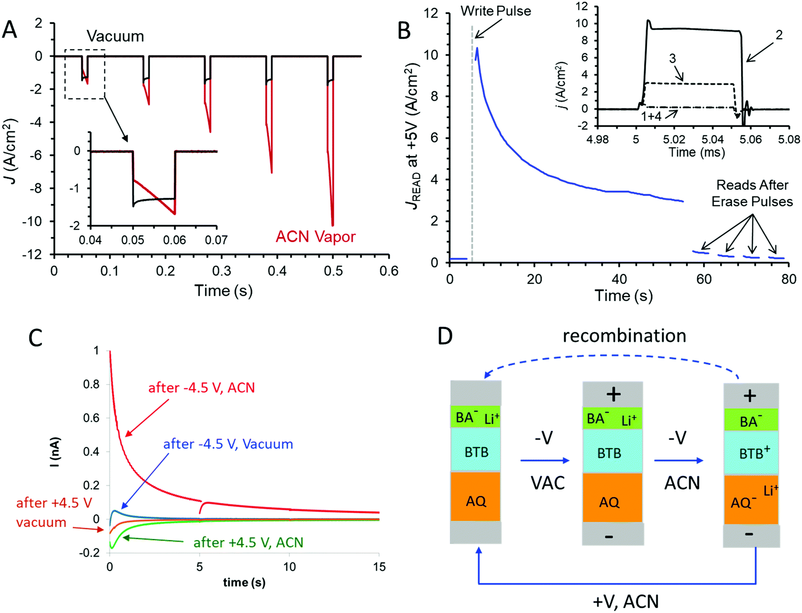 | ||
| Fig. 4 Responses to bias pulses applied to a AQ/BTB/LiBA trilayer device in vacuum and ACN vapour. (A) Current density vs. time during five 10 ms, −4.5 V bias pulses spaced 100 ms apart in vacuum (black trace) and ACN vapour (red trace). Inset shows expanded view of first pulse. (B) J for one thousand +5 V “read” pulses lasting 50 μs spaced 100 ms apart, following a −4.5 V, 10 ms “write” pulse which occurred at t = 5 s. Starting at t = 56 s, four 100 ms, +5 V “erase” pulses were applied which reduced device conductance. Inset shows sample “read” pulses taken before (1), after the −4.5 V “write” pulse (2), 40 seconds later (3), and after the “erase” pulses (4). (C) “Backstep” currents recorded at zero bias following 0.25 s, ±4.5 V bias pulses with the indicated bias values and atmospheres. The discontinuity in the red curve is due to successive 5 second acquisition periods. (D) Schematic of trilayer operation; see text for details. | ||
The possibility of redox reactions and ion motion being involved in the conductance changes in the AQ6.8/BTB8.0/LiBA1.1 trilayer in ACN vapour was investigated by measuring charge flow associated with the “write” pulse. As noted in Fig. 4A, the current during a −4.5 V “write” pulse increases rapidly due to the increased device conductance. If the bias is returned to V = 0 after the “write” pulse, a “backstep” current is observed due to charge motion, with the much larger device current of Fig. 4A absent at zero bias. Fig. 4C shows the backstep current at V = 0 following a 0.25 s, −4.5 V pulse to an AQ6.8/BTB8.0/LiBA1.1 trilayer device (area = 6.25 × 10⁻⁴ cm2) in ACN vapour (red curve). Note that the RC time constant of the junction is a few μs, so the slow current decay is not due to parallel plate capacitance. In addition, positive current on the backstep corresponds to electrons traveling from the bottom electrode (in contact with AQ) to the top electrode (in contact with BTB and LiBA) in the external circuit. The area under the backstep current trace is the total charge leaving the MJ at V = 0 after a “write” pulse, and equals 1.94 × 10⁻⁹ coulombs. Also shown in Fig. 4C is the backstep current observed after a +4.5 V pulse to the same, at-rest device, which is much smaller and corresponds to 2.73 × 10⁻¹⁰ coulombs. In vacuum, the same device shows even smaller backsteps, containing at most to ∼3% of the charge of the backstep from a −4.5 V pulse.
The experimental results support the conclusion that the AQ6.8/BTB8/LiBA trilayer in ACN vapour has properties of a complete redox cell containing two redox systems and mobile ions, combined with “conductance switching” in which the DC current across the MJ is modulated by the charge state of the redox cell. As shown schematically in Fig. 4D, a negative “write” pulse causes reduction of AQ to AQ− and oxidation of BTB to BTB+, accompanied by Li+ motion from the carboxylate group of benzoic acid. Li+ motion stabilizes the space charge generated by the redox reactions to form AQ−/Li+ near the bottom electrode and BTB+/BA− near the top electrode. The relaxation of the “charged” state evident in Fig. 3D and 4B is due to discharge of the redox cell in both the external circuit and at the interface between the AQ and BTB layers. The charge flow upon return to V = 0 after a −4.5 write pulse corresponds to 3.2 × 10⁻¹¹ moles cm−2, which is smaller than that observed for BTB in electrolyte solution29,30 and represents approximately 10% of the total BTB or AQ present in the device. Since BTB+ is a much better electronic conductor than BTB, the 10% change has a large (>100×) effect on device conductance. The similarity of the charge to the total BTB present is also an indication that Li+ insertion into the carbon electrodes is unlikely, and such insertion should occur at both bias polarities if it occurs at all. The backstep results also indicate that there was unintentional reduction of AQ during electrochemical deposition of molecular layers, resulting in a resting state that is slightly charged. An initial positive bias preceding negative “write” pulses oxidizes the AQ− residue and increases the RR. As apparent in Fig. 3D and 4C, the redox cell returns to the slightly charged state after perturbations of either polarity, implying that charge is conserved within the trilayer molecular junction.
The experimental results also clearly indicate a “molecular signature” relating structure to behaviour, plus the ability to drastically change electronic properties in the same external device structure by successive addition of different nanometer-thick molecular layers. We have previously reported several different functions of carbon-based molecular junctions, including tunnelling,6,7,24,41 field ionization,11 emission of light,42–44 photocurrents,45,46 quantum interference,47 audio distortion,22 flexibility23 and rectification.31,48 The current report demonstrates that disparate functions are possible in devices with symmetric contacts by changing molecular structures of one, two or three molecular layers. Some possible applications of such “multifunctional” molecular junctions are listed in Fig. 5, based on past and current results.
 | ||
| Fig. 5 Possible application areas for single layer, bilayer, and trilayer molecular junctions using the same external device structure but different nanometric building blocks. | ||
When the third molecular layer contains mobile Li+, the MJ becomes dynamic, and may be reversibly switched between a ∼15 nm thick molecular rectifier with RR = 240 (@±3.5 V, Fig. 3D, black curve) to a nearly symmetric JV response (RR = 1.2 @±3.5 V, Fig. 3D, green curve), with both cases determined at 1000 V s−1. The reversible, repeatable conductance change can be greater than a factor of 150 (Fig. 3D at V = +4.4 V). Metastable charge storage apparent in Fig. 4 has at least two potential applications in electronics; in memory devices or for on-chip energy storage. The trilayer device has many characteristics of a 16 nm thick “battery”, and could be further improved by positioning the LiBA layer between AQ and BTB to provide the “separator” present in conventional batteries. Li+ motion and redox reactions should permit much higher charge storage density than a standard parallel plate capacitor. High charge density can significantly improve memory devices, with redox cells having higher data density than conventional DRAM, without the need for the process-intense trench capacitor.49 In addition to enabling redox reactions, mobile ions can have dramatic effects on electronic behaviour, such as ionic screening50,51 and internal electric field modification.52–54 The ∼ms dynamics apparent in Fig. 3 should be significantly accelerated for other solid electrolytes, e.g. vapour deposited Nasicon with a conductivity of 0.002 S cm−1![[thin space (1/6-em)]](https://www.rsc.org/images/entities/char_2009.gif) 55 should transit Na+ across 15 nm in <10 ns under a 2 V bias. We anticipate that redox reactions and ion motion, which are absent or actively avoided in silicon microelectronics, may provide useful functions in dynamic molecular junctions.
55 should transit Na+ across 15 nm in <10 ns under a 2 V bias. We anticipate that redox reactions and ion motion, which are absent or actively avoided in silicon microelectronics, may provide useful functions in dynamic molecular junctions.
In conclusion, the results show that it is possible to achieve a variety of electronic functions in a single device structure by variations in the internal structures of 1, 2, or 3 molecular layers with nanometric thicknesses. The functions include a tunnel junction useful in a non-linear amplifier circuit and a bilayer rectifier which yields a different harmonic distribution from the single layer devices. The introduction of mobile Li+ ions into the bilayer rectifier produces a dynamic, redox active device with possible applications in memory and on-chip energy storage. The junction design has sufficient lifetime and temperature tolerance for commercial applications, and further variations of molecular layer order and structure should enable a variety of electronic functions which are difficult or impossible with conventional semiconductor materials.
Conflicts of interest
There are no conflicts to declare.Acknowledgements
The authors thank Adam Bergren for assistance with the music application and Bryan Szeto for assistance with Labview programming and device fabrication. This work was supported by the University of Alberta, the National Research Council of Canada, the Natural Science and Engineering Research Council and Alberta Innovates. ANR (France) is gratefully acknowledged for its financial support (ANR-15-CE09 0001-01).References
- D. Xiang, X. Wang, C. Jia, T. Lee and X. Guo, Chem. Rev., 2016, 116, 4318–4440 CrossRef CAS PubMed.
- R. M. Metzger, Chem. Rev., 2015, 115, 5056–5115 CrossRef CAS PubMed.
- H. B. Akkerman, P. W. M. Blom, D. M. de Leeuw and B. de Boer, Nature, 2006, 441, 69 CrossRef CAS PubMed.
- N. Amdursky, D. Marchak, L. Sepunaru, I. Pecht, M. Sheves and D. Cahen, Adv. Mater., 2014, 26, 7142–7161 CrossRef CAS PubMed.
- C. E. Smith, S. O. Odoh, S. Ghosh, L. Gagliardi, C. J. Cramer and C. D. Frisbie, J. Am. Chem. Soc., 2015, 137, 15732–15741 CrossRef CAS PubMed.
- R. McCreery, H. Yan and A. J. Bergren, Phys. Chem. Chem. Phys., 2013, 15, 1065–1081 RSC.
- A. J. Bergren, R. L. McCreery, S. R. Stoyanov, S. Gusarov and A. Kovalenko, J. Phys. Chem. C, 2010, 114, 15806–15815 CAS.
- L. Luo, L. Balhorn, B. Vlaisavljevich, D. Ma, L. Gagliardi and C. D. Frisbie, J. Phys. Chem. C, 2014, 118, 26485–26497 CAS.
- S. H. Choi, B. Kim and C. D. Frisbie, Science, 2008, 320, 1482–1486 CrossRef CAS PubMed.
- D. Taherinia, C. E. Smith, S. Ghosh, S. O. Odoh, L. Balhorn, L. Gagliardi, C. J. Cramer and C. D. Frisbie, ACS Nano, 2016, 10, 4372–4383 CrossRef CAS PubMed.
- H. Yan, A. J. Bergren, R. McCreery, M. L. Della Rocca, P. Martin, P. Lafarge and J. C. Lacroix, Proc. Natl. Acad. Sci. U. S. A., 2013, 110, 5326–5330 CrossRef CAS PubMed.
- A. Morteza Najarian and R. L. McCreery, ACS Nano, 2017, 11, 3542–3552 CrossRef CAS PubMed.
- K. S. Kumar, R. R. Pasula, S. Lim and C. A. Nijhuis, Adv. Mater., 2016, 28, 1824–1830 CrossRef CAS PubMed.
- Q. Wang, R. Liu, D. Xiang, M. Sun, Z. Zhao, L. Sun, T. Mei, P. Wu, H. Liu, X. Guo, Z.-L. Li and T. Lee, ACS Nano, 2016, 10, 9695–9702 CrossRef CAS PubMed.
- T. A. Su, M. Neupane, M. L. Steigerwald, L. Venkataraman and C. Nuckolls, Nat. Rev. Mater., 2016, 1, 16002 CrossRef CAS.
- L. Venkataraman, J. E. Klare, C. Nuckolls, M. Hybertsen and M. L. Steigerwald, Nature, 2006, 442, 904–907 CrossRef CAS PubMed.
- A. J. Kronemeijer, H. B. Akkerman, T. Kudernac, B. J. V. Wees, B. L. Feringa, P. W. M. Blom and B. D. Boer, Adv. Mater., 2008, 20, 1467–1473 CrossRef CAS.
- D. Wang, D. Fracasso, A. Nurbawono, H. V. Annadata, C. S. S. Sangeeth, L. Yuan and C. A. Nijhuis, Adv. Mater., 2015, 27, 6689–6695 CrossRef CAS PubMed.
- A. Wan, L. Jiang, C. S. S. Sangeeth and C. A. Nijhuis, Adv. Funct. Mater., 2014, 24, 4442–4456 CrossRef CAS.
- C. A. Nijhuis, W. F. Reus and G. M. Whitesides, J. Am. Chem. Soc., 2010, 132, 18386–18401 CrossRef CAS PubMed.
- H. B. Akkerman, A. J. Kronemeijer, J. Harkema, P. A. van Hal, E. C. P. Smits, D. M. de Leeuw and P. W. M. Blom, Org. Electron., 2010, 11, 146–149 CrossRef CAS.
- A. J. Bergren, L. Zeer-Wanklyn, M. Semple, N. Pekas, B. Szeto and R. L. McCreery, J. Phys.: Condens. Matter, 2016, 28, 094011 CrossRef PubMed.
- A. Morteza Najarian, B. Szeto, U. M. Tefashe and R. L. McCreery, ACS Nano, 2016, 10, 8918–8928 CrossRef CAS PubMed.
- H. Yan, A. J. Bergren and R. L. McCreery, J. Am. Chem. Soc., 2011, 133, 19168–19177 CrossRef CAS PubMed.
- M. Supur, S. R. Smith and R. L. McCreery, Anal. Chem., 2017, 89, 6463–6471 CrossRef CAS PubMed.
- F. Anariba, U. Viswanathan, D. F. Bocian and R. L. McCreery, Anal. Chem., 2006, 78, 3104–3112 CrossRef CAS PubMed.
- A. M. Nowak and R. L. McCreery, Anal. Chem., 2004, 76, 1089 CrossRef CAS PubMed.
- J. Ru, B. Szeto, A. Bonifas and R. L. McCreery, ACS Appl. Mater. Interfaces, 2010, 2, 3693–3701 CAS.
- C. Fave, V. Noel, J. Ghilane, G. Trippe-Allard, H. Randriamahazaka and J. C. Lacroix, J. Phys. Chem. C, 2008, 112, 18638–18643 CAS.
- C. Fave, Y. Leroux, G. Trippe, H. Randriamahazaka, V. Noel and J.-C. Lacroix, J. Am. Chem. Soc., 2007, 129, 1890–1891 CrossRef CAS PubMed.
- A. Bayat, J.-C. Lacroix and R. L. McCreery, J. Am. Chem. Soc., 2016, 138, 12287–12296 CrossRef CAS PubMed.
- M. N. Kozicki, M. Park and M. Mitkova, IEEE Trans. Nanotechnol., 2005, 4, 331–338 CrossRef.
- P. C. Lacaze and J.-C. Lacroix, Non-volatile Memories, ISTE Ltd, London, UK, 2014 Search PubMed.
- R. Kumar, R. G. Pillai, N. Pekas, Y. Wu and R. L. McCreery, J. Am. Chem. Soc., 2012, 134, 14869–14876 CrossRef CAS PubMed.
- J. Wu and R. L. McCreery, J. Electrochem. Soc., 2009, 156, P29–P37 CrossRef CAS.
- R. Waser, R. Dittmann, G. Staikov and K. Szot, Adv. Mater., 2009, 21, 2632–2663 CrossRef CAS.
- B. C. Das, B. Szeto, D. D. James, Y. Wu and R. L. McCreery, J. Electrochem. Soc., 2014, 161, H831–H838 CrossRef.
- B. C. Das, R. G. Pillai, Y. Wu and R. L. McCreery, ACS Appl. Mater. Interfaces, 2013, 5, 11052–11058 CAS.
- X. Chen, M. Roemer, L. Yuan, W. Du, D. Thompson, E. del Barco and C. A. Nijhuis, Nat. Nanotechnol., 2017, 12, 797–803 CrossRef CAS PubMed.
- Q. V. Nguyen, P. Martin, D. Frath, M. L. Della Rocca, F. Lafolet, C. Barraud, P. Lafarge, V. Mukundan, D. James, R. L. McCreery and J.-C. Lacroix, J. Am. Chem. Soc., 2017, 139, 11913–11922 CrossRef CAS PubMed.
- S. Y. Sayed, J. A. Fereiro, H. Yan, R. L. McCreery and A. J. Bergren, Proc. Natl. Acad. Sci. U. S. A., 2012, 109, 11498–11503 CrossRef CAS PubMed.
- O. Ivashenko, A. J. Bergren and R. L. McCreery, Adv. Electron. Mater., 2016, 2, 1600351 CrossRef.
- O. Ivashenko, A. J. Bergren and R. L. McCreery, J. Am. Chem. Soc., 2016, 138, 722–725 CrossRef CAS PubMed.
- U. M. Tefashe, Q. V. Nguyen, F. Lafolet, J.-C. Lacroix and R. L. McCreery, J. Am. Chem. Soc., 2017, 139, 7436–7439 CrossRef CAS PubMed.
- J. A. Fereiro, M. Kondratenko, A. J. Bergren and R. L. McCreery, J. Am. Chem. Soc., 2015, 137, 1296–1304 CrossRef CAS PubMed.
- J. A. Fereiro, R. L. McCreery and A. J. Bergren, J. Am. Chem. Soc., 2013, 135, 9584–9587 CrossRef CAS PubMed.
- V. Rabache, J. Chaste, P. Petit, M. L. Della Rocca, P. Martin, J.-C. Lacroix, R. L. McCreery and P. Lafarge, J. Am. Chem. Soc., 2013, 135, 10218–10221 CrossRef CAS PubMed.
- P. Martin, M. L. Della Rocca, A. Anthore, P. Lafarge and J.-C. Lacroix, J. Am. Chem. Soc., 2012, 134, 154–157 CrossRef CAS PubMed.
- Z. Liu, A. A. Yasseri, J. S. Lindsey and D. F. Bocian, Science, 2003, 302, 1543–1545 CrossRef CAS PubMed.
- D. A. Bernards, S. Flores-Torres, H. D. Abruna and G. G. Malliaras, Science, 2006, 313, 1416–1419 CrossRef CAS PubMed.
- J. C. de Mello, N. Tessler, S. C. Graham, X. Li, A. B. Holmes and R. H. Friend, Synth. Met., 1997, 85, 1277–1278 CrossRef CAS.
- D. Braga, N. C. Erickson, M. J. Renn, R. J. Holmes and C. D. Frisbie, Adv. Funct. Mater., 2012, 22, 1623–1631 CrossRef CAS.
- J. H. Cho, L. Jiyoul, X. Yu, K. BongSoo, H. Yiyong, M. J. Renn, T. P. Lodge and C. D. Frisbie, Nat. Mater., 2008, 7, 900–906 CrossRef CAS PubMed.
- X. Yu, Z. Wei, H. Mingjing, C. Jeong Ho, J. R. Michael, H. K. Chris and C. D. Frisbie, Adv. Funct. Mater., 2009, 20, 587–594 Search PubMed.
- D. Horwat and A. Billard, Ionics, 2005, 11, 120–125 CrossRef CAS.
Footnote |
| † Electronic supplementary information (ESI) available. See DOI: 10.1039/c7nh00109f |
| This journal is © The Royal Society of Chemistry 2018 |