
Silicon heterojunction solar cells with effectively transparent front contacts
Rebecca
Saive
 *a,
Mathieu
Boccard
b,
Theresa
Saenz
a,
Sisir
Yalamanchili
a,
Colton R.
Bukowsky
a,
Phillip
Jahelka
a,
Zhengshan J.
Yu
b,
Jianwei
Shi
b,
Zachary
Holman
b and
Harry A.
Atwater
*a
*a,
Mathieu
Boccard
b,
Theresa
Saenz
a,
Sisir
Yalamanchili
a,
Colton R.
Bukowsky
a,
Phillip
Jahelka
a,
Zhengshan J.
Yu
b,
Jianwei
Shi
b,
Zachary
Holman
b and
Harry A.
Atwater
*a
aCalifornia Institute of Technology, Pasadena, CA 91125, USA. E-mail: rebsaive@caltech.edu; haa@caltech.edu
bArizona State University, Tempe, AZ 91125, USA
First published on 27th February 2017
Abstract
We demonstrate silicon heterojunction solar cells with microscale effectively transparent front contacts (ETCs) that redirect incoming light to the active area of the solar cell. Replacing standard contact electrodes by ETCs leads to an enhancement in short circuit current density of 2.2 mA cm−2 through mitigation of 6% shading losses and improved antireflection layers. ETCs enable low loss lateral carrier transport, with cells achieving an 80.7% fill factor. Furthermore, dense spacing of the contact lines allows for a reduced indium tin oxide thickness and use of non-conductive, optically optimized antireflection coatings such as silicon nitride. We investigated the performance of ETCs under varying light incidence angles, and for angles parallel to the ETC lines find that there is no difference in photocurrent density with respect to bare indium tin oxide layers. For angles perpendicular to the ETC lines, we find that the external quantum efficiency (EQE) always outperforms cells with flat contact grids.
Introduction
Solar energy is the most abundant energy source on our planet, and harvesting this resource for large scale electricity generation has been transformed by mass-manufactured silicon photovoltaics. Silicon solar cells lead the photovoltaic market and the price decline for silicon photovoltaic modules has brought us to the point where the module cost constitutes only a minority of the overall cost of a photovoltaic system, placing a premium on efficiency increases as a means to leverage further cost reduction. However, many aspects of silicon photovoltaic technology are maturing, so avenues to meaningful cell efficiency increases are becoming increasingly difficult to realize. The most efficient silicon solar cell technology today is the silicon heterojunction (SHJ)1 which is composed of a high-lifetime crystalline silicon wafer coated with amorphous silicon thin films allowing extremely low surface recombination and selective carrier collection, yielding in turn a high open circuit voltage. Charge carriers that are collected at the front surface need to be transported laterally to the edge of the cell which is then connected to the next cell. As the lateral conductivity of amorphous silicon is too low to allow for good lateral carrier transport, a transparent conductive oxide (TCO) has to be used on the front surface (sun facing side) in addition to a metal grid in order to transport the extracted charge carriers without excessive series resistance losses. The metal grid usually covers around 6% of the active area and therefore leads to losses in short circuit current due to shading.2 A small fraction of these losses is recovered by total internal reflection at the encapsulation layer3 but shading still significantly contributes to the current loss. The TCOs employed to reduce series resistance lead to parasitic absorption and decrease the current further. In order to circumvent these losses, interdigitated back contacts (IBCs) were developed. The charge carriers of both polarities are collected at the rear side of the solar cell which is the side that is facing away from the sun. Moving all electrical contacts to the back comes with the benefit to omit metal grid lines and TCO at the front of the solar cell and therefore optimizes the front surface for optimal optical performance. The highest power conversion efficiency for silicon photovoltaics of 26.3% was achieved using silicon heterojunction solar cells with IBCs.4 Although IBCs can be considered as the best option in terms of optical performance, they are more difficult and expensive to fabricate and a front contact scheme with similar optical properties would be more desirable. Therefore tremendous research effort has been devoted to the development of more transparent TCOs,5–10 metal grids with improved shape,11–16 nanomaterial contacts,17–22 sophisticated encapsulation layer geometries23–25 and other approaches.26,27 In most of these approaches, improved transparency comes at the cost of reduced electrical performance as the sheet resistance increases. Recently, we have developed microscale effectively transparent contacts (ETCs) that redirect the incoming light to the active area due to their triangular cross-section. These ETCs exhibit transparency of up to 99.9% and sheet resistance less than 5 Ω sq−1.28 In this manuscript we report on the integration of effectively transparent contacts with silicon heterojunction solar cells and experimentally find that the current density can be increased by 2 mA cm−2 while achieving 80% fill factor. In contrast, nanowire networks18,20 that provide low sheet resistance to obtain similar fill factors exhibit parasitic plasmon absorption that inherently limits their effective transparency to ∼94%. Microscale grids with flat shape exhibit shading losses corresponding to their geometric coverage.28 The mesoscale contacts presented in this manuscript provide an unprecedented combination of low sheet resistance and near unity effective transparency demonstrated on a realistic solar cell and fabricated with a scalable process.Experimental
Ray optical simulations of silicon heterojunction solar cells with different antireflection coatings and contact layouts were performed using Synopsis LightTools. The spectral and angle dependent transmission of light into the crystalline silicon without contacts were determined using PV Lighthouse's OPAL 2.29 The front surface was set to be planar and custom n-k data which was previously determined by ellipsometry was used as an input for the amorphous silicon, indium tin oxide (ITO) and silicon nitride. Literature values were used for the crystalline silicon30 and the silicon dioxide.31 Reflection, parasitic absorption in the amorphous silicon, ITO, silicon nitride and silicon oxide and transmission into silicon was determined for angles of incidence between 0° and 89° and these values were used as input parameters for the ray optical simulations.Silicon heterojunction (SHJ) solar cells were prepared in the same way as described by S. Y. Herasimenka et al.32 The solar cells had textured back surfaces and flat front surfaces and were fabricated on 270 μm thick 4 inch wafers. These cells were cut to 1.4 cm × 1.4 cm pieces and 7 mm × 7 mm ITO patches defined the active area. Therefore, between different solar cells from the same wafer the only difference in the process was the preparation of the contact layer, potential annealing steps and deposition of antireflection coatings. Five wafers that yielded approximately 30 solar cells each were prepared throughout the course of this project. The results were reproducible and similar for different wafers.33 In this paper we report the results from our fifth wafer, which benefitted from our optimized process conditions. Half of the cells of each wafer were prepared with a layer of 70 nm ITO, the other half with a thinner ITO layer. The cells described in this paper featured an ITO layer of 22 nm. This thickness allowed for optimized dual and triple junction anti reflection coatings. However, we also obtained fill factors of up to 73% for cells with only 9 nm ITO. Flat contacts were fabricated by a standard screen printing process with silver paste.
Effectively transparent contacts were prepared using imprint lithography. Using two-photon lithography triangular cross-section polymer lines were written on silicon substrates. The width of the triangle was 4.5 μm, height 15 μm and period 80 μm. The lines were written to be up to 10 mm long. These samples were used as a mold for the preparation of a PDMS stamps. The PDMS stamps were cut open on both sides of the line grid and put in isopropanol for 6–12 hours in order to obtain a favorable surface energy. Then, the stamp was placed on the ITO patch of the solar cell and silver ink was infilled from the sides via capillary action. This process ensured clean triangular cross-section silver lines without unwanted silver residues between the lines.34
Silicon nitride was deposited in a plasma-enhanced chemical vapor deposition (PECVD) tool at 222 °C, 150 W, 2.5 Torr, 26 sccm silane, 94 sccm ammonia and 575 sccm hydrogen.
The optical constants of the silicon nitride were determined by spectroscopic ellipsometry. First, a sample layer was deposited on a silicon wafer and the layer thickness was determined by etching part of the sample in buffered hydrofluoric acid and measuring the step-height using atomic force microscopy. Then, spectroscopic ellipsometry was used to measure the optical response between 250 and 1200 nm. The layer thickness and ellipsometry then enabled a model-free calculation of the nitride layer's complex index of refraction.
Current–voltage measurements were performed with a xenon lamp and an AM 1.5 filter. The incident power was calibrated with a certified silicon reference cell. An aperture of 5 mm × 6 mm was used for all measured solar cells. This size was chosen as it ensured to measure the largest uniform ETCs contact pattern possible. The short circuit current density does not depend on the aperture size. The open circuit voltage increases with increasing aperture as the ratio between light and dark current becomes more favorable.
Angle- and wavelength-dependent external quantum efficiency measurements were performed using chopped monochromated light from a Fianium supercontinuum laser and a silicon photodiode detector, as described elsewhere. The axis of angular rotation was aligned parallel or perpendicular to the contact finger lines or triangular contacts.
Replacing standard grid lines by effectively transparent contacts
Silicon heterojunction solar cells with 70 nm ITO layers were prepared. Three different contact layouts were compared against each other: (i) an ITO layer with a flat metal grid of 6% surface coverage, (ii) an ITO layer without any metal contact and (iii) an ITO layer with effectively transparent contacts (ETCs). Fig. 1 shows the current–voltage (j–V) characteristics of these three devices. The black curve shows the j–V characteristics of a cell with 70 nm ITO and a flat contact grid. The short circuit current density is 33 mA cm−2 and therefore, 2 mA cm−2 lower than the one of a cell with only the ITO layer and no metallic contacts (blue curve). This corresponds approximately to the 6% shading of the contact grid. The active area of the measured cells was 5 mm × 6 mm. Therefore, a metal contact grid is necessary to provide good lateral transport and cells with only ITO exhibited a low fill factor (59.3%) as can be seen from the blue curve. ETCs on top of the ITO layer (red curve) lead to short circuit current densities comparable to those for cells without any metal contact, which agrees with our previously reported effective contact transparency of up to 99.9%.28 Furthermore, fill factors of up to 80.7% were achieved. With a short circuit current density of 35.0 mA cm−2 and an open circuit voltage of 690 mV, this leads to an efficiency of 19.5%. We performed Suns-Voc measurements of the same devices in which the voltage is measured depending on the light intensity. From these measurements the intrinsic characteristics of a solar cell without losses e.g. through lateral transport can be deduced.35 We obtained a pseudo fill factor of 82.0% showing that the effectively transparent contacts provide excellent lateral conductivity.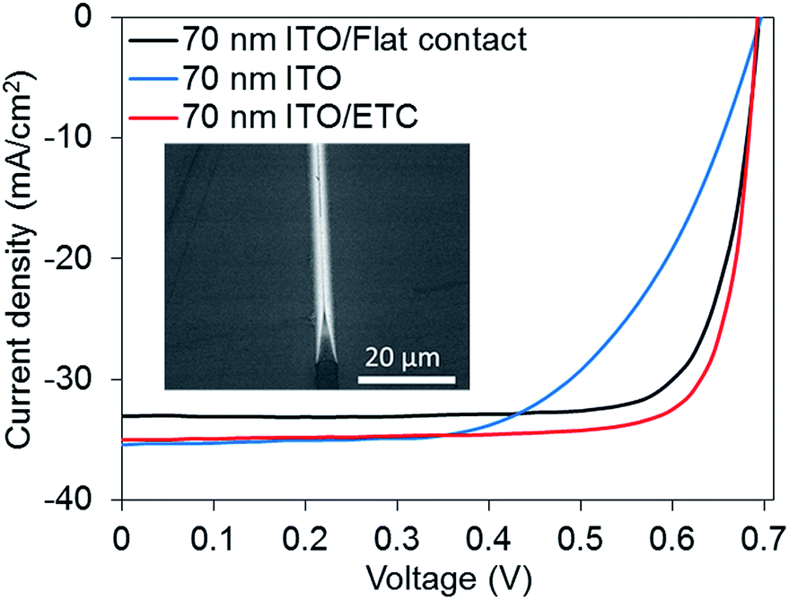 | ||
| Fig. 1 Current–voltage characteristics of silicon heterojunction solar cells with three different front contact. Inset: scanning electron microscope image of a triangular cross-section contact line. | ||
Replacing TCOs by optimized antireflection coatings
One major advantage of ETCs is that their close spacing allows for reduction or even omission of the TCOs that cause parasitic optical absorption. We obtained fill factors of up to 77.2% with only 22 nm-thick ITO and 73.3% with 9 nm-thick ITO. These values are lower than for the thicker ITO because this layout is more sensitive to imperfections: whereas a 70 nm-thick ITO layer can bridge small discontinuities in the lines, cells with thin ITO depend on very good metal grid quality which we think can be achieved in an automated process.We performed optical simulations of the photon transmission into the crystalline silicon in a SHJ solar cell as explained in the method section. Our aim in these simulations is to specifically demonstrate the properties of the contact and antireflection properties without taking into account other properties of the silicon solar cell such as its thickness, back side texture, other light trapping measures or internal quantum efficiency. Fig. 2 shows the spectrum of the light transmitted into the silicon through the metal contacts, the antireflection coatings and the amorphous silicon. Different antireflection coatings and contact layouts are compared with each other: the standard coating without any contacts (70 nm-thick ITO) is shown in blue, 70 nm ITO and a flat contact layout is shown in black and 70 nm ITO and ETCs is shown in red. A cell with ETCs and an antireflection coating consisting of 22 nm ITO/67 nm silicon nitride or 22 nm ITO/43 nm silicon nitride/67 nm silicon oxide is shown in green and purple respectively. The curve for bare 70 nm ITO and ETCs matches closely while the standard flat contacts show lower transmission. An antireflection coating that consists of 22 nm ITO and 67 nm would let less photons through in the shorter wavelength regime but more photons with wavelength longer than around 600 nm. In order to understand this result it must be noted that the ITO we used here (n-k data was measured by ellipsometry) showed low absorption for short wavelength. With an antireflection coating of 22 nm ITO/43 nm silicon nitride/67 nm silicon oxide transmission is enhanced between 300 nm and 450 nm and beyond 600 nm.
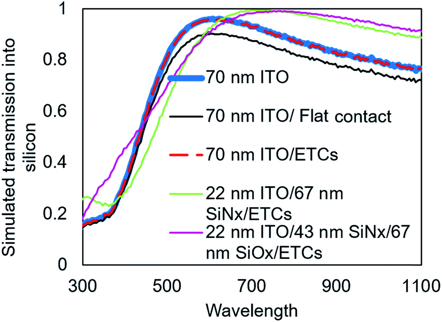 | ||
| Fig. 2 Simulated transmission into the silicon substrate for different contact designs and antireflection coatings. | ||
The plotted quantity corresponds to the photon flux transmitted through the top layers into the crystalline silicon. We can denote a maximum current density which would be achieved if all transmitted photons were absorbed and generated one collected electron hole pair. In reality, not all photons will be absorbed, mostly due to incomplete light trapping and carrier collection for photons with energy close to the band gap of the silicon. Therefore, we expect the experimental external quantum efficiency to be different from this theoretical limit, exhibiting a sharp drop for long wavelengths (cf.Fig. 3). Nonetheless, in order to quantitatively compare the properties of different contact geometries and antireflection coatings, it is instructive to calculate a theoretical short current density for the case in which all photons that transmit through the contact and antireflection layers into the silicon are absorbed and contributed an electron hole pair.
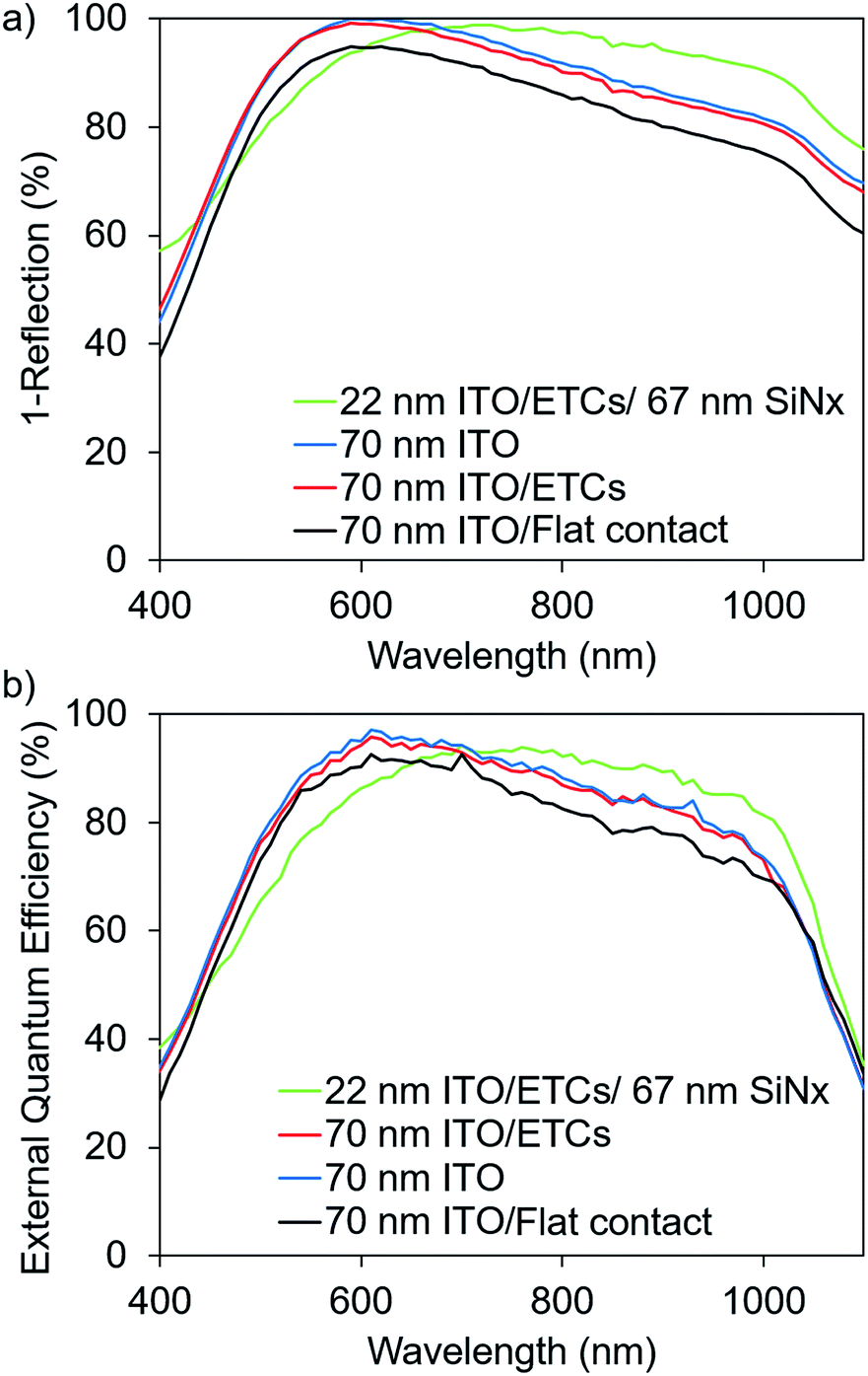 | ||
| Fig. 3 Measured (a) 1-reflection and (b) external quantum efficiency for cells with different front contacts and different antireflection coatings. | ||
We obtain maximum current densities of 36.0 mA cm−2 for 70 nm of ITO without any contact, 35.9 mA cm−2 for 70 nm with ETCs and 33.8 mA cm−2 for 70 nm ITO with standard contacts. A contact that features 22 nm ITO/67 silicon nitride and ETCs transmits photons corresponding to a current density of 37.2 mA cm−2, 22 nm ITO/43 nm silicon nitride/67 nm silicon dioxide leads to a transmission of photons that correspond to a current density of 38.2 mA cm−2. This shows that in addition to the gain from reduced shadow loss, ETCs can enable further current enhancement of around 2 mA cm−2 because they allow for non-conductive antireflection coatings.
Fig. 3a shows the result from measurements of the wavelength dependent reflectance for samples with different antireflection coatings and contact layouts. A cell with a bare ITO front contact is shown in blue, a cell with ITO and flat screen printed contacts in black, a cell with ITO and ETCs in red and a cell with 22 nm ITO/ETCs/67 nm silicon nitride is shown in green. As expected from the optical simulations the reflectance of a cell with 70 nm ITO is barely affected by adding ETCs. Unsurprisingly, adding flat contacts increases the reflectance. Using an antireflection coating of 22 nm ITO and 67 nm silicon nitride decreases the reflectance significantly for wavelengths greater than 600 nm as well as for short wavelengths as predicted by optical simulations.
We also performed external quantum efficiency (EQE) measurements for these cells. Fig. 3b shows the EQE for a cell with a bare ITO front contact (blue curve), a cell with ITO and flat screen printed contacts (black curve), a cell with ITO and ETCs (red curve) and a cell with 22 nm ITO/ETCs/67 nm silicon nitride. Bare ITO and ITO with ETCs gives similar results while flat contacts give a lower EQE over the whole spectrum as one would expect. If the 70 nm ITO is replaced by 22 nm ITO and 67 silicon nitride we observe lower absorption for shorter wavelengths and higher absorption for longer wavelengths. This is expected from the simulation of the transmission through the front contacts and also from the data of Fig. 3a.
Table 1 summarizes the short circuit current density (jsc), the open circuit voltage (Voc), the fill factor (FF) and the efficiency (η) for the SHJ solar cells with different front contacts and antireflection coatings.
| 70 nm ITO/flat contacts | 70 nm ITO | 70 nm ITO/ETCs | 22 nm ITO/ETCs/67 nm SiNx | |
|---|---|---|---|---|
| V oc (mV) | 693 | 697 | 690 | 687 |
| j sc (mA cm−2) | 33.0 | 35.4 | 35.0 | 35.6 |
| FF (%) | 79.0 | 59.3 | 80.3 | 73.8 |
| η (%) | 18.1 | 14.6 | 19.5 | 18.1 |
Angular performance of ETCs
Simulations and measurements of the angle dependent transmission of ETCs compared to flat contacts or bare ITO layers show a spectrally broad and surprisingly angle-insensitive response. Fig. 4a–d show the simulated transmission of photons into the crystalline silicon absorber layer for SHJ solar cells with (a) bare ITO, (b) ITO with flat contacts, (c) ITO and ETCs where the angle β is varied parallel to the grid lines and (d) ITO and ETCs where the angle α is varied perpendicular to the grid lines. A bare ITO contact shows greater transmission for increasing angle over a major part of the wavelength spectrum as the thickness of the ITO is optimized for optimal antireflection properties under normal incidence. Therefore a deviation from normal incidence increases the reflection and lowers the transmission. If a flat contact grid is assumed, the overall transmission drops for all wavelengths. If ETCs are assumed, and the angle is varied parallel to the contact lines a similar behavior as for bare ITO is observed.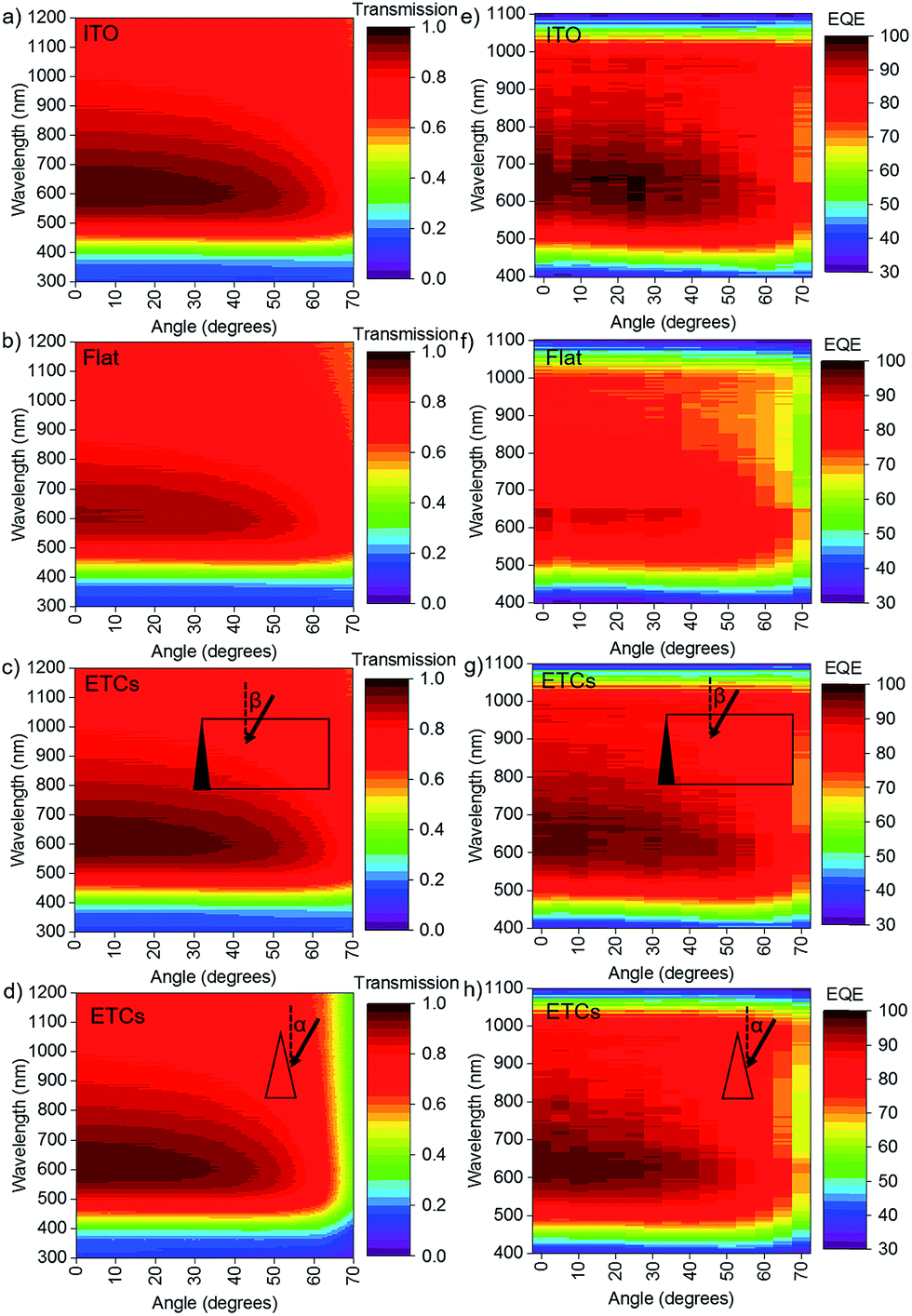 | ||
| Fig. 4 a)–(d) Simulated transmission into silicon and (e)–(h) measured external quantum efficiency depending on the angle of incidence and wavelength for front contacts with (a and e) bare ITO, (b and f) ITO and flat contacts, (c and g) ETCs (angle varied parallel to the lines) and (d and h) ETCs (angle varied perpendicular to the lines). | ||
We also performed angle and wavelength dependent EQE measurements of SHJ solar cells. These are shown in Fig. 4e–h; (e) a bare ITO front contact, (f) ITO with flat contacts and (g and h) ITO with ETCs where the angle was scanned parallel and perpendicular to the contact lines respectively. For all cells we obtain low EQE for all angles for the shortest and longest wavelength as already observed at normal incidence. ITO with flat contacts give an overall lower EQE. The EQE of ETCs where the angle is varied parallel to the contact lines is similar to the case with bare ITO.
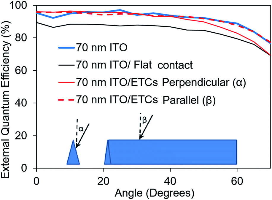
Fig. 5 shows the angle dependent EQE for incident photons with a wavelength of 600 nm. The angle dependence of the EQE of a cell with bare ITO front contact is shown in blue. The EQE decreases with increasing angle of incidence as the thickness of the ITO is optimized to provide optimal antireflection properties for photons with normal incidence. The EQE dependence of a cell with ITO and ETCs where the angle is varied parallel to the ETCs (angle β in Fig. 5) is shown as dashed red curve. The curve follows the behavior of pure ITO. Changing the angle perpendicular to the ETCs (α in Fig. 5) leads to a slight drop in EQE beyond 40° angle of incidence as seen by the solid red curve. However even with light incident perpendicular to the ETCs, the EQE is always higher than for a cell with flat contacts (black curve in Fig. 5). These results show that there is no reduction in acceptance resulting from the ETCs for angles of incidence parallel to the ETCs and only minor reduction for angles of incidence perpendicular to the ETCs beyond 40°. In a field of photovoltaic modules, angle dependent EQE losses might be avoided by mounting the modules such that the lines are oriented horizontally.
 | ||
| Fig. 5 Measured angle dependence of the external quantum efficiency for different front contact designs at 600 nm incident photon wavelength. | ||
Conclusion
We have demonstrated effectively transparent contacts (ETCs) that enhance the short circuit current density of SHJ solar cells by avoiding shadow losses. Furthermore, these contacts can be placed close together such that more optimal non-conductive antireflection coatings can be used. ETCs feature an acceptance angle range similar to that for bare antireflection coatings if the incidence angle plane is parallel to the contact lines. Perpendicular to the contact lines the external quantum efficiency starts dropping off for angles beyond 40°.Effectively transparent contacts represent a general approach to light management, and are not limited to a specific solar cell technology. Advanced printing technologies may enable a pathway to scale-up for use with mass-manufactured photovoltaics. We have previously demonstrated ETC printing on top of textured Si surfaces, suggesting a path to ETC contact use with textured Si solar cells.28 The challenge is to prepare a stamp that prevents ink from flowing in between the lines while being stiff enough to maintain shape. Due to their close spacing, ETCs could in principle also allow omission of TCO thin films altogether as it is also the case for other micro- and nanogrids. Thus we can anticipate that optimized ETC designs could add more than 2 mA cm−2 additional short circuit density to a variety of state-of-the art front-contacted cells, leading to efficiency improvements of around 1% absolute.
Acknowledgements
This material was based upon work supported by the U.S. Department of Energy through the Bay Area Photovoltaic Consortium under Award Number DE-EE0004946. Authors and their work presented herein are funded in part by the Department of Energy, Energy Efficiency and Renewable Energy Program, under Award Number DE-EE0006335. This material is based upon work supported by the Engineering Research Center Program of the National Science Foundation and the Office of Energy Efficiency and Renewable Energy of the Department of Energy under NSF Cooperative Agreement No. EEC-1041895. Any opinions, findings and conclusions or recommendations expressed in this material are those of the authors and do not necessarily reflect those of the National Science Foundation or Department of Energy.References
- M. Tanaka, et al., Development of new a-Si/c-Si heterojunction solar cells: ACJ-HIT (artificially constructed junction-heterojunction with intrinsic thin-layer), Jpn. J. Appl. Phys., 1992, 31, 3518 CrossRef CAS.
- P. A. Basore et al. , in 2013 IEEE 39th Photovoltaic Specialists Conference (PVSC), IEEE, 2013, pp. 0900–0903 Search PubMed.
- A. Blakers, Shading losses of solar-cell metal grids, J. Appl. Phys., 1992, 71, 5237–5241 CrossRef CAS.
- http://www.kaneka.co.jp/kaneka-e/images/topics/1473811995/1473811995_101.pdf, 2016.
- K. M. Yu, et al., Ideal transparent conductors for full spectrum photovoltaics, J. Appl. Phys., 2012, 111, 123505 CrossRef.
- M. Morales-Masis, S. M. De Nicolas, J. Holovsky, S. De Wolf and C. Ballif, Low-temperature high-mobility amorphous IZO for silicon heterojunction solar cells, IEEE Journal of Photovoltaics, 2015, 5, 1340–1347 CrossRef.
- T. Koida, H. Fujiwara and M. Kondo, High-mobility hydrogen-doped In2O3 transparent conductive oxide for a-Si: H/c-Si heterojunction solar cells, Sol. Energy Mater. Sol. Cells, 2009, 93, 851–854 CrossRef CAS.
- L. Barraud, et al., Hydrogen-doped indium oxide/indium tin oxide bilayers for high-efficiency silicon heterojunction solar cells, Sol. Energy Mater. Sol. Cells, 2013, 115, 151–156 CrossRef CAS.
- E. Kobayashi, Y. Watabe, T. Yamamoto and Y. Yamada, Cerium oxide and hydrogen co-doped indium oxide films for high-efficiency silicon heterojunction solar cells, Sol. Energy Mater. Sol. Cells, 2016, 149, 75–80 CrossRef CAS.
- K. Ellmer, Past achievements and future challenges in the development of optically transparent electrodes, Nat. Photonics, 2012, 6, 809–817 CrossRef CAS.
- S. R. Wenham and M. A. Green. Electrical contact formed in groove in surface or semiconductor, US Pat., US 4726850 A, 1988.
- J. Schneider, et al., Combined effect of light harvesting strings, anti-reflective coating, thin glass, and high ultraviolet transmission encapsulant to reduce optical losses in solar modules, Prog. Photovoltaics, 2014, 22, 830–837 Search PubMed.
- E. M. Sachs, J. Serdy, A. Gabor, F. Van Mierlo and T. Booz. in Proceedings of the 24th European Photovoltaic Solar Energy Conference and Exhibition, 4CO, 2009 Search PubMed.
- J. S. Ward, et al., High aspect ratio electrodeposited Ni/Au contacts for GaAs-based III–V concentrator solar cells, Prog. Photovoltaics, 2015, 23, 646–653 CAS.
- P. Kuang, et al., A New Architecture for Transparent Electrodes: Relieving the Trade-Off Between Electrical Conductivity and Optical Transmittance, Adv. Mater., 2011, 23, 2469–2473 CrossRef CAS PubMed.
- H. Hauser, et al., Development of nanoimprint processes for photovoltaic applications, J. Micro/Nanolithogr., MEMS, MOEMS, 2015, 14, 031210 CrossRef.
- Q. Zheng, Z. Li, J. Yang and J.-K. Kim, Graphene oxide-based transparent conductive films, Prog. Mater. Sci., 2014, 64, 200–247 CrossRef CAS.
- J. van de Groep, P. Spinelli and A. Polman, Transparent Conducting Silver Nanowire Networks, Nano Lett., 2012, 12, 3138–3144, DOI:10.1021/nl301045a.
- J. van de Groep, et al., Large-area soft-imprinted nanowire networks as light trapping transparent conductors, Sci. Rep., 2015, 5, 11414 CrossRef PubMed.
- P.-C. Hsu, et al., Performance enhancement of metal nanowire transparent conducting electrodes by mesoscale metal wires, Nat. Commun., 2013, 4, 2522 Search PubMed.
- F. Afshinmanesh, A. G. Curto, K. M. Milaninia, N. F. van Hulst and M. L. Brongersma, Transparent metallic fractal electrodes for semiconductor devices, Nano Lett., 2014, 14, 5068–5074 CrossRef CAS PubMed.
- V. K. Narasimhan, T. M. Hymel, R. A. Lai and Y. Cui, Hybrid Metal–Semiconductor Nanostructure for Ultrahigh Optical Absorption and Low Electrical Resistance at Optoelectronic Interfaces, ACS Nano, 2015, 9, 10590–10597 CrossRef CAS PubMed.
- P. Jahelka, R. Saive and H. Atwater, Total Internal Reflection for Effectively Transparent Solar Cell Contacts, arXiv preprint arXiv:1610.01047, 2016.
- F.-h. Chen, S. Pathreeker, J. Kaur and I. D. Hosein, Increasing light capture in silicon solar cells with encapsulants incorporating air prisms to reduce metallic contact losses, Opt. Express, 2016, 24, A1419–A1430 CrossRef PubMed.
- J. M. Rodriguez-Parada, R. J. Riegert, M. E. Lewittes and R. H. French, US Pat., US8441735 B2, 2013.
- M. F. Schumann, et al., Cloaked contact grids on solar cells by coordinate transformations: designs and prototypes, Optica, 2015, 2, 850–853 CAS.
- P. G. Kik, Catoptric electrodes: transparent metal electrodes using shaped surfaces, Opt. Lett., 2014, 39, 5114–5117 CrossRef PubMed.
- R. Saive, et al., Effectively Transparent Front Contacts for Optoelectronic Devices, Adv. Opt. Mater., 2016, 4(10), 1470–1474 CrossRef CAS.
- K. R. McIntosh and S. C. Baker-Finch, OPAL 2: Rapid optical simulation of silicon solar cells, Proceedings of the 38th IEEE Photovoltaic Specialists Conference, Austin, 2012 Search PubMed.
- M. A. Green, Self-consistent optical parameters of intrinsic silicon at 300 K including temperature coefficients, Sol. Energy Mater. Sol. Cells, 2008, 92, 1305–1310 CrossRef CAS.
- E. D. Palik. Handbook of optical constants of solids, Academic press, 1998, vol. 3 Search PubMed.
- S. Y. Herasimenka, W. J. Dauksher and S. G. Bowden, > 750 mV open circuit voltage measured on 50 μm thick silicon heterojunction solar cell, Appl. Phys. Lett., 2013, 103, 053511 CrossRef.
- R. Saive et al. , in Photovoltaic Specialists Conference (PVSC), IEEE 43rd, 2016, pp. 3612–3615 (IEEE) Search PubMed.
- R. Saive, C. R. Bukowsky and H. Atwater, Three-dimensional nanoimprint lithography using two-photon lithography master samples. arXiv preprint arXiv:1702.04012v1, 2017.
- R. Sinton and A. Cuevas, in Proceedings of the 16th European Photovoltaic Solar Energy Conference, 2000 Search PubMed.
| This journal is © The Royal Society of Chemistry 2017 |