
Enhanced morphology and stability of high-performance perovskite solar cells with ultra-smooth surface and high fill factor via crystal growth engineering†
Jiajiu
Ye
ab,
Xuhui
Zhang
b,
Liangzheng
Zhu
b,
Haiying
Zheng
b,
Guozhen
Liu
ab,
Hongxia
Wang
 d,
Tasawar
Hayat
c,
Xu
Pan
*b and
Songyuan
Dai
*ac
d,
Tasawar
Hayat
c,
Xu
Pan
*b and
Songyuan
Dai
*ac
aState Key Laboratory of Alternate Electrical Power System with Renewable Energy Sources, North China Electric Power University, Beijing 102206, China. E-mail: sydai@ipp.ac.cn; xpan@rntek.cas.cn
bKey Laboratory of Novel Thin-Film Solar Cells, Institute of Applied Technology, Hefei Institutes of Physic Science, Chinese Academy of Sciences, Hefei 230031, China. E-mail: xpan@rntek.cas.cn
cDepartment of Mathematics, Faculty of Science, King Abdulaziz University, Jeddah 21589, Saudi Arabia
dSchool of Chemistry, Physics and Mechanical Engineering, Queensland University of Technology, Brisbane, QLD 4001, Australia
First published on 14th March 2017
Abstract
Since solvent engineering methods were applied to the treatment of perovskite films, the performance of perovskite solar cells (PSCs) has shown rapid growth and remarkable achievements have been made. Here we report a highly reproducible method for controlling perovskite crystal growth by a spraying anti-solvent process, which is quite different from conventional dripping methods. The results showed that the change of the method by which the anti-solvent is used has a significant impact on the morphology and formation of the perovskite. It has a high probability to form a mirror-like surface without wave-circle or ring defects, and to obtain a longer carrier lifetime than crystals formed by by dripping. After optimizing the spraying operating conditions, the optimal device based on FA0.81MA0.15Cs0.025PbI2.5Br0.45 obtained a PCE of 19.21%. Particularly, this method exhibited good reproducibility and a high fill factor due to the reduced crystal defects in the film. The champion cell obtained a fill factor as high as 80.84%, measured at AM 1.5G, 100 mW cm−2. It is expected that these findings can be beneficial for the future integrated applications of these perovskites.
1 Introduction
Organic–inorganic perovskites have shown one of the most rapid growths ever in photovoltaic history since Miyasaka and co-workers reported perovskite solar cells (PSCs) for the first time in 2009.1–4 To achieve high-quality perovskite films, many research efforts have contributed to various film deposition approaches based on lead organo-halide perovskites such as sequential deposition,5,6 screen printing,7 vapor-assisted,8 co-evaporation of the precursors9,10 and near-space sublimation etc.11 Meanwhile, several strategies have been used to increase the quality of perovskite films, including a wide range of compositions for precursor solutions,12 additives like HX,13 gas-assisted methods,14 microwave irradiation processes,15 laser-assisted crystallization16 and high-temperature treatment.17In 2014, Seok and coworkers introduced a solvent-engineering method by dripping anti-solvent to fabricate PSCs, through which, the morphology of the perovskite film can be controlled easily, and they achieved a PCE exceeding 16.2%. This technology has been widely used in one-step deposition methods.18 However, it inevitably produces perovskite films with a relatively rough and pinhole-rich surface when the anti-solvent amount, timing of dripping, the ambient operating environment and the spin coating speed were not suitable, which are unacceptable in PSCs. As a result, there will often occur a phenomenon in which the perovskite film surface will appear uneven, rough, and circled with wave-like ripples, or even cracked which is particularly evident in large scale devices.19 This can result in serious perovskite crystal disorder, excessive grain boundaries and recombination between electrons and holes, leading to a large current leakage as well as a low fill factor (FF).20,21
This is probably caused by two main factors: the solvent evaporation rate and the impact force of anti-solvent droplets. The precursor solvent evaporates quickly and is extruded out when superfluous anti-solvent is added. The film loses the support solvent which keeps the smooth integrity of the surface and thus results in film cracking, which can be seen visually. In contrast, too little anti-solvent causes it to lose the ability to squeeze the precursor solvent and promote crystal growth, and finally leads to a rough surface.22 On the other hand, an inappropriate dripping time or improper rotation speed can also cause an imbalance between the solvent evaporation rate and the crystal growth process. Another important limitation of the solvent engineering method is the dripping impact force. When the anti-solvent lands on the substrate, it has a greater chance to produce a damaged film with circles in the shape of waves or cracks. It is impossible to produce large-area film substrates by dripping owning to the small area of anti-solvent drop dot.23
Moreover, due to the drops of anti-solvent being operated manually, it is not possible for the dropping rate, dropping angle, and dropping height to be exactly the same every time. These simple operational details have a direct impact on the morphology of the perovskite film. In order to reduce the effects of drop impact and the fragile solvent evaporation balance, we adopted a spraying anti-solvent process which has a highly uniform consistency and can be easily controlled even when used by different researchers.24
Spray technology is a commonly used technique which has been used to deposit many kinds of thin films in the past decades. Recently, some works have reported the deposition of perovskite solar cells using this technique to fabricate the blocking layer, light absorbing materials and the hole transport layer.25,26 Differently from previous approaches with the purpose of deposition, we used this technology to atomize the anti-solvent. When the anti-solvent contacts the substrate, the atomized solvent particles are evenly dispersed. This reduces negative effects caused by the impact and centrifugal force, as illustrated in Fig. 1. An outward flux of the precursor solvents was generated, while the perovskite began to nucleate and crystallize. The crystallization process from the bottom to the top of the perovskite film has a correlation with continuous spraying conditions. By continuously supplying anti-solvent, the small, initially formed perovskite crystal grains can be grown into larger crystals.27–29
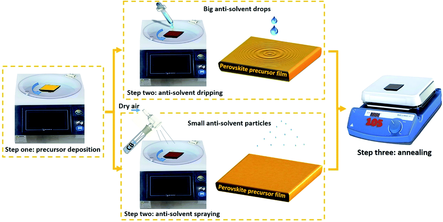 | ||
| Fig. 1 Schematic diagram of the spraying anti-solvent process (SAP) and the conventional dripping method. The anti-solvent was sprayed onto the perovskite/TiO2/FTO substrate. Dripping anti-solvent onto the substrate generates an impact force. In contrast, SAP can produce uniformly dispersed small particles, and the rate is controllable via the carrier gas flow rate. | ||
In this article, we report a highly reproducible method for controlling perovskite crystal growth by spraying anti-solvent, which is quite different from the conventional dripping method. The device was based on a FTO/bl-TiO2/meso-TiO2/perovskite/spiro/Au architecture. The change of the method by which the anti-solvent is used has a significant impact on the morphology and formation process of the perovskite. The anti-solvent contacts the film more softly and uniformly, which effectively reduces waves and eliminates ring defects in the perovskite film. It was found that a smooth surface without film cracking or wave-circle film surface can be obtained by the spraying anti-solvent process (SAP). The gas flow rate, spraying time and spinning coating speed were critical for film crystallization. The resulting film showed enhanced carrier transport properties compared to films made by conventional methods. The film prepared by dripping displayed a carrier lifetime of 175.81 ns, longer than that of the defect film which was 118.58 ns. After optimizing the spraying operating conditions, the power conversion efficiency was increased from 15.34% to 18.78%, and the optimal devices based on the FA0.81MA0.15Cs0.025PbI2.5Br0.45 light absorber obtained a record PCE of 19.21% with a FF as high as 80.84% measured under conditions of AM 1.5G 100 mW cm−2. In particular, this method exhibited good reproducibility and high FF due to the reduction of crystal defects in the film. It is expected that these findings can be beneficial for large scale area perovskite solar cells and future integrated applications.
2 Materials and methods
2.1 Materials
Lead(II) iodide (99.99%, trace metals basis), for the perovskite precursor, was purchased from TCI; CH3NH3I, MABr and spiro-MeOTAD from Xi’an Polymer Light Technology Corp. Ltd; TiO2 (particle size: about 30 nm, crystalline phase: anatase) from Dysol; DMF, chlorobenzene, lithium bis(trifluoromethylsulphonyl) imide (Li-TFSI) and 4-tert-butylpyridine (tBP) from Aldrich; and CsI from Alfa. All chemicals were directly used without further purification. Patterned FTO-coated glass substrates with a sheet resistance of 15 ohm sq−1 were cleaned sequentially by ultrasonication in mild detergent, deionized water, acetone and ethanolamine. The substrates were exposed to UV-ozone for 20 min prior to the spin coating step. The spray equipment consists of a solution dispersion system with a 10 ml container, a compressor to provide spray droplet carrier air flow, a glass nozzle and air flow as a pump to manage delivery of the solution from the dispersion container into the spray nozzle. A pressure-regulating valve sets the carrier air pressure before entering into the nozzle (0.3 MPa). The nozzle-tip-to-substrate distance was kept constant at 60–100 mm, and the carrier air speed was set at 90 l h−1. Fig. 1 exhibits a schematic of the spray coating system.2.2 Solar cell device fabrication
A thick, dense blocking layer of TiO2 (bl-TiO2) was deposited onto an F-doped SnO2 (FTO) substrate by spin coating to prevent direct contact between the FTO and the hole-conducting layer. A TiO2 blocking layer was deposited on the cleaned FTO by spray pyrolysis, using dry air as carrier gas, at 460 °C from a precursor solution of 0.6 ml of titanium diisopropoxide and 0.4 ml of bis(acetylacetonate) in 7 ml of anhydrous isopropanol. A mesoporous TiO2 layer (Dysol, particle size: about 30 nm, crystalline phase: anatase; diluted to w/w = 1/6 in ethanol) of about 160–180 nm thickness film was deposited by spin coating at 4000 rpm for 20 s onto the bl-TiO2/FTO substrate. After spin coating, the substrate was immediately dried on a hotplate at 120 °C, and the substrates were then calcined at 510 °C to remove the organic components. The perovskite film was deposited by spin coating onto the TiO2 substrate. The prepared FAI powders and PbI2 (TCI) for FA0.81MA0.15Cs0.025PbI2.5Br0.45 solution (1.4 M Pb+) were stirred in a mixture of DMSO and DMF (v/v = 2![[thin space (1/6-em)]](https://www.rsc.org/images/entities/char_2009.gif) :8) at 60 °C for complete dissolution. The precursor solution was prepared in a glovebox of 1.4 M Pb2+ (PbI2 and PbBr2) in a mixed solvent of DMF and DMSO, the volume ratio of DMF to DMSO was 4:1. The molar ratio for PbI2/PbBr2 was fixed at 0.85:0.15, PbI2/FAI was fixed at 1.05, FAI/CsI was fixed at 32.4, and the molar ratio for MABr/PbBr2 was fixed at 1:1. The resulting solution was coated onto the mp-TiO2/bl-TiO2/FTO substrate by a consecutive two-step spin-coating process at 1100 and 5000 rpm for 10 s and 60 s, respectively. During the second spin-coating step at 20 s, the substrate was treated with the anti-solvent (chlorobenzenel) by the spraying method and this lasted for 20 s to form the perovskite crystal; the substrate was then heated at 105 °C for 1 h on a hotplate under low-speed flow, clean, dry air protection. FAI was synthesized from hydroiodic acid reacting with formamidine acetate. The HTM layer was deposited by spin-coating at 4000 rpm for 20 s, using a solution of spiro-MeOTAD, 4-tert-butylpyridine, lithium bis(trifluoromethylsulphonyl) imide and the Co(III)-complex. Finally, the gold (80 nm) counter electrode was deposited by thermal evaporation on top of the device to form the back contact.
:8) at 60 °C for complete dissolution. The precursor solution was prepared in a glovebox of 1.4 M Pb2+ (PbI2 and PbBr2) in a mixed solvent of DMF and DMSO, the volume ratio of DMF to DMSO was 4:1. The molar ratio for PbI2/PbBr2 was fixed at 0.85:0.15, PbI2/FAI was fixed at 1.05, FAI/CsI was fixed at 32.4, and the molar ratio for MABr/PbBr2 was fixed at 1:1. The resulting solution was coated onto the mp-TiO2/bl-TiO2/FTO substrate by a consecutive two-step spin-coating process at 1100 and 5000 rpm for 10 s and 60 s, respectively. During the second spin-coating step at 20 s, the substrate was treated with the anti-solvent (chlorobenzenel) by the spraying method and this lasted for 20 s to form the perovskite crystal; the substrate was then heated at 105 °C for 1 h on a hotplate under low-speed flow, clean, dry air protection. FAI was synthesized from hydroiodic acid reacting with formamidine acetate. The HTM layer was deposited by spin-coating at 4000 rpm for 20 s, using a solution of spiro-MeOTAD, 4-tert-butylpyridine, lithium bis(trifluoromethylsulphonyl) imide and the Co(III)-complex. Finally, the gold (80 nm) counter electrode was deposited by thermal evaporation on top of the device to form the back contact.
2.3 Characterization
The PCE and J–V curves were measured by using a solar simulator (Newport, Oriel Class A, 91195A) with a source meter (Keithley 2420) at 100 mW cm−2 illumination AM 1.5G and a calibrated Si-reference cell certified by NREL. The J–V curves for all devices were measured by masking the active area with a black mask 0.09 cm2. Incident photon-to-current efficiencies (IPCE) were confirmed as a function of wavelength from 300 to 800 nm (PV Measurements, Inc.) with a dual xenon/quartz halogen light source, measured in DC mode with no bias light used. The setup was calibrated with a certified silicon solar cell (Fraunhofer ISE) prior to measurements. Film morphology was investigated by using polarizing microscope and a high-resolution scanning electron microscope equipped with a Schottky field emission gun. PL spectra were recorded by exciting the perovskite films deposited onto mesoporous TiO2 at 490 nm with a standard 450 W xenon CW lamp. The signal was recorded by a spectrofluorometer (Photon Technology International) and analyzed by fluorescence software. Transient absorption spectra (TAS) were recorded on an LKS (Applied Photophysics). The cells were measured before evaporating a gold counter with a pump light wavelength of 500 nm and a probe light wavelength of 775 nm. The repetition rate was 5 Hz and the energy of the laser device was 150 μJ cm−2.3 Result and discussion
It is crucial for devices to obtain a flat perovskite layer with a fully and homogenously covered surface. Herein, we adopted spraying anti-solvent technology as an effective method for preparing such a layer. Fig. 1 presents a schematic diagram of the spraying process and the dripping method.The spraying anti-solvent process (SAP) was performed in two steps. Firstly, the perovskite film was deposited via spin-coating. Secondly, the anti-solvent was sprayed on the film, thus it can be rapidly dispersed in the whole film and greatly alleviate the negative effects caused by the liquid drop impact-force and the rotating centrifugal force. The pristine chlorobenzene and precursor solvent have good affinity, so the solvent can evaporate rapidly. We deduced that the SAP could be beneficial for the quick and gentle removal of the solvent, which induces the perovskite to form a more uniform and flat high-quality film. Finally, the homogeneous flat film was converted into a smooth and shiny perovskite layer after annealing.
It was found that the film quality has a close correlation with the carrier gas flow rate, the spinning coating speed and the spraying time. It is likely that films with uncovered or poor crystallinity will be obtained under inappropriate operating conditions. In particular, the stability of the carrier air flow is important. After a series of experiments, a smooth and reflective perovskite film can be obtained at 4500 rpm by spraying for 20 s (gas flow rate was 90 l min−1). Detailed parameters are shown in Table S1.†
As the perovskite film morphology and surface coverage are crucial to the performance, a polarizing microscope was used to examine the film surface. As illustrated in Fig. 2(a) and (b), the film was prepared by the conventional dripping anti-solvent method. Near the central area where the drops landed, there can be seen clearly large voids and extremely rough surfaces with circles distributed in the film. Although a flat film can usually be obtained by skilled technical personnel, defective films are sometimes inevitable. For further observation, we investigated the morphology of the annular raised portion by SEM. We can see waves and ravines throughout the whole film in Fig. 2(c). As a result, HTM will penetrate into the interior of the perovskite layer and will cause serious recombination between large numbers of charge carriers. Fig. 2(d)–(i) show the morphology of perovskite films prepared by the SAP method under different conditions. It can be observed that the surface of the films exhibited an island of non-uniform coverage. As the carrier gas flow rate, spinning coating speed and spraying time have a direct impact on the morphology, improper conditions will always produce an uncovered or rough surface. The chlorobenzene droplet particles will quickly react with the solvent after sufficient diffusion on the film surface. The size of the droplets particles was influenced significantly by the spray speed, the nozzle size, the space distance between the nozzle and substrate, and so on. Too-great a carrier gas flow rate will produce a larger gas blowing force and a high speed of the anti-solvent; the integrity of film would accordingly be destroyed, which will lead to an uncovered surface, as shown in Fig. 2(d) and (g). In contrast, a too-small flow rate generates heterogeneous droplets and particles which cause the films to become uneven, Fig. 2(e) and (h). After selection of the preparation parameters obtained appropriate conditions (Table S1† and Fig. 1), a smooth and flat film can be produced with bigger crystal grains as shown in Fig. 2(f, i and j). The film exhibited a shiny surface and uniform nanocrystals, almost no voids and cracks can be seen in many films prepared using the same process. It was clearly observed that the surface structure of films after the dripping and spraying process showed no significant change (SEM images of film morphology prepared by dripping method are shown in Fig. S2†), whereas the difference was that sectional morphology of the SAP method showed a flat perovskite layer and high quality crystallization. It can be inferred that the carrier loss at grain boundaries or structural defects is decreased, and the generated charges can reach the electrodes without recombination. These results confirm the previous speculation that the uniformity of diffuse anti-solvent, instead of larger drops, can cause perovskite films to become more uniform and flat. Therefore, this could reduce defect states and enhance the intrinsic stability of the perovskite itself. The crystallinity of the perovskite films was closely related to the performance of the final device, and the positive effect on photovoltaic performance has already been confirmed.30
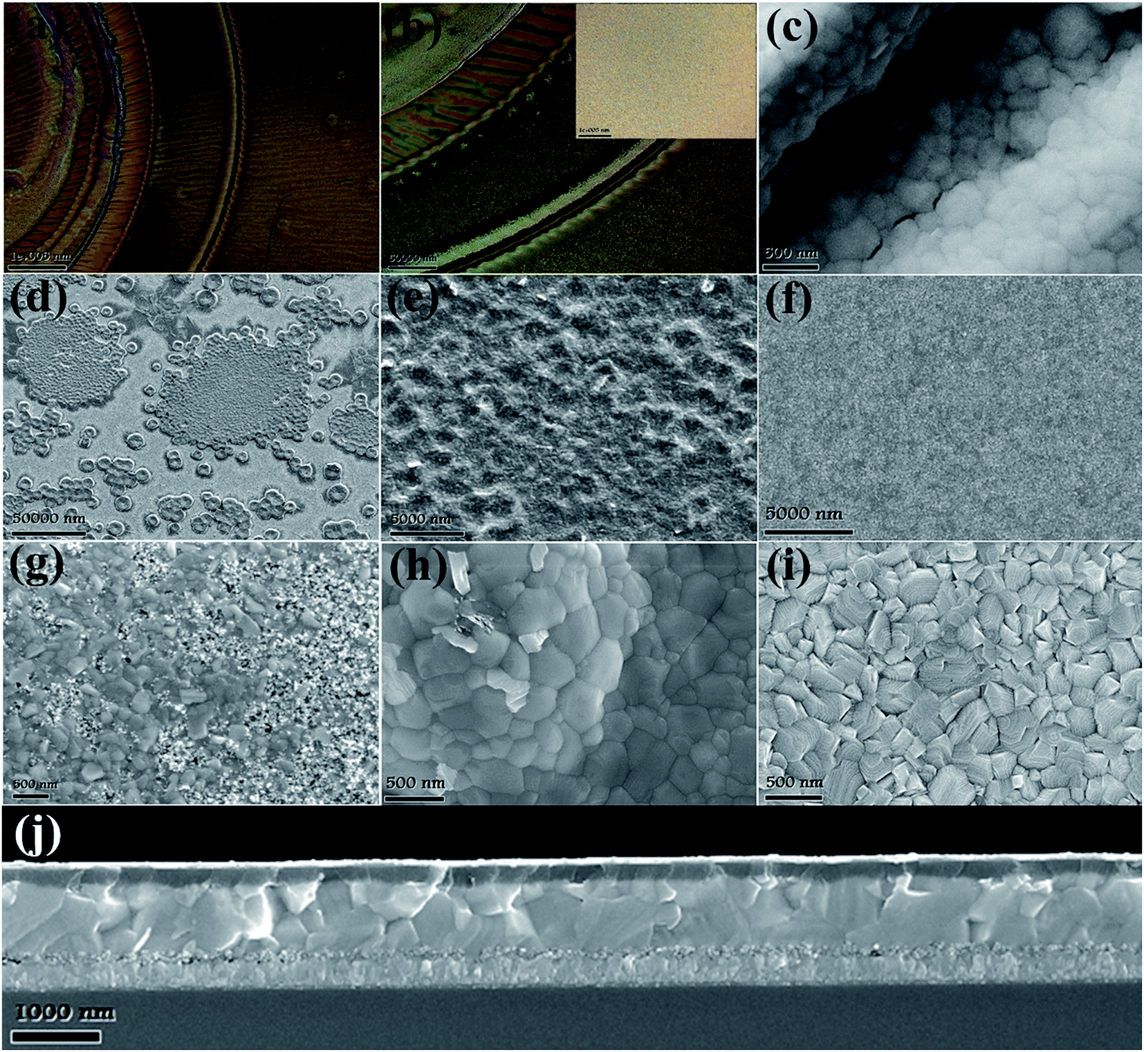 | ||
| Fig. 2 (a, b) Gradually enlarged polarizing microscope images of a damaged film produced by dripping anti-solvent; the film exhibited ring defects. The inset shows a smooth perovskite film surface for contrast. (c) SEM images of the annular raised portion of the ring defects. (d, g) Low magnification and high magnification SEM images of uncovered perovskite film surfaces produced via spraying anti-solvent with spraying operation conditions no. 5 from Table S1.† (e, h) Rough perovskite film surfaces under conditions no. 8 from Table S1.† (f, i) Smooth perovskite film surfaces prepared using optimized operating parameters no. 7 from Table S1.† (j) The SEM cross-sectional images of a high quality device prepared by the SAP method. Grains in film made by SAP are larger than those of the conventional dripping device (Fig. S3†), and the interfaces are smoother. | ||
For further observation, we investigated the morphology of perovskite films by atomic force microscopy (AFM). Perovskite films were prepared on TiO2 coated FTO substrates. AFM images of perovskite film with rings prepared by dripping exhibited a fluctuating surface resembling rippling waves. Countless deep ravines and gullies were distributed throughout the film, which can be observed readily in a three-dimensional image (Fig. S5†). The perovskite films with waves have an increased roughness. The root mean-square of surface roughness (RMS) values of the wave perovskite films and a smooth film with an area of 10 × 10 μm were 18.1 nm and 119.6 nm, respectively. When a film was made by the spraying anti-solvent process under optimal conditions, the film showed better coverage and a more uniform surface than the film with rings. AFM phase images and the corresponding height profile of the cracking films were consistent with SEM.
The crystallinity of the perovskite was increased compared with the conventional dripping method, as shown by the XRD patterns in Fig. 3(a). This result clearly showed that both perovskite films exhibited strong diffraction peaks at 14.1°, 28.4°and 31.9°, which can be indexed to the (110), (220) and (310) planes of the perovskite crystal. The intensity of (110) and (220) peaks were very strong compared to the other peak, demonstrating the better crystallization of perovskite film. Additionally, the XRD spectrum of film made by SAP showed an increase of the diffraction intensity ratio between (110) and (310). This indicated that the orientation of the perovskite crystal was enhanced, which is good for optoelectronic device performance.
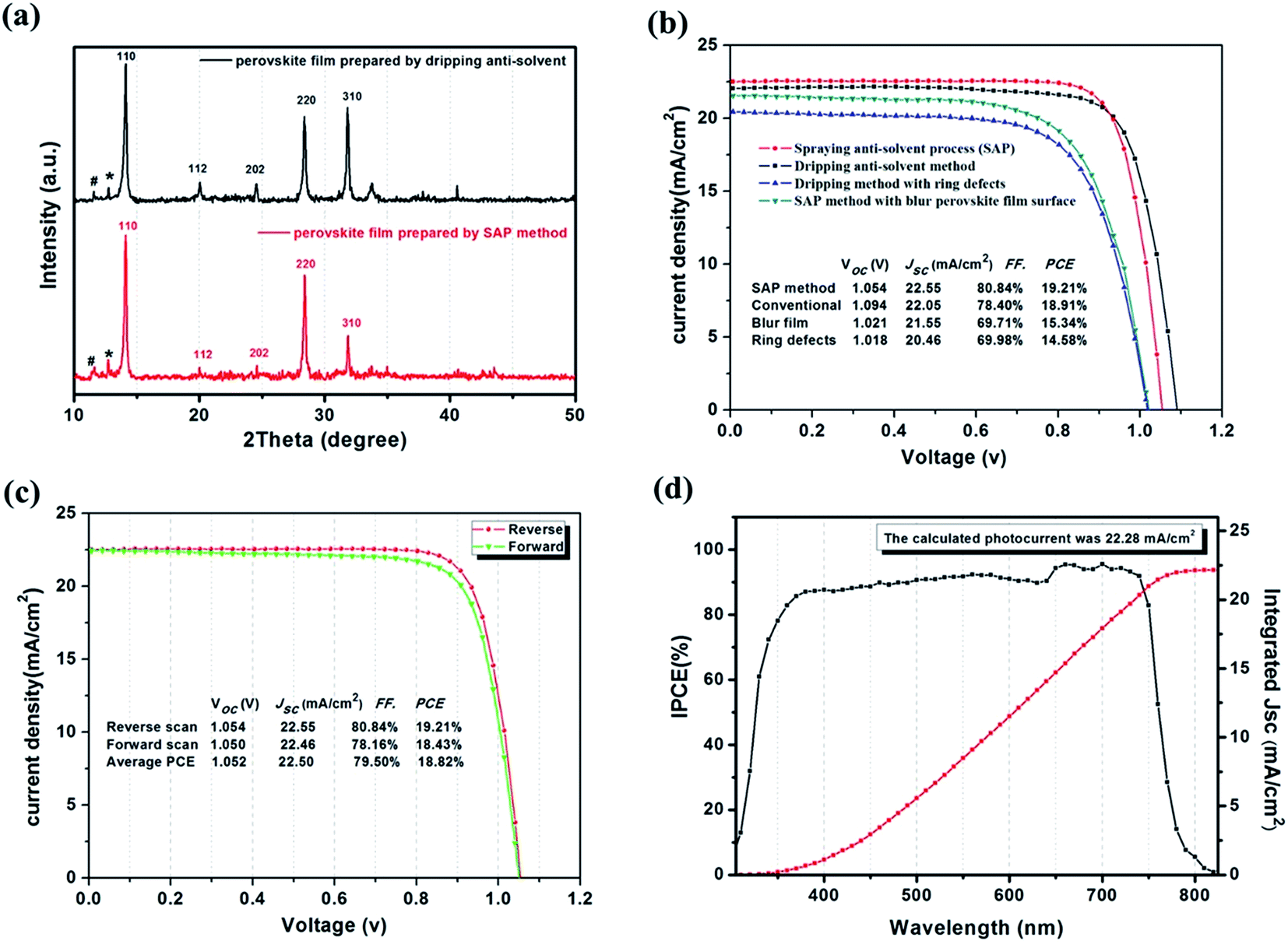 | ||
| Fig. 3 (a) XRD patterns of perovskite films deposited on glass substrates treated by the dripping and SAP method. The PbI2 and yellow phase peak are denoted as * and #, respectively. (b) J–V curves measured at 100 mW cm−2 illumination AM 1.5G. (c) Forward and reverse bias sweep for the best solar cell; the scan speed was 50 mV s−1. (d) Corresponding incident photon-to-current conversion efficiency (IPCE) and integrated Jsc spectra of the device made by the SAP method. | ||
Devices with a structure of FTO/bl-TiO2/meso-TiO2/FA0.81MA0.15Cs0.025PbI2.5Br0.45/HTM/Au were fabricated to investigate the effect of the SAP method on photovoltaic performance. The current density–voltage (J–V) curves of the devices are shown in Fig. 3(b), and the photovoltaic parameters are summarized in the inset Table. The perovskite film with ring defects fabricated by the dripping anti-solvent method leads to an imperfect crystallinity and morphology, resulting in a large leakage current and poor device performance, obtaining only a PCE of 14.58%. In addition, a film without defects showed a Jsc of 22.05 mA cm−2, a Voc of 1.094, a FF of 78.4%, and a total PCE of 18.91%. For comparison, devices fabricated by the SAP method under suitable conditions exhibited an open-circuit voltage (Voc) of 1.054 V, a Jsc of 22.55 mA cm−2, a FF of 80.84% and a PCE of 19.21%. In particular, highly crystalline, more uniform and smoother perovskite films contributed greatly to the increase of the Jsc and FF, giving higher values than previous films. The optimization data for device performance are shown in Fig. 3(c); the device fabricated by SAP gave an average Voc of 1.052 V, a Jsc of 22.50 mA cm−2, a FF of 79.50% and a PCE of 18.82%. The calculated photocurrent from IPCE was 22.28 mA cm−2, which was in close agreement with these measurements. Here the photocurrent hysteresis characteristics for the two types of devices have also been studied; as shown in Fig. S6,† the SAP device had the advantage of suppressing the hysteresis phenomenon. For the conventional device, an obvious change from 18.91% to 16.33% in PCE was found when the voltage scan direction was changed from reverse to forward. In contrast, this photocurrent hysteresis nearly disappeared in the device made by SAP.31 This is consistent with previous studies in which charge traps are one of the origins of photocurrent hysteresis and, consequently, it can be reduced when voids and lots of crystal boundaries are eliminated.
It has been reported that the crystallization and surface structure of perovskite film are related to fluorescence intensity. The steady-state photoluminescence (PL) spectra and dynamics were measured to study the effect of the SAP method on perovskite film quality from perovskite side, and typical sharp PL spectra with very little shift centered at 775 nm were observed in all cases. Fig. 4(a) shows the PL intensity of the corresponding perovskite film; the samples for PL measurement are deposited on a glass substrate. The PL intensity of the film with ring defects decreased obviously compared with the intact film prepared by the dripping method. After SAP, the films exhibited a flatter surface and the PL intensity showed a substantial increase, even higher than a perfect film produced by dripping. This indicated that recombination of charge carriers occurred at a lower speed in the film made by SAP, finally leading to a strong fluorescence signal.
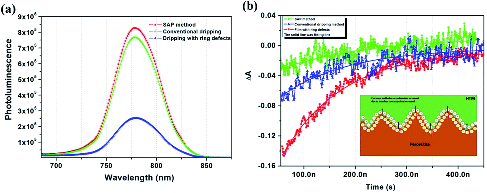 | ||
| Fig. 4 (a) Steady state photoluminescence spectra of two types of perovskite film of glass/perovskite at an excitation wavelength λexc = 490 nm. (b) TAS response of the perovskite film deposited on a glass substrate treated with different methods; the charge carrier lifetime was simulated by LKS (produced by Applied Photophysics). The tests were measured with a pump light wavelength of 500 nm and a probe light wavelength of 775 nm. The red solid line represents the fitting result with single exponential function. The inset is a schematic diagram of charge carrier recombination and a large number of composite sites due to the wave-like defects. | ||
We hypothesized that a low trap density would produce a longer carrier lifetime. To validate our hypothesis, transient absorption spectra (TAS) was measured to detect the electron and hole recombination signal of the perovskite layer to understand further the effect of the method of anti-solvent use on perovskite layer fabrication. TAS were measured from the side of the film which was deposited on the glass. A perovskite layer with a longer lifetime represents a high quality film. Because electrons and holes in a film with cracks and ravines can recombine easily, this is difficult for films with long charge carrier lifetimes. After laser excitation, the electron–hole pairs which are generated in the perovskite films will transit to the conduction band (CB) and the valence band (VB), respectively. There were main three ways for the recombination of charge carriers:32,33 (1) electrons in the CB recombine with holes in the VB directly; (2) electrons recombine with holes due to becoming trapped in structural defects; (3) Auger recombination (there is almost no Auger recombination in our experiment because of the low excition energy). We utilize the single exponential function y = A1exp(−x/τ1) to fit our results, where τ is the time constant and A1 is the contribution from the relevant portions; the fitting results are shown in Fig. 4(b), and the lifetime is shown in Table S2.† We found that there is a main recombination processes, which could be attributed to non-radiative recombination of surface traps or defects and we estimate that the amplitude of the TA signal is proportional to the number of defects.34 By fitting the TA decay, it was found that, with the SAP method, we get a larger τ value of 175.81 ns due to the slow recombination process, which means that there were fewer trap states or defects in the perovskite films. The film prepared by the conventional dripping method exhibited a smaller value of 131.65 ns, which indicated relatively more defects. A decay process appeared in the TA response for the film with ring defects, which showed a value of 118.58 ns, due to serious internal structural defects. Compared with smooth perovskite surface, the wave-like film shows morphological characteristics of high and low fluctuation which produce more defects; as shown in the schematic diagram in the inset of Fig. 4(b). The amount of charge carrier generation was constant, but the recombination sites increased. This will lead to large device current leakage as well as a low FF. In addition, the grain size is relatively small and distributed unevenly, resulting in a clear increase of the grain boundary of the films, so the non-radiative recombination is increased significantly, and the FF and Voc of PSCs are relatively small.
The above results show that method of anti-solvent treatment is important for the formation of perovskite films. For the spray anti-solvent process, we speculate that it could provide a soft impact force and uniform dispersion, which is helpful to improve and optimize the microstructure and film quality. As a result, the charge trap density is dramatically reduced and the grain size becomes larger, which decreases the total grain boundary and is beneficial for device performance.
To check the reproducibility of device performance produced by the anti-solvent spraying method, we repeated the device fabrication using the optimised process. The distributions of the efficiencies are compared using histograms obtained from 24 integrated perovskite devices, as shown in Fig. 5(a) and (b). As can be seen from the results, both of the device-types performed well. The average efficiency of the SAP group (18.14%) was higher than that of the conventional group (17.05%), and the degree of dispersion was smaller. Both of them revealed that reproducibility of the SAP group is improved with respect to the conventional group. Considering that the same TiO2 and HTM layers were used for the two groups of devices, the improved reproducibility of the SAP group should be attributed to the optimized perovskite layer with a mean distribution of crystals.
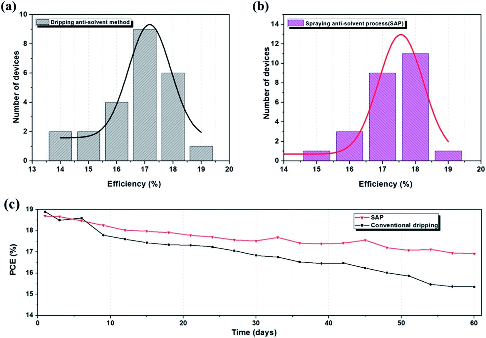 | ||
| Fig. 5 (a, b) Distribution of the efficiencies from the SAP method and the conventional dripping anti-solvent method. (c) Power conversion efficiency as a function of storage time in dry air and dark conditions for the perovskite solar cell with different methods; the test time interval was three days. All devices were tested without any encapsulation. | ||
The high quality of continous perovskite films prepared by the SAP method gives the devices a better photoelectric performance as well as increased stability. The device exhibited a slower deterioration rate with the PCE remaining over 90% when stored in dry air and dark conditions after 60 days. On the contrary, devices made by the dripping anti-solvent method showed a faster deterioration rate with the PCE dropping to 80%, as depicted in Fig. 5(c). The device showed significant superiority probably due to its compact and orderly crystal structure and excellent crystallinity; this will result in the perovskite itself having a strong ability to resist decomposition.
4 Conclusion
In summary, we report a highly reproducible method for controlling perovskite crystal growth by SAP. When the anti-solvent lands on the substrate, the atomized solvent particles are evenly dispersed and contact the film more softly and uniformly, which can reduce waves and eliminate ring-defects of the perovskite film caused by the impact and centrifugal force. By introducing the SAP method, we can control effectively the grain size, surface coverage and flatness of the films. The influence on crystallization, microstructure and carrier transportation properties of the perovskite films were systemically investigated. After optimizing the spraying operating conditions, the power conversion efficiency was boosted from 15.34% to 18.78%. Devices based on the FA0.81MA0.15Cs0.025PbI2.5Br0.45 light absorber showed a record PCE of 19.21% with a high FF of 80.84% measured under conditions of AM 1.5G, 100 mW cm−2, which was equivalent to device made by conventional methods. In addition, this method exhibits good reproducibility and a high FF due to reduced crystal defects in the film. Particularly, the SAP method has great potential possibilities to be applied to large scale manufacturing. It is expected that, by this effective approach, large scale area and high-efficiency PSCs device can be prepared. The application of this approach for large substrate devices is ongoing.Acknowledgements
This work was financially supported by the National High Technology Research and Development Program of China under Grant no. 2015AA050602, the Science and Technology Support program of Jiangsu Province under Grant no. BE2014147-4, and the External Cooperation Program of BIC, Chinese Academy of Sciences (Grant No. GJHZ1607).References
- A. Kojima, K. Teshima, Y. Shirai and T. Miyasaka, J. Am. Chem. Soc., 2009, 131, 6050–6051 CrossRef CAS PubMed.
- M. Liu, M. B. Johnston and H. J. Snaith, Nature, 2013, 501, 395–398 CrossRef CAS PubMed.
- M. M. Lee, J. Teuscher, T. Miyasaka, T. N. Murakami and H. J. Snaith, Science, 2012, 338, 643–647 CrossRef CAS PubMed.
- Q. Dong, Y. Yuan, Y. Shao, Y. Fang, Q. Wang and J. Huang, Energy Environ. Sci., 2015, 8, 2464–2470 CAS.
- J. Burschka, N. Pellet, S. J. Moon, R. Humphry-Baker, P. Gao, M. K. Nazeeruddin and M. Grätzel, Nature, 2013, 499, 316–319 CrossRef CAS PubMed.
- C. W. Chen, H. W. Kang, S. Y. Hsiao, P. F. Yang, K. M. Chiang and H. W. Lin, Adv. Mater., 2014, 26, 6647–6652 CrossRef CAS PubMed.
- K. Cao, Z. Zuo, J. Cui, Y. Shen, T. Moehl, S. M. Zakeeruddin, M. Grätzel and M. Wang, Nano Energy, 2015, 17, 171–179 CrossRef CAS.
- Q. Chen, H. Zhou, Z. Hong, S. Luo, H. S. Duan, H. H. Wang, Y. Liu, G. Li and Y. Yang, J. Am. Chem. Soc., 2014, 136, 622–625 CrossRef CAS PubMed.
- M. Liu, M. B. Johnston and H. J. Snaith, Nature, 2013, 501, 395 CrossRef CAS PubMed.
- S. Wang, L. K. Ono, M. R. Leyden, Y. Kato, S. R. Raga, M. V. Lee and Y. Qi, J. Mater. Chem. A, 2015, 3, 14631–14641 CAS.
- D. E. Swanson, J. M. Kephart, P. S. Kobyakov, K. Walters, K. C. Cameron, K. L. Barth, W. S. Sampath, J. Drayton and J. R. Sites, J. Vac. Sci. Technol., A, 2016, 34, 021202 Search PubMed.
- G. E. Eperon, V. M. Burlakov, P. Docampo, A. Goriely and H. J. Snaith, Adv. Funct. Mater., 2014, 24, 151–157 CrossRef CAS.
- G. Li, T. Zhang and Y. Zhao, J. Mater. Chem. A, 2015, 3, 19674–19678 CAS.
- F. Huang, Y. Dkhissi, W. Huang, M. Xiao, I. Benesperi, S. Rubanov, Y. Zhu, X. Lin, L. Jiang and Y. Zhou, Nano Energy, 2014, 10, 10–18 CrossRef CAS.
- Q. Cao, S. Yang, Q. Gao, L. Lei, Y. Yu, J. Shao and Y. Liu, ACS Appl. Mater. Interfaces, 2016, 8, 7854–7861 CAS.
- F. Li, W. Zhu, C. Bao, T. Yu, Y. Wang, X. Zhou and Z. Zou, Chem. Commun., 2016, 52, 5394–5397 RSC.
- J. Ye, H. Zheng, L. Zhu, X. Zhang, L. Jiang, W. Chen, G. Liu, X. Pan and S. Dai, Sol. Energy Mater. Sol. Cells, 2017, 16060–16066 Search PubMed.
- N. J. Jeon, J. H. Noh, Y. C. Kim, W. S. Yang, S. Ryu and S. I. Seok, Nat. Mater., 2014, 13, 897–903 CrossRef CAS PubMed.
- G. Chen, J. Zheng, L. L. Zheng, X. Yan, H. Lin and F. Zhang, Appl. Surf. Sci., 2017, 392, 960–965 CrossRef CAS.
- G. J. A. H. Wetzelaer, M. Scheepers, A. M. Sempere, C. Momblona, J. Ávila and H. J. Bolink, Adv. Mater., 2015, 27, 1837–1841 CrossRef CAS PubMed.
- Y. Zhao and K. Zhu, J. Phys. Chem. Lett., 2013, 4, 2880–2884 CrossRef CAS.
- Z. Xiao, Q. Dong, C. Bi, Y. Shao, Y. Yuan and J. Huang, Adv. Mater., 2014, 26, 6503–6509 CrossRef CAS PubMed.
- S. Razza, F. D. Giacomo, F. Matteocci, L. Cinà, A. L. Palma, S. Casaluci, P. Cameron, A. D’Epifanio, S. Licoccia and A. Reale, J. Power Sources, 2015, 277, 286–291 CrossRef CAS.
- S. Das, B. Yang, G. Gu, P. C. Joshi, I. N. Ivanov, C. M. Rouleau, T. Aytug, D. B. Geohegan and K. Xiao, ACS Photonics, 2015, 2, 680–686 CrossRef CAS.
- X. Du, Y. Wang, Z. G. Xia and H. Zhou, Appl. Mech. Mater., 2015, 74, 839–843 Search PubMed.
- A. K. Chilvery, P. Guggilla, A. K. Batra, D. D. Gaikwad, J. R. Currie and J. Photon, Energy, 2015, 5, 53–93 Search PubMed.
- F. Li, C. Bao, W. Zhu, B. Lv, W. Tu, Y. U. Tao, J. Yang, X. Zhou, Y. Wang and X. Y. Wang, J. Mater. Chem. A, 2016, 4, 11372–11380 CAS.
- F. Zhang, J. Song, L. Zhang, F. Niu, Y. Hao, P. Zeng, H. Niu, J. Huang and J. Lian, J. Mater. Chem. A, 2016, 4, 8554–8561 CAS.
- H. H. Jin, H. L. Min, H. J. Min and H. I. Sang, J. Mater. Chem. A, 2016, 4, 17636–17642 Search PubMed.
- M. Long, T. Zhang, C. Yang, C. F. Ng, T. C. W. Mak, J. Xu and K. Yan, Nat. Commun., 2016, 7, 13503 CrossRef CAS PubMed.
- A. K. Jena, A. Kulkarni, M. Ikegami and T. Miyasaka, J. Power Sources, 2016, 309, 1–10 CrossRef CAS.
- A. Marchioro, J. Teuscher and D. Friedrich, Nat. Photonics, 2014, 8, 250–255 CrossRef CAS.
- J. A. Christians, J. S. Manser, P. V. Kamat and J. Phys, Chem. Lett., 2015, 6, 2086–2095 CAS.
- S. D. Stranks, G. E. Eperon, G. Grancini, C. Menelaou, M. J. Alcocer, T. Leijtens, L. M. Herz, A. Petrozza and H. J. Snaith, APS Meeting, 2014, pp. 341–344 Search PubMed.
Footnote |
| † Electronic supplementary information (ESI) available. See DOI: 10.1039/c7se00036g |
| This journal is © The Royal Society of Chemistry 2017 |