
 Open Access Article
 This Open Access Article is licensed under a
 Creative Commons Attribution 3.0 Unported Licence
Solution processed single-phase Cu2SnS3 films: structure and photovoltaic performance†
Devendra
Tiwari
a,
Tristan
Koehler
b,
Reiner
Klenk
b and
David J.
Fermin
 *a
*a
aSchool of Chemistry, University of Bristol, Cantocks Close, Bristol BS8 1TS, UK. E-mail: David.Fermin@bristol.ac.uk
bHelmholtz-Zentrum Berlin für Materialien und Energie, Hahn-Meitner-Platz 1, D-14109 Berlin, Germany
First published on 27th March 2017
Abstract
High quality microcrystalline tetragonal p-Cu2SnS3 (CTS) films are prepared by spin-coating a single precursor of metal salts and thiourea on to 5 × 5 cm2 Mo substrates. The best of the solar cells completed on these films with a substrate configuration: glass/Mo/CTS/CdS/i-ZnO/Al:ZnO/Ni–Al and a total area of 0.5 cm2 displays an open-circuit voltage of 206 mV, a fill factor of 34.5%, a short circuit current density of 27.6 mA cm−2 and a power conversion efficiency of 1.9% under simulated AM1.5 illumination. This the best performance reported for such solar architectures obtained by solution processing, with dispersion below 20% for 24 devices. For the first time, the key factors limiting CTS device efficiency are quantitatively established based on temperature dependent current–voltage curves and impedance spectroscopy, namely: (i) carrier recombination at the CTS/CdS interface, (ii) MoS2 non-ohmic back contact, formed due to sulfurization of the top Mo layer, with a barrier height of up to 216 ± 14 meV and (iii) the presence of two trap levels with activation energies 41 ± 0.4 meV and 206 ± 7 meV. The shallower trap is linked Cu vacancies, while the deeper trap is associated with Sn in Cu antisite defects based on DFT supercell calculations.
Introduction
Cu2S absorbers initiated the field of thin film photovoltaics (PVs) with power conversion efficiencies up to 10%, although the cell performance rapidly degraded due to the migration of labile Cu vacancies.1 The field evolved towards chalcopyrite structures with the inclusion of elements such as In and Ga which significantly increase the stability of Cu–S phases.2 Recently, Cu(In,Ga)Se2 solar cells have achieved a record 22.6% efficiency, exceeding those of single-junction Si devices.3 However, In and Ga are rare and expensive elements which can limit the expansion of this technology from gigawatt (GW) to terawatt (TW) installed capacity.4,5 Isoelectronic substitution of In and Ga with earth abundant elements led to the development of materials such as Cu2ZnSn(S,Se)4,6 with devices fabricated via solution processing reaching efficiencies up to 12.6%.7 However, the complexity in the preparation of these materials without elemental disorder, structural defects and compositional inhomogeneity has hindered the process towards improving efficiencies towards the 20% mark.8These studies have reinvigorated research in similar materials from the Cu–Sn–S family. The Cu–Sn–S phase diagram is rich with many stable phases: Cu2SnS3, Cu3SnS4, Cu4SnS4, Cu2Sn3S7, and Cu5Sn2S7; among which only Cu2SnS3 (CTS) has shown photovoltaic potential.9 Theoretically, CTS is shown to have a wide stability range and be devoid of Fermi level pinning, while the other forms exhibit poor hole-mobility, Fermi level pinning or high conductivity.10 Cu2SnS3 has a band gap of approximately 1 eV, an absorption coefficient above 105 cm−1 and conductivity between 0.5 and 10 S cm−1, which correspond to a hole concentration of ∼1018 cm−3 and mobility between 1 and 80 cm2 V−1 s−1.11,12 The present state of the art includes solar cells, featuring materials obtained by physical vapor deposition, with efficiency up to 4.63% for pure CTS and up to 6% for Ge-alloyed CTS.13,14 So far, reports have primarily focused on the material synthesis and assessment of PV properties of CTS and very little knowledge has been gathered with regard to the phenomena limiting the power device conversion.
A variety of physical deposition methods have been employed to prepare CTS including sputtering,11,14–16 thermal or e-beam evaporation,11,13 and pulsed laser deposition.11,17 Wet chemical methods, involving single or sequential steps, have also been implemented such as spin/dip coating,12,18,19,22–25 electrodeposition20,21 and nanoparticle inks.18,19,22 Solution based methods are rather appealing from the manufacturing point of view, particularly in terms of the PV module payback time.7,8,26–29 In the context of CTS based devices, the vast majority of the work has focused on physical vapor deposition, with only two studies employing solution processing generating efficiencies up to 2.1%.23,24
In this contribution, we assessed the PV performance of phase pure CTS films obtained by spin coating a single solution based precursor. The interactions between the metal and sulfur components of the precursor are investigated by IR spectroscopy, while thermally induced crystallization and stability of the CTS phase are probed by thermo-gravimetric analysis and differential scanning calorimetry. X-ray diffraction and Raman spectroscopy confirm the generation of polycrystalline CTS films with a tetragonal phase. Solar cells in the superstrate configuration: glass/Mo/CTS/CdS/i-ZnO/Al:ZnO/Ni–Al were fabricated featuring power conversion efficiencies close to 2%, which in itself is the highest reported for solution processed solar cells in the industrially adopted substrate configuration. Temperature dependent J–V and impedance measurements show that carrier recombination at the CTS/CdS junction is a dominant factor in the cell performance, as well as the presence of two different bulk defect states with activation energies 41 ± 0.4 meV and 206 ± 7 meV. Employing DFT supercell calculations of defect formation energies identifies Sn on Cu antisites as the key bulk recombination state.
Experimental and computational procedure
CTS thin films are processed employing a single solution containing chloride salts of Cu(II) and Sn(II) and thiourea in a dimethyl formamide and isopropanol solvent mixture (1![[thin space (1/6-em)]](https://www.rsc.org/images/entities/char_2009.gif) :1). The solution is spin-coated on to 5 × 5 cm2 Mo coated glass and heated on a hot-plate maintained at 300 °C in air for 2 minutes. This process was repeated 6 times to obtain the desirable film thickness. No blocking layer between Mo and glass is employed in order to minimize Na diffusion from the substrate to the absorber. Finally, the films are annealed in a graphite box with S powder using a MTI-OTF1200X furnace at 550 °C for 30 minutes. Subsequently, the films are etched in 10% KCN (aq.) and then immediately transferred to an aqueous chemical bath for CdS buffer layer deposition, following the methodology described previously for Cu2ZnSnS4 films and devices.30 The bath consists of CdSO4, thiourea and ammonium hydroxide, maintained at 70 °C. Deposition of an i-ZnO and aluminum doped ZnO window layer was performed by sputtering. Finally, a Ni/Al contact grid on top of the solar cell was deposited by evaporation using a shadow mask. Solar cells with an area of 0.5 cm2 are scribed mechanically. No antireflection coating is employed. J–V characteristics of the completed device are measured in the dark and under illumination using an in-house class A solar simulator with a simulated AM 1.5 G spectrum and an integrated power density of 100 mW cm−2 at 23 °C. External quantum efficiency of the cells is attained using dual illumination from halogen and xenon lamps and a Bentham TM 300 monochromator (Bentham instruments). Calibrated Si and Ge photodiodes are used as references for the illumination source in J–V characteristics and quantum efficiency measurements. Low temperature impedance measurements are carried out in the dark using a Solartron Modulab impedance analyzer, interfaced with a Linkam HFS 600PB4 cooling stage, in the frequency range of 0.5 Hz to 1 MHz with no applied DC bias and an AC stimulus of 25 mV.
:1). The solution is spin-coated on to 5 × 5 cm2 Mo coated glass and heated on a hot-plate maintained at 300 °C in air for 2 minutes. This process was repeated 6 times to obtain the desirable film thickness. No blocking layer between Mo and glass is employed in order to minimize Na diffusion from the substrate to the absorber. Finally, the films are annealed in a graphite box with S powder using a MTI-OTF1200X furnace at 550 °C for 30 minutes. Subsequently, the films are etched in 10% KCN (aq.) and then immediately transferred to an aqueous chemical bath for CdS buffer layer deposition, following the methodology described previously for Cu2ZnSnS4 films and devices.30 The bath consists of CdSO4, thiourea and ammonium hydroxide, maintained at 70 °C. Deposition of an i-ZnO and aluminum doped ZnO window layer was performed by sputtering. Finally, a Ni/Al contact grid on top of the solar cell was deposited by evaporation using a shadow mask. Solar cells with an area of 0.5 cm2 are scribed mechanically. No antireflection coating is employed. J–V characteristics of the completed device are measured in the dark and under illumination using an in-house class A solar simulator with a simulated AM 1.5 G spectrum and an integrated power density of 100 mW cm−2 at 23 °C. External quantum efficiency of the cells is attained using dual illumination from halogen and xenon lamps and a Bentham TM 300 monochromator (Bentham instruments). Calibrated Si and Ge photodiodes are used as references for the illumination source in J–V characteristics and quantum efficiency measurements. Low temperature impedance measurements are carried out in the dark using a Solartron Modulab impedance analyzer, interfaced with a Linkam HFS 600PB4 cooling stage, in the frequency range of 0.5 Hz to 1 MHz with no applied DC bias and an AC stimulus of 25 mV.
The enthalpy of formation of different point defects is calculated employing DFT in a 96 atom supercell. Calculations are performed with the CASTEP code employing a DFT pseudopotential approach. A generalized gradient approximation functional: PBESOL with ultrasoft pseudopotentials, an energy cutoff of 500 eV and a Monkhorst–Pack grid with a spacing of ∼0.02 Å is used for geometry optimization and energy calculations. The atomic positions are optimized using a BFGS scheme with convergence tolerances of 1.0 × 10⁻⁷ eV per atom for energy, 0.01 eV Å for maximum force, 0.02 GPa for maximum stress, and 5.0 × 10⁻⁴ Å for maximum displacement.
Results and discussion
CTS films are deposited from a precursor solution containing thiourea as well as Cu(II) and Sn(II) chloride salts dissolved in a dimethyl formamide and 2-propanol solvent mixture. Fig. 1a contrasts the FT-IR spectra of pure thiourea and the precursor solution at room temperature. The key vibrational modes of thiourea undergo a significant change after complexation with metal ions in the precursor. In particular, a red shift of the C![[double bond, length as m-dash]](https://www.rsc.org/images/entities/char_e001.gif) S stretching mode (700–740 cm−1); and a blue shift of N–H stretching modes (3100–3300 cm−1) and coupled modes of C–N stretching and N–H bending (1300–1500 cm−1), are observed. A significant change in the vibrational frequencies of these modes implies a strong interaction between thiourea and metal ions via the S atom. Similar types of complexation have been recently reported in the precursor solution for Cu2ZnSnS4 thin films.30
S stretching mode (700–740 cm−1); and a blue shift of N–H stretching modes (3100–3300 cm−1) and coupled modes of C–N stretching and N–H bending (1300–1500 cm−1), are observed. A significant change in the vibrational frequencies of these modes implies a strong interaction between thiourea and metal ions via the S atom. Similar types of complexation have been recently reported in the precursor solution for Cu2ZnSnS4 thin films.30
 | ||
| Fig. 1 (a) FT-IR spectra of pure thiourea (black) and the precursor (red); (b) X-ray diffraction with Rietveld fitting and (c) Raman spectrum of the CTS film on a Mo substrate. | ||
A Mo coated glass substrate is spin coated with the precursor solution and heated at 300 °C. After the desired thickness is achieved by repeating the last steps, the films are annealed in a S atmosphere at 550 °C. Further details of deposition and processing are provided in the Experimental section. Thermogravimetric analysis of the precursor is shown in Fig. S1,† featuring a weight loss between 180 °C and 320 °C which corresponds to the decomposition of the metal-thiourea precursor to the corresponding sulphide. A small mass loss is also observed between 380 °C and 600 °C, most probably associated with SnS or S. Based on these results, a thermal procedure is established involving a heating step at 300 °C after spin-coating followed by annealing at 550 °C.
Fig. 1b shows a characteristic X-ray diffraction (XRD) pattern of the CTS film on a Mo substrate. CTS has been synthesized in different polymorphs, mostly monoclinic, cubic and tetragonal.15,31–37 Cubic CTS has a zinc blende type of structure. The monoclinic form is essentially a superstructure of the cubic arrangement, while the tetragonal structure derives from the cubic form in case there is a random distribution of Cu and Sn. This canonical relation leads to a similar diffraction pattern for these different CTS phases.37 In order to establish the type of crystal structure, analysis of diffraction patterns employing Rietveld refinement is performed using the Fullprof suite.38 Values of the correlation coefficients Rwp and Rp of 6.48 and 8.26, respectively, indicate a high quality fit. The results suggest that CTS crystallizes in a stannite-like tetragonal polymorph (I![[4 with combining macron]](https://www.rsc.org/images/entities/char_0034_0304.gif) 2m) with lattice parameters a = 5.426(3) Å and b = 10.8375(1) Å.‡
2m) with lattice parameters a = 5.426(3) Å and b = 10.8375(1) Å.‡
A typical Raman spectrum of the CTS thin film is displayed in Fig. 1c. Raman spectroscopy is particularly useful for distinguishing the various polymorphs of CTS, with characteristic bands reported at 290 cm−1 and 352 cm−1 for monoclinic; at 303 cm−1 and 355 cm−1 for cubic and at 336 cm−1 and 351 cm−1 for the tetragonal forms.15,39,40 The spectrum of the thin film shows a broad peak with a shoulder between 300 and 380 cm−1, which can be deconvoluted into two Voigt functions centered at 334 and 352 cm−1. These two modes are consistent with a tetragonal lattice. Based on the XRD and Raman analysis, a schematic of the refined unit cell is shown in Fig. S2.† Each metal site is tetrahedrally coordinated to S atoms and vice versa with absence of a direct S–S bond. The Cu–S distance is estimated to be 2.322 Å while the distances between mixed metal atom sites M(I) and M(II), i.e. Wyckoff positions 4d and 2b, and S are 2.354 Å and 2.364 Å, respectively. The bond angles S–Cu–S, S–M(I)–S and S–M(II)–S vary between −0.62° and +1.16° around the tetrahedral angle. These results are in agreement with previous studies.22,23,32,35 The metal atom distribution on site M(I) is dominated by Cu (56.39% occupancy) while the M(II) site is Sn dominated (52.53% occupancy). The overall unit cell composition reflects a Cu/Sn ratio of 2.12, which is in agreement with the elemental ratio obtained from EDAX.
XPS analysis of the Cu 2p, Sn 3d and S 2p core levels is shown in Fig. 2. The binding energies of Cu 2p3/2 and Cu 2p1/2 are observed to be 933.2 and 953.1 eV, with a full width at half maximum of 1.90 eV and 2.24 eV, respectively, consistent with a Cu+ oxidation state.22,23,32,35 The absence of any satellite or shake-up peak around 942 eV further confirms the absence of the Cu2+ state. In sulfides, the tetragonal coordination of Cu typically promotes the +1 oxidation state, as the Cu d10s1 configuration is the most stable for this geometry. The binding energies of Sn 3d5/2 and 3d3/2 are 486.47 and 494.99 eV, respectively, closely matching those reported for SnS2 (i.e. +4 oxidation state).22,23,32,35 The S 2p3/2 and 2p1/2 are closely located at 161.26 and 162.37 eV, respectively, which is similar to the spectra of CuFeS2. The XPS data allow estimating the relative atomic ratios of Cu/Sn/S of 30.6%/14.7%/50.6%, while the ratios of C and O are 1.5% and 2.6%, respectively. These compositions are consistent with EDX analysis as well as the results from the XRD refinement.
 | ||
| Fig. 2 X-ray photoelectron spectra of the Cu 2p, Sn 3d and S 2p core levels in the CTS films. | ||
The morphology of films as probed through scanning electron microscopy of the CTS film on a Mo coated substrate is presented in Fig. 3a. The films are homogenous and compact with grain sizes between 500 and 1100 nm, which are appropriate for device fabrication. Fig. 3b shows the cross-sectional image of the films which reveals a uniform growth of the adherent film with a thickness of 1.2 μm. The contrast between CTS and the Mo layer indicates the partial sulfurization of the Mo layer at the interface. Formation of this MoS2 would implicate the device performance which will be discussed in the later section. Fig. 3c shows the diffuse reflectance spectrum of the CTS film, featuring a large change in reflectance between 1050 and 1350 nm corresponding to the band-to-band transition. The inset in Fig. 3c corresponds to a modified Tauc's plot using the Kubelka–Munk transformation of the diffuse reflectance, from which an optical band gap of 1.1 eV can be estimated. This value is consistent with previous optical studies of tetragonal CTS.15,23,40
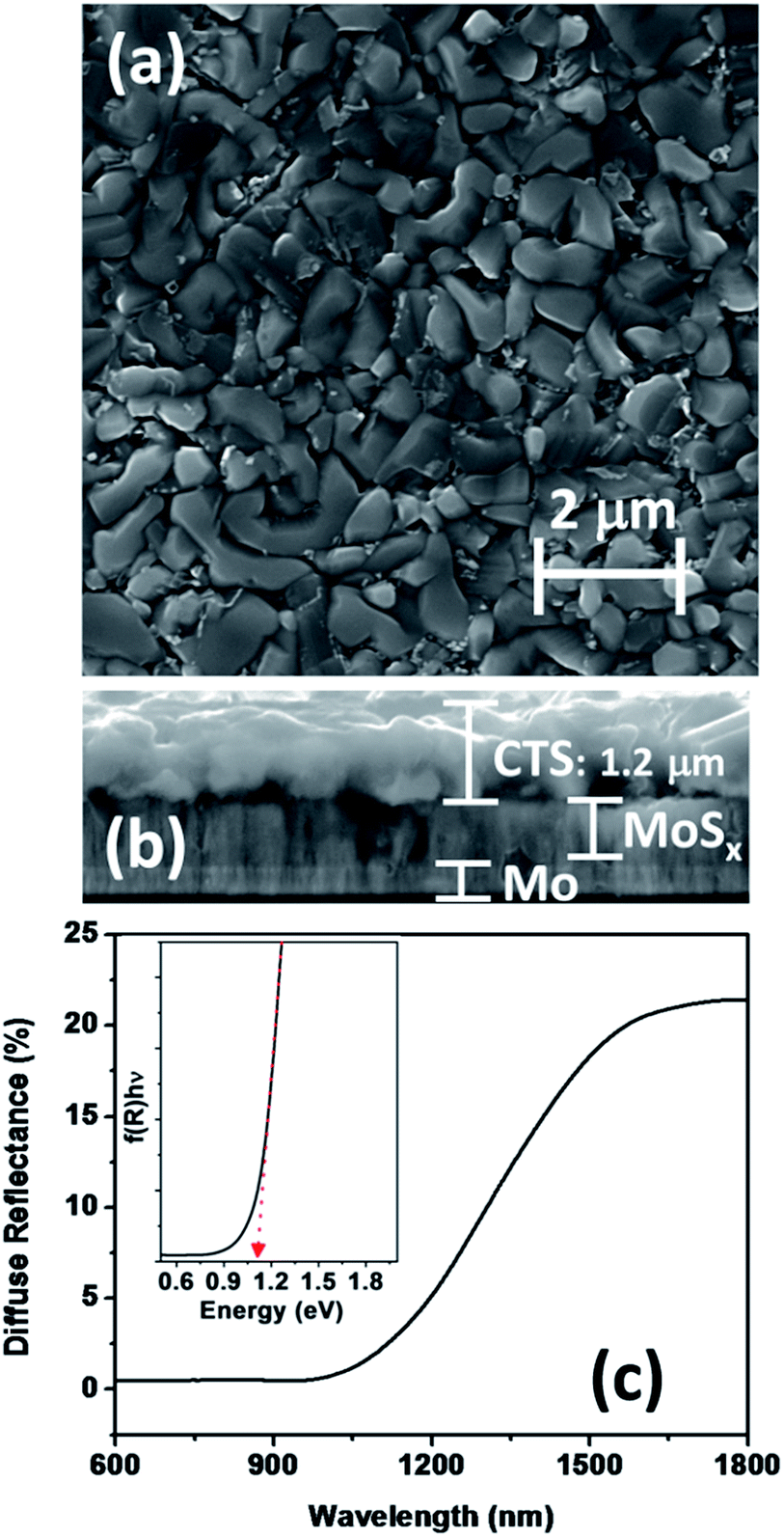 | ||
| Fig. 3 Top (a) and cross-sectional (b) SEM images of a CTS film on a Mo substrate. Diffuse reflectance spectrum of the CTS film, the inset shows a plot for a modified Tauc plot using the Kubelka–Munk transformation of diffuse reflectance to determine the band gap (c). | ||
Four probe conductivity and Hall measurements of the CTS films revealed p-type conductivity with a resistivity and hole mobility of 2.226 Ω cm and 4.581 cm2 V−1 s−1, respectively. These values allow estimating a room temperature hole concentration of 6.12 × 1017 cm−3, which is appropriate for heterojunction solar cell applications. Many of the Cu–Sn–S phases suffer from high carrier concentration limiting their utility for PV devices. Theoretical studies have predicted CTS doping densities between 1015 and 1018 cm−3 due to native vacancies, although other types of defects can contribute as well.10 A combinatorial study of a wide range [Cu]/([Cu] + [Sn]) ratio concluded that values between 0.6 and 0.72 lead to a hole density close to 1018 cm−3.41 This is fully consistent with our findings, considering that the [Cu]/([Cu] + [Sn]) ratio is 0.67.
The performance of 0.5 cm2 devices with the substrate architecture glass/Mo/CTS/CdS/i-ZnO/Al:ZnO/Ni–Al, with no antireflective coating, under a standard simulated AM1.5 spectrum is displayed in Fig. 4. The CdS layer (70 nm) was grown by chemical bath deposition, while the i-ZnO and Al–ZnO layers (400 nm total) were deposited by RF sputtering. The J–V characteristics of the best cell in the dark and under illumination are shown in Fig. 4a, featuring a power conversion efficiency of 1.92%, an open-circuit voltage (VOC) of 206 mV, a fill factor (FF) of 34.5% and a short circuit current density, JSC of 27.6 mA cm−2. These figures of merit are the highest reported for solution processed CTS on a substrate architecture. The relatively narrow dispersion of key parameters for 24 solar cells is summarized in Table S2.†
 | ||
| Fig. 4 Performance of CTS solar cells with the structure: glass/Mo/CIS/CdS/i-ZnO/ZnO:Al/Ni–Al, and a total area of 0.5 cm2: J–V characteristics of the best cell in the dark and under simulated AM1.5 illumination (a); external quantum efficiency spectra of the best device under short-circuit conditions (b); open circuit voltage (VOC), short circuit current (JSC) and power conversion efficiency (η) as a function of temperature (c). Data in (a) and (b) were measured under front illumination at 23 °C. | ||
The spectral response of the best cell is shown in Fig. 4b, showing a maximum external quantum efficiency (EQE) of 70% at around 560 nm. At shorter wavelengths the device performance is restricted by the CdS (540 nm edge) and ZnO layers (400 nm edge). A band gap of 1.1 eV can be estimated from the onset of the EQE spectrum, which corroborates the value estimated from diffuse reflectance (Fig. 3c). The integrated value of the photocurrent over the entire spectrum is found to be 25.8 mA, falling close to the JSC calculated from J–V curves.
Fig. 4c shows the temperature dependence of the key device performance in the range of 300 to 80 K. As the temperature increases, the VOC linearly decreases over large portions of the temperature range, while the JSC slightly increases reaching a maximum at 240 K. The non-monotonic temperature dependence of JSC is a manifestation of a non-linear series resistance, most probably associated with a MoS2 rectifying back contact.42 The device efficiency increases with decreasing temperature reaching a maximum of 4.8% at 120 K. The temperature dependence of the VOC can be expressed in terms of:42–44
 | (1) |
The origin of the interfacial recombination is most likely connected to the cliff like band alignment between CTS and CdS which has been measured using photoelectron spectroscopy.45 Recombination can also be linked to clusters of cation disorder and stacking faults, which has been recently theoretically postulated and experimentally observed employing electron microscopy.46,47 Further studies are required in order to clearly identify the nature of the interfacial recombination site associated with the VOC deficiency shown in Fig. 4c.
As discussed in the ESI,† quantitative analysis of carrier dynamics can be extracted from the temperature dependence of the device impedance spectra (Fig. S3†). A systematic analysis using different equivalent circuits reveals contributions from two RC time constants associated with the CdS/CTS and CTS/MO interfaces, as well as the dynamic responses of two defect sites (Fig. S3a–c†). The adopted equivalent circuit has been used in numerous impedance studies featuring Cu2ZnSnS4, CdTe, CuInSe2 and Cu(In,Ga)Se2 absorbers.42,43,48–50
The temperature dependent relaxation frequency (ωT = 1/RC) of the two defect states measured by impedance spectroscopy is displayed in Fig. 5a, based on the following expression:
 | (2) |
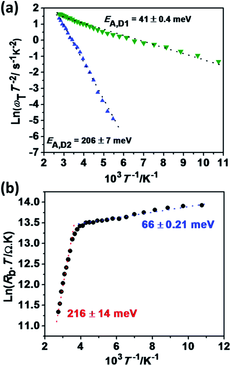 | ||
| Fig. 5 Temperature dependence of the characteristic time constants associated with defect sites obtained from impedance spectroscopy (a). The data are plotted following the Arrhenius formalism (see text). Temperature dependence of the series back resistance (b). Impedance spectra were recorded in the dark between 0.5 Hz and 1 MHz and temperatures ranging from 80 to 370 K. | ||
Both frequencies show a clear Arrhenius behavior over the entire temperature range investigated, providing activation energy values of EA,D1 = 41 ± 0.4 meV and EA,D2 = 206 ± 7 meV. Interestingly, EA,D1 is very similar to the values associated with a Cu vacancy in chalcopyrites and kesterite cells.42,43,48,50 The nature of EA,D2 is discussed further below. The temperature dependence of the back contact Rb is displayed in Fig. 5b. In this case, the temperature dependence can be described in terms of,42–44
 | (3) |
In order to identify the nature of the deep defect state exhibiting an activation barrier of 216 meV, we have performed DFT calculations on a 96 atom monoclinic CTS supercell displayed in Fig. 6a. The use of a monoclinic unit cell as a first approximation can be justified considering that the tetragonal polymorph of CTS is a special case of the cubic form with a random cation distribution, while the cubic form is in itself a superstructure of the monoclinic polymorph.37 Furthermore, the latter is the ground state structure of CTS at 0 K. Calculations on a tetragonal unit cell would require extensive computational resources which are beyond the scope of this work. Details of calculations are included in the Experimental section.
 | ||
| Fig. 6 DFT supercell calculation of point defect formation energies: the 96 atom monoclinic CTS supercell used in calculations (a); simplified schematic of the Cu–Sn–S phase diagram showing the five points at which formation of defects is assessed (b) and formation energies associated with Cu (VCu), Sn (VSn) and S (VS) vacancies as well as Sn on Cu (SnCu) and Cu on Sn (CuSn) antisites at various points on the phase diagram (c). | ||
The formation energies of various types of neutral point defects are calculated at five different points in the Cu–Sn–S ternary phase diagram schematically shown in Fig. 6b. The CTS phase lies at the center of the pentagon, while the five corners represent the points at which CTS is in equilibrium with stable metal, binary or ternary phases. The point defects investigated were Cu (VCu), Sn (VSn), and S (VS) vacancies as well as Cu on Sn (CuSn) and Sn on Cu (SnCu) antisites. The monoclinic structure consists of two different types of Cu sites and three S sites, thus defect formation energies of all of the various sites are calculated.
Fig. 6c shows the formation energies of the various defect sites, revealing that VCu has the lowest formation energy. Consequently, VCu is considered as the main acceptor state of CTS responsible for its p-type conductivity. On the other hand, the key donor state consists of a SnCu defect, exhibiting the second lowest formation energy. VSn and CuSn states appear thermodynamically unfavorable based on these calculations. In view of these findings, the deep state associated with EA,D2 = 206 meV can be attributed to SnCu antisite defects. Interestingly, recent TEM studies with atomic-scale resolution have shown clear evidence of the presence of SnCu antisite domain boundaries in Cu2ZnSnS4 kesterite nanoparticles.51 Consequently, optimization of the CTS preparation is required in order to simultaneously control the doping density via VCu and suppress the SnCu bulk recombination sites. Solution based precursor methods as described in this work are uniquely suited to explore these conditions by: (i) controlling the composition ratio of the elemental precursors and (ii) introduction of dopants which can decrease atomic disorder.30
Conclusions
The present report unveils the key factors limiting the efficiency of thin-film PV devices featuring phase pure polycrystalline CTS films. We describe a new methodology for preparing high quality CTS films featuring a tetragonal structure and metal poor composition. The film exhibits a band gap of 1.1 eV (direct transition) as well as micron scale grain sizes which are ideal for PV applications. The best solar cell device features a power conversion efficiency of 1.9%, with a VOC of 200 mV, fill factor of 34.5% and JSC of 27.6 mA cm−2. These figures of merit are amongst the highest reported for CTS devices. Temperature dependent J–V and electrical impedance measurements were carried out in order to assess the key parameters limiting the efficiency of the devices. Extrapolating the VOC to 0 K provides a value of 610 mV, which is significantly lower than 1.1 V as expected from the band gap. This behavior points towards interfacial recombination losses at the CTS/CdS interface, which is most probably connected to the misalignment of the band edge energies. The generation of a MoS2 layer at the back contact during the film formation also generates an electronic barrier with an activation energy as high as 206 meV, while impedance spectroscopy allowed estimating two characteristic frequencies associated with defect states. The shallower one features an activation energy of approximately 40 meV, which is consistent with states generated by Cu vacancies as seen in related materials such as CuInSe2 and Cu2ZnSnS4. DFT supercell calculations of the formation energies of different defects suggest that the deeper state with an activation energy just over 200 meV corresponds to a SnCu antisite. In addition to investigating alternative absorber layers that can offer a more appropriate band alignment, our work shows that manipulating the composition of the molecular precursor solution and/or adjusting the annealing conditions in order to minimize structural disorder can generate significant improvement in cell efficiencies.Acknowledgements
DT and DJF are grateful to the funding by the UK Engineering and Physical Sciences Research Council (EPSRC) via the PVTEAM Program (EP/L017792/1). DJF acknowledges the support by the Institute of Advanced Studies of the University of Bristol, (University Research Fellowship 2015). Microscopy analysis was performed at the Chemical Imaging Facility, University of Bristol, with equipment funded by EPSRC Grant “Atoms to Applications” (EP/K035746/1). The Solartron Modulab impedance analyzer used in this study was purchased under the EPSRC CDT Capital grant EP/K035746/1. The authors are also indebted to the support from the Helmholtz Zentrum für Materialien und Energie Berlin. The DFT calculations were carried out using the computational facilities of the Advanced Computing Research Centre, University of Bristol – http://www.bris.ac.uk/acrc/.Notes and references
- S. Martinuzzi, Sol. Cells, 1982, 5, 243–268 CrossRef CAS.
- B. J. Stanbery, Crit. Rev. Solid State Mater. Sci., 2002, 27, 73–117 CrossRef CAS.
- P. Jackson, R. Wuerz, D. Hariskos, E. Lotter, W. Witte and M. Powalla, Phys. Status Solidi RRL, 2016, 10, 583–586 CrossRef CAS.
- Report on the critical raw materials for the European commission, 2014, p. 41 Search PubMed.
- Critical Materials Strategy, US Department of Energy, 2012, DOE/PI-000, pp. 1–29 Search PubMed.
- I. Repins, N. Vora, C. Beall, S.-H. Wei, Y. Yan, M. Romero, G. Teeter, H. Du, B. To, M. Young and R. Noufi, MRS Online Proc. Libr., 2011, 1324, d17 Search PubMed.
- W. Wang, M. T. Winkler, O. Gunawan, T. Gokmen, T. K. Todorov, Y. Zhu and D. B. Mitzi, Adv. Energy Mater., 2014, 4, 1301465 CrossRef.
- X. Liu, Y. Feng, H. Cui, F. Liu, X. Hao, G. Conibeer, D. B. Mitzi and M. Green, Prog. Photovoltaics Res. Appl., 2016, 24, 879 CrossRef.
- S. Fiechter, M. Martinez, G. Schmidt, W. Henrion and Y. Tomm, J. Phys. Chem. Solids, 2003, 64, 1859–1862 CrossRef CAS.
- P. Zawadzki, L. L. Baranowski, H. Peng, E. S. Toberer, D. S. Ginley, W. Tumas, A. Zakutayev and S. Lany, Appl. Phys. Lett., 2013, 103, 253902 CrossRef.
- A. C. Lokhande, R. B. V. Chalapathy, M. He, E. Jo, M. Gang, S. A. Pawar, C. D. Lokhande and J. H. Kim, Sol. Energy Mater. Sol. Cells, 2016, 153, 84–107 CrossRef CAS.
- D. Tiwari, T. K. Chaudhuri and T. Shripathi, Appl. Surf. Sci., 2014, 297, 158–166 CrossRef CAS.
- M. Nakashima and M. Izaki, Appl. Phys. Express, 2015, 42303, 42303 CrossRef.
- M. Umehara, Y. Takeda, T. Motohiro, T. Sakai, H. Awano and R. Maekawa, Appl. Phys. Express, 2013, 6, 45501 CrossRef.
- P. A. Fernandes, P. M. P. Salome and A. F. Da Cunha, Phys. Status Solidi C, 2010, 7, 901–904 CAS.
- R. Chierchia, F. Pigna, M. Valentini, C. Malerba, E. Salza, P. Mangiapane, T. Polichetti and A. Mittiga, Phys. Status Solidi C, 2016, 13, 35–39 CrossRef CAS.
- S. A. Vanalakar, G. L. Agawane, A. S. Kamble, C. W. Hong, P. S. Patil and J. H. Kim, Sol. Energy Mater. Sol. Cells, 2015, 138, 1–8 CrossRef CAS.
- S. A. Vanalakar, G. L. Agawane, S. W. Shin, H. S. Yang, P. S. Patil, J. Y. Kim and J. H. Kim, Acta Mater., 2015, 85, 314–321 CrossRef CAS.
- A. C. Lokhande, K. V. Gurav, E. Jo, C. D. Lokhande and J. H. Kim, J. Alloys Compd., 2016, 656, 295–310 CrossRef CAS.
- J. Koike, K. Chino, N. Aihara, H. Araki, R. Nakamura, K. Jimbo and H. Katagiri, Jpn. J. Appl. Phys., 2012, 51, 10NC34 CrossRef.
- D. M. Berg, R. Djemour, L. Gütay, G. Zoppi, S. Siebentritt and P. J. Dale, Thin Solid Films, 2012, 520, 6291–6294 CrossRef CAS.
- D. Tiwari, T. K. Chaudhuri, T. Shripathi, U. Deshpande and V. G. Sathe, Appl. Phys. A: Mater. Sci. Process., 2014, 117, 1139–1146 CrossRef CAS.
- D. Tiwari, T. K. Chaudhuri, T. Shripathi, U. Deshpande and R. Rawat, Sol. Energy Mater. Sol. Cells, 2013, 113, 165–170 CrossRef CAS.
- J. Li, J. Huang, Y. Zhang, Y. Wang, C. Xue, G. Jiang, W. Liu and C. Zhu, RSC Adv., 2016, 6, 58786–58795 RSC.
- H. Dahman and L. El Mir, J. Mater. Sci.: Mater. Electron., 2015, 26, 6032–6039 CrossRef CAS.
- T. Todorov and D. B. Mitzi, Eur. J. Inorg. Chem., 2010, 1, 17–28 CrossRef.
- H. Azimi, Y. Hou and C. J. Brabec, Energy Environ. Sci., 2014, 7, 1829–1849 CAS.
- Y. E. Romanyuk, H. Hagendorfer, P. Stücheli, P. Fuchs, A. R. Uhl, C. M. Sutter-Fella, M. Werner, S. Haass, J. Stückelberger, C. Broussillou, P. P. Grand, V. Bermudez and A. N. Tiwari, Adv. Funct. Mater., 2015, 25, 12–27 CrossRef CAS.
- C. J. Hibberd, E. Chassaing, W. Liu, D. B. Mitzi, D. Lincot and A. N. Tiwari, Prog. Photovoltaics Res. Appl., 2010, 18, 434–452 CrossRef CAS.
- D. Tiwari, T. Koehler, X. Lin, R. Harniman, I. Griffiths, L. Wang, D. Cherns, R. Klenk and D. J. Fermin, Chem. Mater., 2016, 28, 4991–4997 CrossRef CAS.
- G. S. Babu, Y. B. K. Kumar, Y. B. K. Reddy and V. S. Raja, Mater. Chem. Phys., 2006, 96, 442–446 CrossRef CAS.
- X. Chen, H. Wada, A. Sato and M. Mieno, J. Solid State Chem., 1998, 139, 144–151 CrossRef CAS.
- G. E. Delgado, A. J. Mora, G. Marcano and C. Rincón, Mater. Res. Bull., 2003, 38, 1949–1955 CrossRef CAS.
- M. Onoda, X. A. Chen, A. Sato and H. Wada, Mater. Res. Bull., 2000, 35, 1563–1570 CrossRef CAS.
- D. Tiwari, T. K. Chaudhuri, T. Shripathi and U. Deshpande, J. Phys. Chem. Solids, 2014, 75, 410–415 CrossRef CAS.
- C. Wu, Z. Hu, C. Wang, H. Sheng, J. Yang and Y. Xie, Appl. Phys. Lett., 2007, 91, 143104 CrossRef.
- Y. T. Zhai, S. Chen, J. H. Yang, H. J. Xiang, X. G. Gong, A. Walsh, J. Kang and S. H. Wei, Phys. Rev. B: Condens. Matter Mater. Phys., 2011, 84, 75213 CrossRef.
- J. Rodríguez-Carvajal, Phys. B, 1993, 192, 55–69 CrossRef.
- D. M. Berg, R. Djemour, L. Gütay, S. Siebentritt, P. J. Dale, X. Fontane, V. Izquierdo-Roca and A. Pérez-Rodriguez, Appl. Phys. Lett., 2012, 100, 192103 CrossRef.
- D. Tiwari, T. K. Chaudhuri, T. Shripathi, U. Deshpande and V. G. Sathe, J. Mater. Sci.: Mater. Electron., 2014, 25, 3687–3694 CrossRef CAS.
- L. L. Baranowski, P. Zawadzki, S. Christensen, D. Nordlund, S. Lany, A. C. Tamboli, L. Gedvilas, D. S. Ginley, W. Tumas, E. S. Toberer and A. Zakutayev, Chem. Mater., 2014, 26, 4951–4959 CrossRef CAS.
- U. Rau, A.-R. Daniel and T. Kirchartz, Advanced Characterization Techniques for Thin Film Solar Cells, Weinheim, Germany, 2011 Search PubMed.
- P. A. Fernandes, A. F. Sartori, P. M. P. Salome, J. Malaquias, A. F. Da Cunha, M. P. F. Gracia and J. C. Gonzalez, Appl. Phys. Lett., 2012, 100, 233504 CrossRef.
- D. Tiwari, D. J. Fermin, T. K. Chaudhuri and A. Ray, J. Phys. Chem. C, 2015, 119, 5872–5877 CAS.
- S. Sato, H. Sumi, G. Shi and M. Sugiyama, Phys. Status Solidi C, 2015, 12, 757–760 CrossRef CAS.
- L. L. Baranowski, K. McLaughlin, P. Zawadzki, S. Lany, A. Norman, H. Hempel, R. Eichberger, T. Unold, E. S. Toberer and A. Zakutayev, Phys. Rev. Appl., 2015, 4, 44017 CrossRef.
- P. Zawadzki, A. Zakutayev and S. Lany, Phys. Rev. Appl., 2015, 3, 34007 CrossRef.
- J. Krustok, M. Danilson, A. Jagomägi, M. Grossberg and J. Raudoja, Proc. SPIE, 2006, 5946, 59460w Search PubMed.
- Y. Y. Proskuryakov, K. Durose, B. M. Taele and S. Oelting, J. Appl. Phys., 2007, 102, 24504 CrossRef.
- T. Walter, R. Herberholz, C. Müller and H. W. Schock, J. Appl. Phys., 1996, 80, 4411–4420 CrossRef CAS.
- N. Kattan, I. Griffiths, D. Cherns and D. J. Fermin, Nanoscale, 2016, 8, 14369–14373 RSC.
Footnotes |
| † Electronic supplementary information (ESI) available: This includes film characterization details, thermogravimetric analysis of the precursor, schematic of the refined crystal structure, typical impedance spectra of devices with trial circuits and temperature dependence of R1, C1, R2 and C2. See DOI: 10.1039/c7se00150a |
| ‡ Further details of the crystal structure investigation(s) may be obtained from the Fachinformationszentrum Karlsruhe, 76344 Eggenstein-Leopoldshafen (Germany), on quoting the depository number CSD-432354. |
| This journal is © The Royal Society of Chemistry 2017 |