
 Open Access Article
 This Open Access Article is licensed under a Creative Commons Attribution-Non Commercial 3.0 Unported Licence
Thickness dependence of structure and superconductivity of the SmBa2Cu3O7 film by laser CVD
Ting Wanga,
Kaidong Wanga,
Rong Tu *a,
Song Zhanga,
Meijun Yanga,
Qizhong Lib,
Ji Shiac,
Haiwen Liad,
Takashi Gotoae and
Lianmeng Zhanga
*a,
Song Zhanga,
Meijun Yanga,
Qizhong Lib,
Ji Shiac,
Haiwen Liad,
Takashi Gotoae and
Lianmeng Zhanga
aState Key Laboratory of Advanced Technology for Materials Synthesis and Processing, Wuhan University of Technology, Wuhan 430070, P. R. China. E-mail: turong@whut.edu.cn
bHubei Key Laboratory of Advanced Technology for Automotive Components, Wuhan University of Technology, Wuhan 430070, P. R. China
cSchool of Materials and Chemical Technology, Tokyo Institute of Technology, Tokyo 152-8552, Japan
dInternational Research Center for Hydrogen Energy, Kyushu University, Fukuoka 819-0395, Japan
eInstitute for Materials Research, Tohoku University, Sendai 980-8577, Japan
First published on 12th December 2017
Abstract
SmBa2Cu3O7 (SmBCO) superconductive films with thicknesses in the range from 0.47 to 2.72 μm were prepared on single-crystalline LAO (100) substrates by laser chemical vapor deposition (laser CVD). The effect of thickness on the orientation, microstructure, and superconductivity of SmBCO films was investigated. The preferred orientation of the SmBCO film changed from c-axis to a- and c-axis co-orientation with an increase in thickness from 0.47 to 2.72 μm. The SmBCO film with 1.06 μm thickness exhibited excellent c-axis epitaxial orientation with a minimum full width at half maximum of 1.07° for φ-scan and an in-plane epitaxial orientation relationship of SmBCO[100]//LAO[010] and SmBCO[010]//LAO[001]. The highest critical transition temperature and critical current density were 89.5 K and 1.92 MA cm−2 (corresponding to the critical current of 204 A cm−1-W) with a deposition rate of 7.6 μm h−1.
1. Introduction
The high-temperature superconductor SmBa2Cu3O7 (SmBCO) with a high critical temperature (TC) and critical current density (JC)1,2 has many application prospects such as high-field magnets, power generators, and electric power distribution systems.3,4 To realize industrial applications, the SmBCO film must have higher critical current (IC) at liquid nitrogen temperature. Thus, one of the effective methods to improve the IC of the SmBCO films is to increase the thickness of the films.5–7 However, the increment of IC tends to slow down with the thickening of the film because a-axis oriented grains and other rotated grains are formed easily in thick films.8 The random-oriented grains would obstruct the current transmission and further result in the saturation of IC because the current is known to travel on the CuO2-plane that parallels to the ab-plane in the c-axis-oriented SmBCO film.8,9 In addition, some Ba–Cu–O and Cu–O impurities are easily formed in the thick films, which have enormous negative influence on the superconductive properties of the film.10,11 The critical current density (JC) decreases sharply with an increase in a-axis oriented grains and impurity grains.8,12 The formation of these unexpected grains is always caused by supersaturation and nonstoichiometric precursor vapor in the later stage of film deposition.13 Therefore, it is of great significance to investigate the effect of thickness on the microstructure and superconductivity of the SmBCO film.Organometallic chemical vapor deposition (MOCVD) is a promising technique for depositing a high crystallinity film because of its high deposition rate, low vacuum requirement, and controllability of the preferred orientation.14–16 However, in the traditional MOCVD setup, since the substrate is usually heated at the bottom, the deposition temperature generally decreases as the thickness of the film increases during the MOCVD process; this may lead to the generation of a-axis grains.17 Moreover, the deposition rate of the SmBCO film deposited by MOCVD is only 0.1–1.5 μm h−1,12,17,18 which limits the industrial application of this film. Therefore, we introduced a laser beam with a large spot size into CVD to heat the top surface of the film and enhance the deposition rate by activating precursor vapors.19–21 Zhao et al.22 adopted laser CVD to prepare a c-axis-oriented YBa2Cu3O7 (YBCO) film on MgO at a high deposition rate of 57 μm h−1. Hence, laser CVD could be a promising process to prepare a thick c-axis-oriented SmBCO superconductive film at a high deposition rate.
In the present study, we deposited SmBCO films on LAO substrates at different deposition time to obtain different thicknesses by laser CVD. The effect of the thickness of film on orientation, microstructure, and critical temperature of the SmBCO films was investigated.
2. Experimental
SmBCO films were prepared on single-crystalline (100)-LaAlO3 (LAO) (10 × 5 × 0.5 mm) substrates by laser CVD. A continuous wave semiconductor laser (wavelength: 808 nm) was adopted in the home-made vertical cold-wall laser CVD apparatus to heat the substrate. The precursors Sm(dpm)3, Ba(dpm)2, and Cu(dpm)2 (Toshima Manufacturing Co. Ltd., Japan) were vaporized in independent vessels at the vaporizing temperatures of 190, 300, and 168 °C, respectively. The vapors were transported into the chamber by Ar gas (≥99.999%) at the flow rate of 100 sccm. O2 (≥99.995%) as the reactant gas was introduced directly into the chamber at the flow rate of 300 sccm. To prevent the precursor vapors from condensing, gas pipelines and nozzles were heated at 350 and 380 °C, respectively. The total pressure (Ptot) of the chamber was fixed at 600 Pa. The substrates were preheated at the laser power (PL) of 55 W with a beam diameter of 15 mm. The SmBCO film was deposited for 240–1200 s to obtain different thicknesses. After deposition, the SmBCO films were heat-treated at PL = 22 W for 1 h in pure O2 under atmospheric pressure.The crystalline phase and in-plane orientation (pole figure) of the SmBCO films were measured by X-ray diffraction (XRD; Ultima-III, 40 kV and 40 mA, Rigaku, Japan) with Cu-Kα radiation (wavelength, 0.15406 nm). The schematic of the crystal growth relationship was drawn by the VESTA software. The Lotgering factor was used to evaluate the degree of the preferred orientation (f) of the SmBCO film:23

The surface and cross-sectional morphology were characterized by field emission scanning electron microscopy (FESEM; FEI Quanta-250, 20 kV, USA). The energy dispersive spectroscopy (EDS) attached to the FESEM was applied to measure the composition of the SmBCO film. Transmission electron microscopy (TEM; JEOL JEM-2100, 200 kV, Tokyo, Japan) was used to observe the cross-sectional nanostructure of the SmBCO film. The superconducting transition temperatures (TC) for the SmBCO films were measured with a standard four-point-probe using a physical property measurement system (PPMS9, Quantum Design, USA) in the range of 10–300 K. The critical current (IC) and critical current density (JC) were measured at 77 K and self-field with a voltage criterion of 1 μV cm−1.24
3. Results and discussion
To study the thickness dependence of the structure and superconducting properties of SmBCO films, a series of samples with different thicknesses were deposited on LAO (100) substrates by controlling the deposition time. From Fig. 1(a), it can be seen that the film thickness (d) closely fits on a line for the growth time; this implies that the laser CVD technique has good controllability on the film thickness. The average deposition rate (Rdep) of the SmBCO films was 7.6 μm h−1. Fig. 1(b) shows the comparison of Rdep of the SmBCO and YBCO films deposited by MOCVD and laser CVD. The Rdep of the films deposited by laser CVD in our study was much higher than of those deposited by MOCVD.12,17,25–28 In laser CVD, the laser irradiation caused thermal decomposition and activated chemical reaction of the precursor in the gas phase and/or substrate surface; thereby, the Rdep was improved significantly, and the deposition temperature was lower than that in the traditional CVD. In the thermal CVD processes, the gas precursors may not get enough energy from the substrate to have fast chemical reactions; thus, the Rdep of the film is degraded.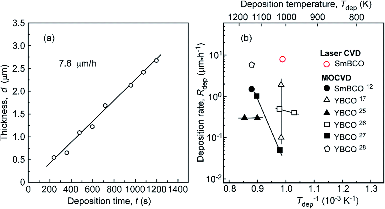 | ||
| Fig. 1 (a) Thickness of the SmBCO film as a function of deposition time and (b) deposition rate (Rdep) of the films prepared by laser CVD and MOCVD. | ||
Fig. 2 exhibits the XRD patterns of SmBCO films with varied thicknesses (d). The SmBCO film with d = 0.47 μm showed weak (00l) diffraction peaks (Fig. 2(a)). As the thickness increased to 1.06 μm, the intensity of the (00l) diffraction peaks was obviously enhanced, and no other peak was observed (Fig. 1(b)). In Fig. 2(c), the film with d = 1.71 μm generated small (h00) diffraction peaks. When the thickness of the SmBCO film increased to 2.72 μm (Fig. 2(d)), the intensity of the (h00) peaks was significantly increased and stronger than that of the (00l) peaks; this indicated considerable concentration of the a-axis-oriented SmBCO grains in the film. Moreover, the BaCuO2 phase was observed in the SmBCO films with 1.71–2.72 μm thickness (Fig. 2(c) and (d)). The appearance of a-axis oriented grains and BaCuO2 grains would cause negative effects on the superconductivity of the SmBCO film.12,13
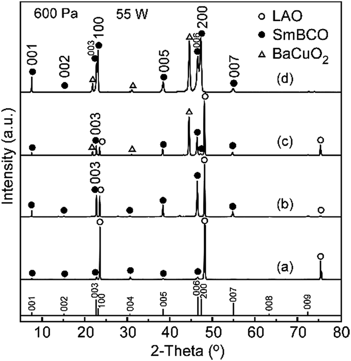 | ||
| Fig. 2 XRD patterns of the SmBCO films prepared on the LAO substrate with the thickness of (a) 0.47, (b) 1.06, (c) 1.71, and (d) 2.72 μm. | ||
Fig. 3 shows the effect of thickness on the preferred orientation degree (f) of the a-axis and c-axis-oriented SmBCO film. The Lotgering factor of c-axis orientation (fc-axis) was almost 1 when the thickness was less than 1.06 μm, indicating fully c-axis-oriented SmBCO films. With an increase in the thickness of the SmBCO film from 1.22 to 2.49 μm, the fc-axis decreased, whereas fa-axis increased; this implied the increase of a-axis-oriented grains. The fc-axis and fa-axis kept constant at 0.43 and 0.46 with a further increase in the thickness, respectively. Thus, the SmBCO film gradually transformed from the fully c-axis orientation to the partially a-axis as the thickness increased. This trend was similar to that of the YBCO deposited by laser CVD.7 The thickness of the pure c-axis-oriented SmBCO film was higher than that reported in literature, e.g., 0.46![[thin space (1/6-em)]](https://www.rsc.org/images/entities/char_2009.gif) 7 and 0.3 μm.29
7 and 0.3 μm.29
 | ||
| Fig. 3 Preferred orientation of the SmBCO films as a function of thickness. | ||
Fig. 4(a) shows the X-ray pole figure pattern generated from the (116) reflection of the SmBCO film with d = 1.06 μm and that of the (111) reflection from the LAO substrate. The SmBCO (116) reflection exhibited four poles at an elevation angle (χ) around 54°. The elevation angle was attributed to the SmBCO (116) plane with a tilt angle of 54° from the SmBCO (001) plane normal direction. Furthermore, the four poles located at the same χ; this indicated that the pure c-axis-oriented SmBCO epitaxial film was obtained, which was consistent with the result of θ–2θ reflection in Fig. 2(b). The epitaxial relationship of the c-axis-oriented SmBCO film and LAO (100) substrate is depicted in Fig. 4(b). The azimuth angles (φ) of the four poles of SmBCO (116) reflection were the same as those of LAO (111) reflection; this indicated the epitaxial relationship of SmBCO[100]//LAO[010] and SmBCO[010]//LAO[001] for the c-axis-oriented SmBCO grains.
 | ||
| Fig. 4 XRD pole figures of (116) reflection of SmBCO films with d = (a) 1.06 and (c) 2.72 μm as well as (111) reflection of the corresponding LAO substrates. In-plane epitaxial growth relationship of the (b) c-axis oriented, and that of the (d) a- and c-axis co-oriented SmBCO films. | ||
The X-ray pole figure of the SmBCO film with d = 2.72 μm shows four poles at χ = 54° and eight poles at χ = 24° in Fig. 4(c). The four poles in the elevation angle of 54° were attributed to the c-axis-oriented SmBCO grains. The {116} reflection at χ = 24° possessed two sets of four fold poles with each of them located at an azimuth angle of 58° or 122° apart from its two adjacent poles. The elevation angle (χ = 24°) was the tilt angle of the (116) plane from the (100) plane normal direction. Furthermore, the SmBCO {116} planes appeared twice with a repeating angle of 90°; this was ascribed to a 90° twinning structure of the a-axis-oriented grains. The azimuth angles (φ) from each pole of the SmBCO {116} planes to its nearest pole of the LAO (111) plane were determined to be 18°. This result coincided with the calculated azimuth angle between the pole of the LAO (111) plane in the [100] projection and that of the SmBCO (116) plane in the [100] projection. Therefore, b- and c-axis of a-axis-oriented SmBCO grains were aligned with those of the substrate. Accordingly, the epitaxial relationship of a- and c-axis co-oriented SmBCO films and LAO substrate is displayed in Fig. 4(d), where the 90° twinning relationship is also presented.30
Fig. 5 shows the comparison of FWHM of SmBCO and YBCO films with different deposition methods. For the SmBCO film deposited by laser CVD in our study, the FWHM of φ-scan decreased from 1.62° to 1.07° with an increase in thickness from 0.47 to 1.06 μm and then increased to 1.89° with a further increase in thickness. The minimum of the FWHM of φ-scan was 1.07° at d = 1.06 μm, indicating that the film had a fine crystallinity. The SmBCO film thicker than 1.71 μm had a- and c-axis co-orientation. The formation of a-axis grains destroyed the film crystallinity structure and further weakened the superconductive property of the SmBCO film.8,9 The films deposited by laser CVD had higher crystallinity and in-plane orientation than those deposited by other methods.31,32 The chemical reactions of film can be activated by intense laser irradiation, which resulted in the significant oriented growth in the laser CVD process.33,34 From the comparison, it was found that the films deposited on the LAO substrate had lower FWHM of φ-scan than those deposited on the Hastelloy tape.7,35 The single-crystalline LAO substrate had higher crystallinity than the Hastelloy tape with a CeO2 buffer. It can be said that the single-crystal LAO substrate has stronger influence on the film growth, improving the film grain-to-grain alignment self-assembly.
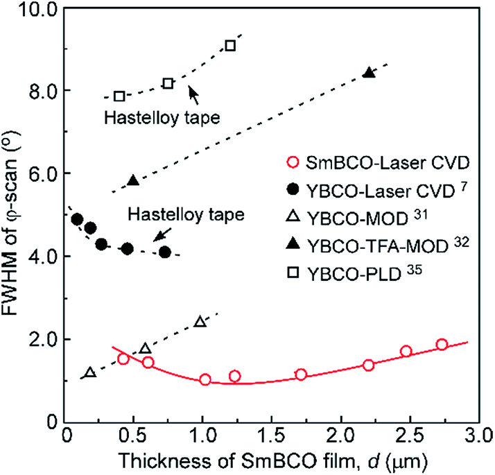 | ||
| Fig. 5 FWHM of φ-scan of SmBCO and YBCO films deposited by different methods as a function of thickness. | ||
Fig. 6 exhibits the surface and cross-sectional SEM images of SmBCO films with different thicknesses. When the thickness was 0.47 μm, the SmBCO film had a ravine-like surface with some small grains, as shown in Fig. 6(a). The surface became smooth at the thickness of 1.06 μm, which indicated the typical c-axis morphology.26 With the increasing thickness, some round outgrowth and needle-like grains were formed on the dense surface (Fig. 6(c) and (d)). The round outgrowth grains were identified as the Ba–Cu–O compound by EDS, corresponding to the BaCuO2 phase measured by XRD. On the basis of previous studies, the needle-like structure was identified as the a-axis oriented SmBCO grains.36 The cross-sectional SEM images of the SmBCO films are shown in Fig. 6(e)–(h). All the specimens had a dense and uniform structure without visible signs of pinholes or grain boundaries.
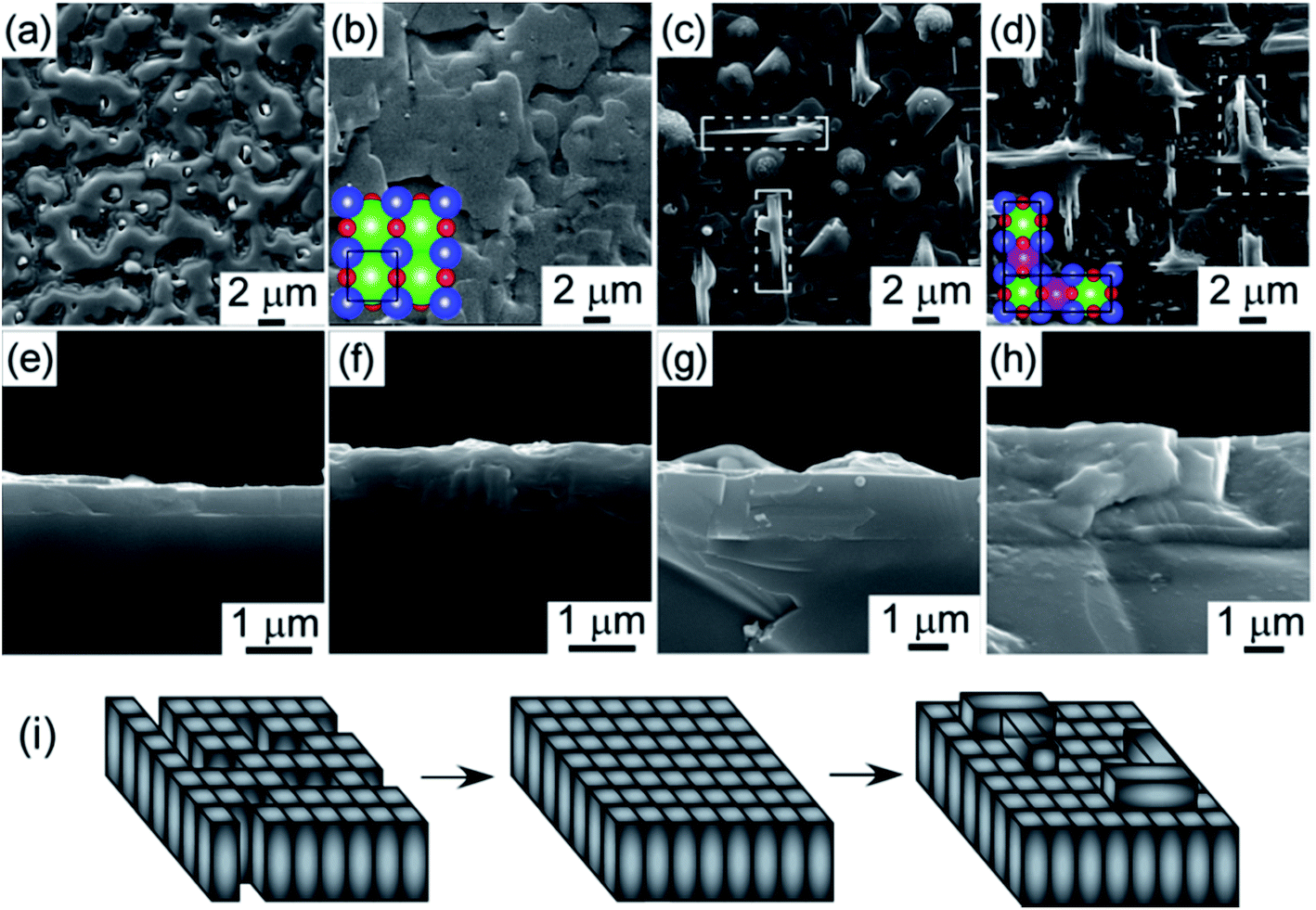 | ||
| Fig. 6 Surface and cross-sectional SEM images of SmBCO films prepared on LAO substrate with d = (a and e) 0.47, (b and f) 1.06, (c and g) 1.71 and (d and h) 2.72 μm, and (i) growth model of the SmBCO film. | ||
An illustration for the growth model of the SmBCO film is displayed in Fig. 6(i). The c-axis-oriented crystallinity nuclei were formed first as islands or kinks under the influence of a single crystalline LAO substrate; then, the nuclei coalesced, and the c-axis-oriented film finally deposited. However, with the increasing thickness, the a-axis grain formed at the late deposition stage. In previous literature, a cooling of the film surface was considered as a possible origin for the nucleation of a-axis-oriented grains.9 In the present study, the surface temperature of the film remained constant during the deposition process by laser CVD because the laser always heated the top surface of the film, and the laser power was controlled precisely and automatically under the feedback of a pyrometer. We speculated that the a-axis grain might have formed at the late deposition stage because the restriction of the substrate became weak with the increasing thickness, and the growth rate along the a-axis was faster than that along the c-axis.8,9,29
Fig. 7 shows the cross-sectional TEM images and the SAED pattern of the c-axis-oriented SmBCO film with d = 1.06 μm. The clear interface of the SmBCO film and LAO substrate further confirmed that the SmBCO film had a dense structure with no visible pinholes (Fig. 7(a)). The dense and epitaxial structure was beneficial for improving the critical current of the film, which was of great significance for the high current applications of SmBCO thick films.37 The high resolution TEM (HRTEM) image of the interface between the SmBCO film and LAO substrate indicated that the growth of the film was initiated on the LAO substrate with a strong epitaxial alignment (Fig. 7(b)). The lattice distance was about 0.39 nm, which was close to the lattice distance of the SmBCO (100) plane (a = 0.3851 nm). Fig. 7(d) shows that the SmBCO film had a c-axis direction normal to the LAO substrate according to the SAED pattern of area (B) in Fig. 7(a). The in-plane orientation of the SmBCO film and LAO substrate was SmBCO[100]//LAO[010] and SmBCO[010]//LAO[001], which was consistent with the results obtained by the pole figure (Fig. 4(a)). In Fig. 7(c), the HRTEM of area (C) in Fig. 7(a) shows the single-crystalline structure without grain boundary. The SAED pattern of area (C) in Fig. 7(a) (Fig. 7(e)) had the same direction with interface in Fig. 7(d); this implied that the c-axis orientation of film was retained with the increasing thickness.
 | ||
| Fig. 7 Cross-sectional TEM images and the SAED pattern of the SmBCO film with d = 1.06 μm: (a) low magnification TEM, (b) HRTEM and (d) SAED pattern of the area (B) in (a) and LAO substrate, (c) HRTEM, and (e) SAED pattern of area (C) in (a). | ||
Fig. 8 displays the temperature dependence of electrical resistivity (R) of the SmBCO thick films at d = 0.47, 1.06, and 2.72 μm. The R of the SmBCO films at d = 0.47 μm with c-axis-orientation showed metallic temperature dependence at normal state and sharp zero resistance transition at critical transition temperature (TC) of 83 K. As the thickness of the SmBCO film increased to 1.06 μm, TC increased to 89.5 K. The R of the SmBCO film with d = 2.72 μm showed a semiconductive resistivity behavior at high temperatures and then decreased to zero. The current has been known to travel on the CuO2-plane that parallels the ab-plane in the c-axis-oriented SmBCO film. The SmBCO film with d = 2.72 μm had a host of twinned a-oriented grains, which might impede the electrical conduction along the film surface. The results showed that the SmBCO film with d = 1.06 μm possessed the highest TC.
 | ||
| Fig. 8 Temperature dependence of resistivity of the SmBCO films with different thicknesses. | ||
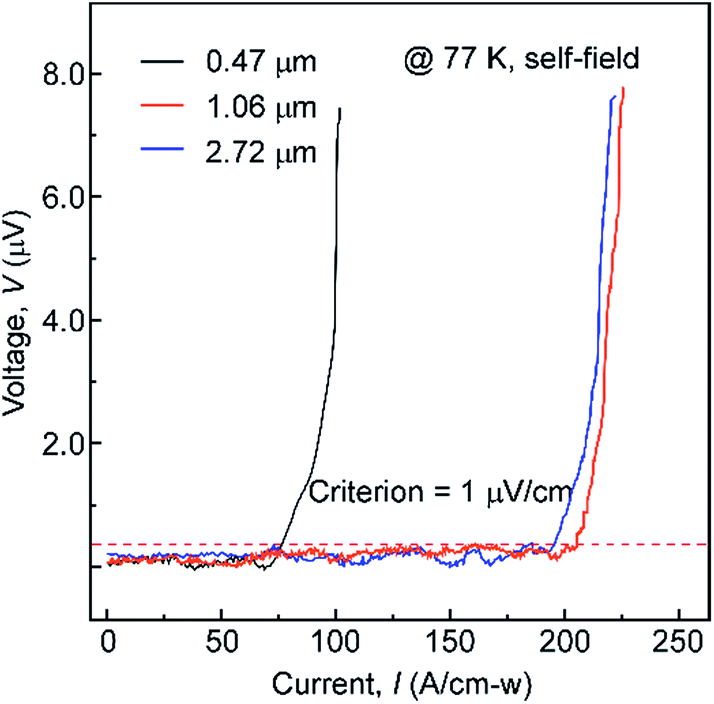
Fig. 9 shows the current–voltage (I–V) curve (77 K and self-field) for SmBCO films with different film thicknesses. The IC of the SmBCO film with d = 0.47, 1.06, and 2.72 μm reached 76, 204, and 196 A cm−1-W (corresponding to JC = 1.62, 1.92, and 0.72 MA cm−2) with the criterion of 1 μV cm−1, respectively. The SmBCO film with d = 1.06 μm had the highest IC and JC. As the thickness increased from 0.47 to 1.06 μm, JC increased from 1.62 to 1.92 MA cm−2 due to the better crystallization. The decrease of the JC for the film thicker than 1.06 μm may be due to the a-axis oriented grains and impurity phases in the film.8,9
 | ||
| Fig. 9 Current–voltage (I–V) curve for the SmBCO films with different thicknesses (77 K and self-field). | ||
Fig. 10 shows the comparison of IC and JC of SmBCO and YBCO films reported in literature at 77 K under self-field.12,29,32 In Fig. 10(a), all the IC values of SmBCO and YBCO films first increased and then decreased with the increasing thickness. It was noteworthy that the IC of the SmBCO film deposited by laser CVD only decreased slightly with the increasing thickness as compared to the case of the films deposited by other methods.12,29,32 The crystallinity of the SmBCO film deposited by laser CVD was poor since the grains didn't have enough time to arrange orderly at high deposition rates; this resulted in lower IC than that of the YBCO film deposited by MOCVD. From Fig. 10(b), it can be seen that JC values of SmBCO and YBCO deposited by MOCVD decline deeply.12,29,32 The JC of YBCO deposited by TFA-MOD was lower than that of the SmBCO film deposited by laser CVD. The out-plane and in-plane crystallinity of the SmBCO film deposited by laser CVD was improved with the increasing thickness; this contributed to an increase of JC.7
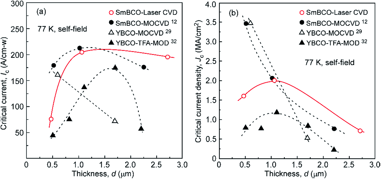 | ||
| Fig. 10 Comparison of (a) IC and (b) JC of SmBCO and YBCO films with respect to the film thickness (77 K and self-field). | ||
4. Conclusions
SmBCO films with different thicknesses (d) in the range from 0.47 to 2.72 μm were prepared on LAO by laser CVD with an average deposition rate of 7.6 μm h−1. The SmBCO film was c-axis oriented at d ≤ 1.06 μm, and a-axis-oriented grains appeared at d ≥ 1.71 μm. The JC of the SmBCO film was related to the out-plane and in-plane crystallinity, i.e., the lower the FWHM of φ-scan, the higher the JC. The SmBCO film with d = 1.06 μm had both the highest TC of 89.5 K and JC of 1.92 MA cm−2 (corresponding to IC = 204 A cm−1-W).Conflicts of interest
There are no conflicts of interest to declare.Acknowledgements
This work was supported by the National Natural Science Foundation of China (No. 51372188, and 51521001) and by the 111 Project (B13035). This research was also supported by the International Science & Technology Cooperation Program of China (2014DFA53090) and the Natural Science Foundation of Hubei Province, China (2016CFA006), and the National Key Research and Development Program of China (2017YFB0310400), and the Fundamental Research Funds for the Central Universities (WUT: 2017II43GX, 2017III032, 2017YB004), and Science Challenge Project (No. TZ2016001), and the State Key Laboratory of Advanced Technology for Materials Synthesis and Processing (WUT, Grant No: 2017-KF-5).References
- J. V. J. Congreve, Y. H. Shi, A. R. Dennis, J. H. Durrell and D. A. Cardwell, J. Am. Ceram. Soc., 2016, 99, 3111–3119 CrossRef CAS.
- H. S. Kim, S. S. Oh, N. J. Lee, S. H. Jang, C. H. Min, H. S. Ha, K. C. Chung, D. J. Youm, S. H. Moon and C. Park, Phys. C, 2011, 471, 932–936 CrossRef CAS.
- Y. Shiohara, T. Taneda and M. Yoshizumi, Jpn. J. Appl. Phys., 2012, 51, 10007 CrossRef.
- X. O. Institut and T. Puig, Supercond. Sci. Technol., 2014, 27, 44003 CrossRef.
- B. Tao, N. Zhang, F. Zhang, Y. Xia, X. Feng, Y. Xue, X. Zhao and J. Xiong, IEEE Trans. Appl. Supercond., 2011, 21, 2945–2948 CrossRef CAS.
- Y. Takahashi, Y. Yoshida, Y. Ichino, Y. Takai, M. Yoshizumi, T. Izumi and Y. Shiohara, Phys. C, 2011, 471, 937–939 CrossRef CAS.
- P. Zhao, A. Ito and T. Goto, J. Electroceram., 2014, 34, 137–141 CrossRef.
- S. Sieve, F. Mattheis, H. U. Krebs and H. C. Freyhardt, J. Appl. Phys., 1995, 78, 5545–5548 CrossRef.
- A. Ibi, H. Iwai, K. Takahashi, T. Muroga, S. Miyata, T. Watanabe, Y. Yamada and Y. Shiohara, Phys. C, 2005, 431, 910–914 CrossRef.
- K. J. Leonard, A. Goyal, D. M. Kroeger, J. W. Jones, S. Kang, N. Rutter, M. Paranthaman and D. F. Lee, J. Mater. Res., 2003, 18, 1109–1122 CrossRef CAS.
- T. Ozaki, Y. Yoshida, M. Miura, Y. Ichino, Y. Takai, K. Matsumoto, A. Ichinose, S. Horii and M. Mukaida, Phys. C, 2007, 465, 649–652 CrossRef.
- A. Abrutis, A. Bartasyte, Z. Saltyte, A. Zukova, S. Donet and F. Weiss, Phys. C, 2004, 415, 21–28 CrossRef CAS.
- F. M. Granozio, M. Salluzzo and U. S. Uccio, Phys. Rev. B: Condens. Matter Mater. Phys., 2000, 61, 756–765 CrossRef.
- F. M. Granozio and U. S. di Uccio, J. Cryst. Growth, 1997, 174, 409–416 CrossRef.
- G. Majkic, E. Galstyan and V. Selvamanickam, IEEE Trans. Appl. Supercond., 2015, 25, 6605304 CrossRef.
- T. Wang, R. Tu, W. Ke, S. Zhang, L. Zhang and G. Takashi, J. Wuhan Univ. Technol., Mater. Sci. Ed., 2016, 31, 15–19 CrossRef CAS.
- C. S. Chern, J. Zhao, Y. Q. Li, P. Norris, B. Kear, B. Gallois, Z. Kalman, C. S. Chern, J. Zhao, Y. Q. Li, P. Norris, B. Kear and B. Gallois, Appl. Phys. Lett., 1991, 58, 185–187 CrossRef CAS.
- O. Hiroshi, K. Yoshihiko, K. Minoru, H. Susumu, H. Harima and T. Kunihide, Jpn. J. Appl. Phys., 1990, 29, 1070–1075 CrossRef.
- S. Zhang, R. Tu and T. Goto, J. Am. Ceram. Soc., 2012, 95, 2782–2784 CrossRef CAS.
- H. Cheng, R. Tu, S. Zhang, M. Han, T. Goto and L. Zhang, J. Eur. Ceram. Soc., 2017, 37, 509–517 CrossRef CAS.
- P. Zhu, Q. Xu, R. Chen, S. Zhang, M. Yang, R. Tu, L. Zhang, T. Goto, J. Yan and S. Li, J. Am. Ceram. Soc., 2017, 100, 1634–1641 CrossRef CAS.
- P. Zhao, A. Ito, R. Tu and T. Goto, Supercond. Sci. Technol., 2010, 23, 125010 CrossRef.
- F. K. Lotgering, J. Inorg. Nucl. Chem., 1959, 9, 113–123 CrossRef CAS.
- S. Matsuno, F. Uchikawa, S. Utsunomiya and S. Nakabayashi, Appl. Phys. Lett., 1992, 60, 2427–2429 CrossRef CAS.
- Y. Ma, K. Watanabe, S. Awaji and M. Motokawa, J. Appl. Phys., 2000, 39, L726–L729 CAS.
- E. H. Sujiono, P. Arifin and M. Barmawi, Mater. Chem. Phys., 2002, 73, 47–50 CrossRef CAS.
- A. Molodyk, M. Novozhilov, S. Bitkowsky, S. Street, A. Delaney and L. Castellani, IEEE Trans. Appl. Supercond., 2009, 19, 3196–3199 CrossRef CAS.
- J. Xiong, F. Zhang, X. Liu, R. Zhao, X.-H. Zhao and B.-W. Tao, Rare Met., 2014, 33, 70–74 CrossRef CAS.
- L. Vergnières, S. Donet, C. Jimenez, P. Odier, F. Weiss, C. E. Bruzek and J. M. Saugrain, IEEE Trans. Appl. Supercond., 2005, 15, 2759–2762 CrossRef.
- Y.-L. He, G.-C. Wang, A. J. Drehman and H.-S. Jin, J. Appl. Phys., 1990, 67, 7460–7466 CrossRef CAS.
- S. Ghalsasi, Y. X. Zhou, J. Chen, B. Lv and K. Salama, Supercond. Sci. Technol., 2008, 21, 45015 CrossRef.
- S. H. Jang, J. H. Lim, J. S. Lee, K. M. Yoon, K. T. Kim, J. Joo, S. Jung and H. Lee, Phys. C, 2007, 451, 118–126 CrossRef CAS.
- P. Zhao, A. Ito and T. Goto, Ceram. Int., 2014, 40, 2057–2061 CrossRef CAS.
- D. Guo, A. Ito, R. Tu and T. Goto, Appl. Surf. Sci., 2012, 259, 178–185 CrossRef CAS.
- H. Zhang, J. Yang, S. Wang, Y. Wu, Q. Lv and S. Li, Phys. C, 2014, 499, 54–56 CrossRef CAS.
- S. Li, W. Li, G. Li, W. Li, B. Zhang and P. Chou, Phys. C, 2012, 478, 60–66 CrossRef CAS.
- R. Knibbe, N. M. Strickland, S. C. Wimbush, A.-H. Puichaud and N. J. Long, Supercond. Sci. Technol., 2016, 29, 66006 CrossRef.
| This journal is © The Royal Society of Chemistry 2017 |