
 Open Access Article
 This Open Access Article is licensed under a Creative Commons Attribution-Non Commercial 3.0 Unported Licence
Preparation and flash memory performance based on fluorene–triphenylamine copolymer (PF–TPA)/MWCNTs†
Qun Yanga,
Xiankai Jianga,
Ying Xina,
Xiaofeng Zhaoc,
Jiahe Huanga,
Shuhong Wang *a,
Rongrong Zhengb,
Dongge Mad and
Cheng Wang*ab
*a,
Rongrong Zhengb,
Dongge Mad and
Cheng Wang*ab
aKey Laboratory of Functional Inorganic Material Chemistry, Heilongjiang University, Harbin 150080, P. R. China. E-mail: wangc_93@163.com; openair@163.com
bSchool of Chemical Engineering and Materials, Heilongjiang University, Harbin 150080, P. R. China
cSchool of Electronic Engineering, Heilongjiang University, Harbin 150080, P. R. China
dSchool of Materials Science and Engineering, South China University of Technology, Guangzhou 510640, P. R. China
First published on 28th November 2017
Abstract
A conjugated alternating polymer based on fluorene and triphenylamine, namely poly[(9,9-dioctyl)-2,7-fluorene-co-triphenylamine] (PF–TPA), in which triphenylamine (TPA) as electron donor and hole transporting group was devised and synthesized on the basis of the Suzuki coupling method. The structural properties of the copolymer can be verified by Fourier transform infrared (FT-IR) spectroscopy, hydrogen and carbon nuclear magnetic resonance (1H-NMR, 13C-NMR). Nonvolatile memory devices with bistable electrical switching behavior were observed based on active layers of both fluorene–triphenylamine copolymer (PF–TPA) and PF–TPA:carbon nanotubes (CNTs) hybrid composite materials. Typical formed composite-based device with sandwich configuration, indium tin oxide (ITO)/PF–TPA:CNTs/Al, was demonstrated superior rewritable flash memory property compare to the ITO/PF–TPA/Al device with a greater ON/OFF state current ratio. In addition, the optimal storage characteristics occurs when the doping concentration of CNTs was at a certain value (CNTs = 0.3 mg mL−1), which leading to the ON/OFF state current ratio added up to 2 orders of magnitude and the switching threshold voltage reduced prominently. The conductance switching mechanism of devices was also further discussed. After testing, the devices have good stability and durability, which have a potential application value in data storage.
1. Introduction
Resistive random access memory (RRAM) based on organic films with resistive switching effects has attracted intense attention from scholars in the recent two decades.1 Owing to the advantages of easy processing, high storage density, low cost, low power consumption, and high mechanical flexibility,2–5 organic storage, which is different from traditional semiconductor silicon based electrical memory,6 has become an emerging electrical memory technology and has developed rapidly.7 Generally speaking, the organic resistive memories realize the transition of different conducting states by applying an external voltage to both ends of the organic functional layer film, and the OFF state and ON state are equivalent to the “0” and “1” in binary systems.8 Moreover, nanocomposite materials, because of their attractive properties, were considered as a promising candidate for the next generation of nonvolatile memory devices, and the addition of inorganic nanomaterials further optimizes the electrical and optical properties of the matrix, promoting organic polymer/inorganic nanocomposite materials with broad commercial development and application prospects.9–11In recent years, polymers and their composites with carbon nanotubes have been gradually applied to the field of organic electronics memory which due to the unique hybrid structure and attractive physical properties of carbon nanotubes.12–14 Large numbers of RRAM based on polymers have been developed by adding carbon nanotubes, including poly(N-vinylcarbazole) (PVK),15 polyvinyl alcohol (PVA),16 poly-4-vinyl-phenol (PVP),17 poly(3,4-ethylenedioxythiophene):poly-(styrenesulfonate) PEDOT:PSS,18,19 epoxy methacrylate resin (EMAR),20 polyurethane (PU).21 These researches made different attempts to mix carbon nanotubes into organic films and reasonable conjecture that the amount of carbon nanotubes doped cause some memories exhibited distinctly different resistance behaviors. For example, G. Liu et al. found that the device produces insulator behavior (0.2% CNTs), bistable electrical switching behavior (0.5–2% CNTs), and conductor behavior (≥3% CNTs)15 by manipulating the content of carbon nanotubes in the PVK layers; then Pandurangan et al. once again confirmed the three similar electrical behaviors of PVA film joined with 0.1% CNTs, 1–3% CNTs and ≥5% CNTs, respectively.16 In addition, a current bistability was shown in the PEDOT:PSS matrix with a small quantity of functionalized multiwalled carbon nanotubes (MWCNTs) (≤0.01 wt%).18 Subsequently, researchers continued to investigate the effects of different levels of SWCNTs on the bi-directionally memory behavior in the identical matrix,19 nonvolatile memory characteristics in EMAR + CNTs and PU + CNTs composite film have gradually been developed.20,21 Although much work has been reported on the effects of electrical switching and memory effects in doped or mixed polymer with inorganic nanoparticles systems, the influence of dope level on the conductance behavior of polymeric composites seems to be worth further exploration.22,23
As the hole-transporting materials, polyfluorene (PF) and its derivatives have become one of the most promising candidates for organic memory devices (OMDs).24 The fluorene group, as a good luminescent material, has higher carrier mobility and carrier transport along its conjugated backbone.25,26 The triphenylamine (TPA) group in the main chain was used as electron donor, which helped to enhance the hole transport ability and thermal stability of the polymer, was a typical hole transporting material.27 Therefore, copolymer containing fluorene or triphenylamine groups have attracted considerable attention as electrical storage materials.28,29 In this study, we first synthesized the conjugated alternating copolymer poly[(9,9-dioctyl)-2,7-fluorene-co-N-4,4′-triphenylamine] (i.e., PF–TPA) by Suzuki coupling reaction and characterized the copolymer by various tests. Then the nonvolatile bistable conductor switching behavior and rewritable flash memory effects in both ITO/PF–TPA/Al and ITO/PF–TPA:CNTs/Al memory devices were discovered. The performance of the nonvolatile memory, which fabricated by the PF–TPA + CNTs with different doping levels as an active layer, improved to a certain extent compared with the ITO/PF–TPA/Al device. It can be obviously perceived that the electrical memory characteristics was significantly improved with the higher ON/OFF current ratio (increased from 102 to 104) and lower threshold voltage (VSET reduced from −2.4 V to −1 V) in a specific concentration (CNTs = 0.3 mg mL−1) by adding CNTs into PF–TPA matrix. No significant attenuation occurs in current during the retention and endurance tests illustrated that the presence of CNTs enables the device to remain stable. Finally, the electrical characteristics were analyzed by reasonable simulation and our fabricated devices exhibits preeminent flash and reliability characteristics.
2. Experimental
2.1 Materials
All of the organic solvents and reagents were purchased from Sinopharm Co. Ltd. The sodium carbonate was dehydrated and the toluene was distilled over sodium under dry nitrogen. MWCNTs were disposed by acidification treatment. The outer diameter of the tube was 17–23 nm and the length of the tubes was several μm. The micro-structure analysis of CNTs was exposed by means of transmission electron microscopy (TEM) research, as shown in Fig. S1.† All other chemicals were provided by Sigma-Aldrich without further purified.2.2 Synthesis of poly[(9,9-dioctyl)-2,7-fluorene-co-triphenylamine] (PF–TPA)
Scheme 1 shows the synthetic route and the chemistry structure of PF–TPA. 9,9′-Dioctyfluorene-2,7-diboronic acid bis(1,3-propanediol)ester (0.5000 g, 0.8954 mol), 4,4′-dibromotriphenylamine (0.3608 g, 0.8954 mmol) and toluene (14 mL) were added into a flask which was by removal of water and deoxidization in advance. After the reaction mixture was dissolved, tetrakis(triphenylphosphine)palladium(0) [Pd(PPh3)4] (0.0310 g, 2.686 × 10⁻² mmol) as catalyst and sodium carbonate solution (3 mol L−1, 14 mL) were added into the flask rapidly, accompanied with the gradual heating from 95 °C to 105 °C and kept stirring and refluxing under nitrogen atmosphere for 48 h. The organic layer was washed several times with deionized water and concentrated by rotatory evaporator after the solution cooled, then dropped the obtained product into methyl alcohol to precipitate the desired product. The product was accumulated by negative-pressure filtration and washed with methyl alcohol. Finally the copolymer was extracted by acetone in soxhlet extractor for 48 h to remove the remaining monomers and Pd catalyst and dried in a vacuum dying oven. The dried product was characterized by FT-IR spectroscopy, 1H-NMR and 13C-NMR analyzes.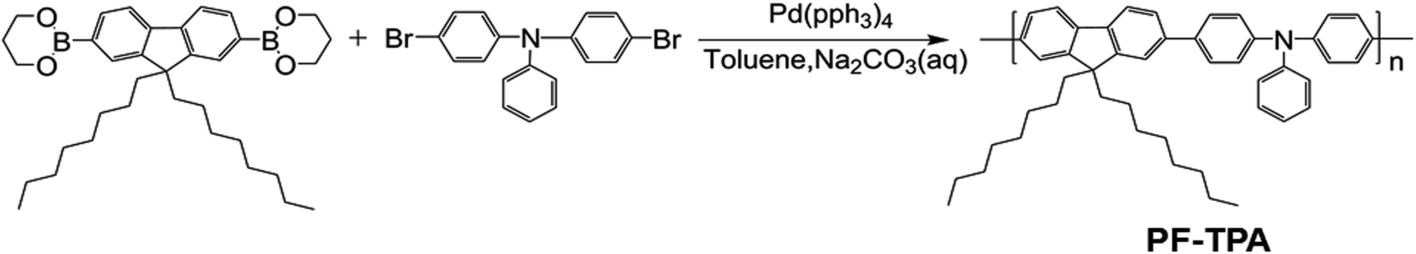 | ||
| Scheme 1 Synthesis routes and the chemistry structure of copolymer (PF–TPA). | ||
2.3 Fabrication of the memory device
Before spin-coating the film, the indium tin oxide (ITO) conductive glass of dimension 2 cm × 1 cm (sheet resistance R ≤ 10 Ω □−1) were preprocessed gradually with deionized water, abstergent, acetone and ethanol for 30 min each by ultrasonication and stored in a vacuum drying oven at 60 °C for 12 h. The PF–TPA (Mw = 26![[thin space (1/6-em)]](https://www.rsc.org/images/entities/char_2009.gif) 000) with different carbon nanotubes doping content is used as the active layer of the device. Synthetic copolymer PF–TPA was dissolved in toluene with stirring and filtered through a 0.22 μm pore size of polytetrafluoroethylene membrane syringe filter to prepare a homogeneous solution.
000) with different carbon nanotubes doping content is used as the active layer of the device. Synthetic copolymer PF–TPA was dissolved in toluene with stirring and filtered through a 0.22 μm pore size of polytetrafluoroethylene membrane syringe filter to prepare a homogeneous solution.
For manufacture the blended composites, MWCNTs was disperse in isopropanol and keep ultrasonication for 50 min. Afterwards, the same volume of MWCNTs dispersion and the pretreatment of PF–TPA solution were mixed together and persistently stirred for 1 h. Different dosages of mixture as composite film samples were shown in Table 1, which were spin-coated onto the ITO conductive glass substrate at a rotate speed of 900 rpm for 15 s and then 3000 rpm for 45 s.
| Sample | CNTs (mg) | PF–TPA (mg) | Isopropyl alcohol (mL) | Toluene (mL) |
|---|---|---|---|---|
| A | 0 | 5 | 0 | 1 |
| B | 0.1 | 5 | 1 | 1 |
| C | 0.3 | 5 | 1 | 1 |
| D | 0.5 | 5 | 1 | 1 |
| E | 1.0 | 5 | 1 | 1 |
After that, the semi-finished films were dried in a vacuum oven at 60 °C for 2 h to get rid of remaining solvent. The film thickness of pure PF–TPA and PF–TPA:CNTs composite were revealed by scanning electron microscope (Hitachi S3400) measurement before vacuum aluminizing. Al electrode was used in vacuum thermally evaporation under a shadow mask at 7.5 × 10⁻⁷ Torr with diameter of 200 μm. The elementary diagram of sandwich-structured device and the chemistry structure of MWCNTs were displayed in Fig. 1.
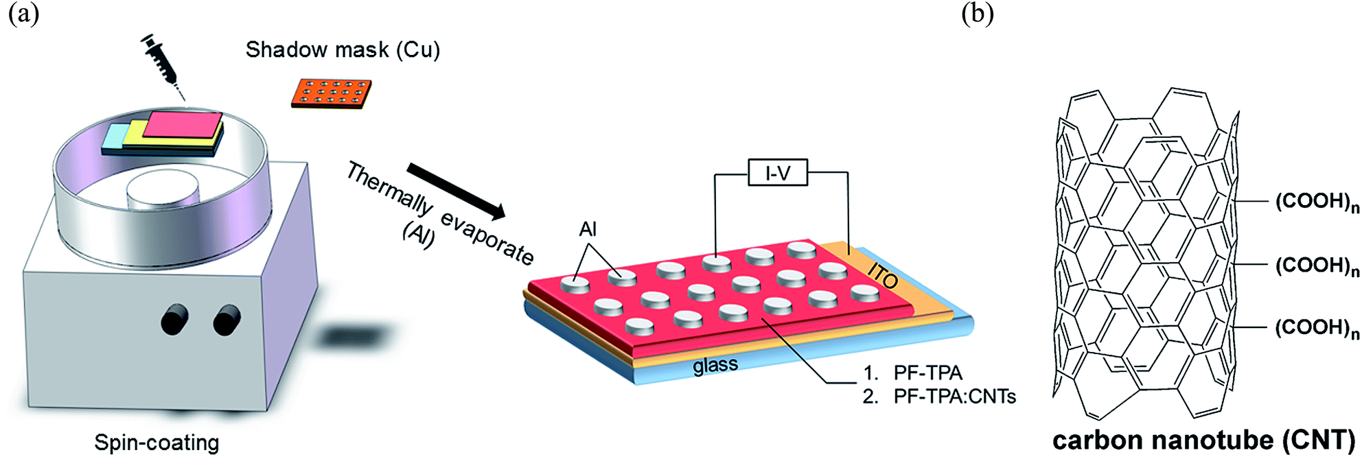 | ||
| Fig. 1 (a) Schematic diagram of the sandwich-structured device. (b) Chemistry structure of carbon nanotube (CNT). | ||
2.4 Measurements
The FT-IR spectra were indicated on Magna-IR560 infrared spectrometers with KBr pellet from 400–4000 cm−1 wavenumbers. 1H NMR and 13C NMR spectra were measured on a Bruker Advance 400 NMR spectrometer with deuterated chloroform as the solvents of 400 MHz resonance frequency. The molecular orbitals were calculated by the density function theory (DFT) using Parr correlation functional method (B3LYP) and the 6-31G basis set. The electrical memory characteristics of the device was disposed on an analytical probe station by a Keithley 4200-SCS semiconductor parameter analyzer at room temperature in the exposed atmospheric environment. Two probes were in contacted with the top electrode (Al) and the grounded bottom electrode (ITO) throughout the whole process of scanning voltage (applied voltage from 6 V to −6 V) with the step of 0.05 V. In the meantime, a current of 0.1 A was exerted in order to keep off the collapse of the device.3. Results and discussion
3.1 Characterization of the copolymer PF–TPA
The dried copolymer PF–TPA was weighed to 0.4667 g and the yield of product is 82.54%. Furthermore, the product was characterized by FT-IR spectroscopy, 1H-NMR and 13C-NMR analyzes.We analyzed the existence of bonds in PF–TPA by FT-IR spectroscopy, in which the instrument was a Magna-ir560 infrared spectrometer, and the results were shown in Fig. S2.† It is found that the characteristic absorption peak in 2922 cm−1 and 2850 cm−1 are due to the C–H stretching vibration of the fluorene in PF–TPA. In addition, the absorption peaks at 1511 cm−1 and 1464 cm−1 wavenumbers are ascribed to the C![[double bond, length as m-dash]](https://www.rsc.org/images/entities/char_e001.gif) C skeleton vibrations of PF–TPA. Moreover, the existence of absorption peaks at 1273 cm−1 is attributed to the C–N stretching vibration in triphenylamine.
C skeleton vibrations of PF–TPA. Moreover, the existence of absorption peaks at 1273 cm−1 is attributed to the C–N stretching vibration in triphenylamine.
The 1H-NMR of PF–TPA was shown in Fig. S3.† 1H-NMR (400 MHz, CDCl3) δH (ppm): 7.75 (d, J = 7.8 Hz, 2H), 7.62–7.55 (m, 8H), 7.31 (t, J = 7.7 Hz, 2H), 7.25–7.21 (m, 6H), 7.07 (t, J = 7.4 Hz, 1H), 2.08–1.99 (m, 4H), 1.29–0.98 (m, 24H), 0.79 (t, J = 7.0 Hz, 6H).
The 13C-NMR of PF–TPA was shown in Fig. S4.† 13C-NMR (100 MHz, CDCl3) δH (ppm): 151.67, 147.57, 146.89, 139.81, 139.35, 135.92, 129.37, 127.86, 127.19, 125.56, 124.53, 124.27, 120.95, 119.94, 55.25, 40.49, 31.79, 30.91, 30.06, 29.22, 23.85, 22.60, 14.06.
Furthermore, the copolymer (Mw = 26000) was characterized by gel permeation chromatography (GPC) using a Malvern instrument which attached to a single refractive index detector (Vis-cotek-VE3580-RI Detector). The THF solution with a flow rate of 1 mL min−1 at 35 °C was used as the mobile phase and the standard samples of polystyrene was used for calibration, that the number-average molecular weight (Mn), weight-average molecular weight (Mw), polydispersity (PDI) and the average degree of polymerization (n) of PF–TPA was identified as 15000, 26000, 1.73 and 23.8, respectively.
3.2 Cross-section characteristics of two types of devices
The film thickness of both composites were revealed by means of scanning electron microscope (SEM) research, as shown in Fig. 2. The sandwich structure of the device can be observed with homogeneous film and well-arranged layers. The thickness of active films of PF–TPA and PF–TPA:CNTs are measured as 95.2 nm and 119 nm, respectively.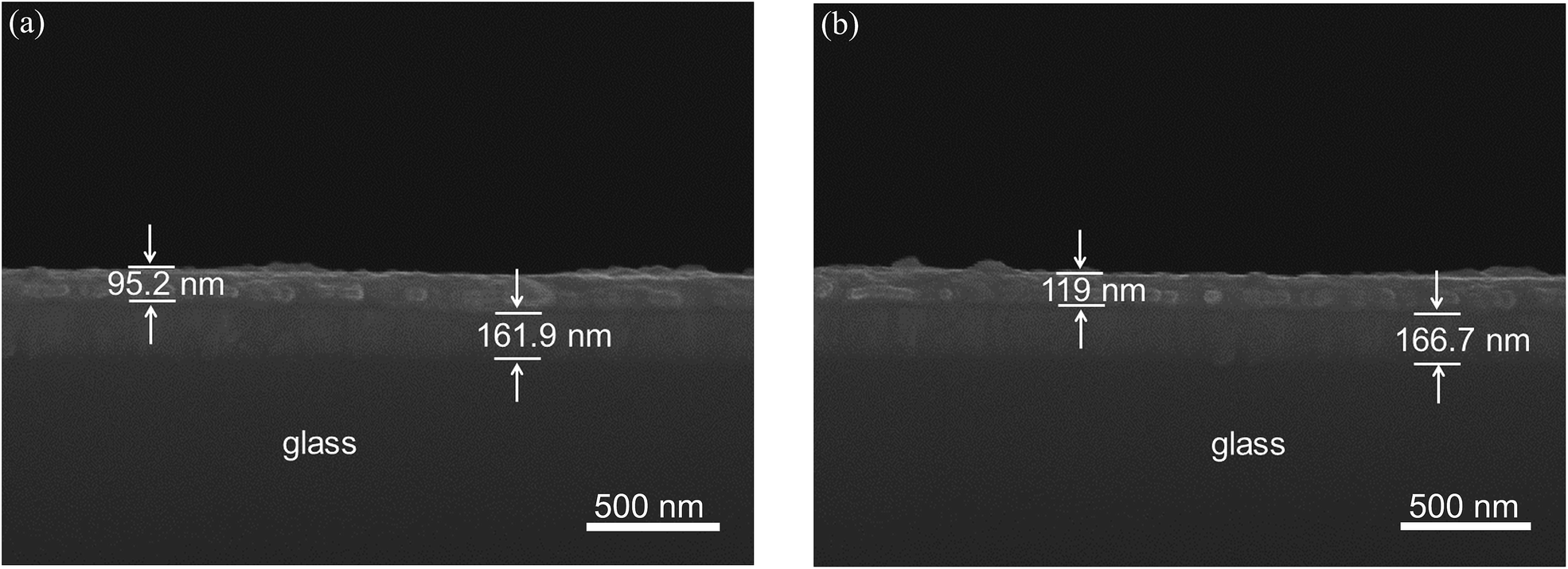 | ||
| Fig. 2 Cross-section scanning electron microscopic images of the device based on (a) PF–TPA and (b) PF–TPA/MWCNTs composite films. | ||
3.3 Characterization of the ITO/PF–TPA/Al memory device
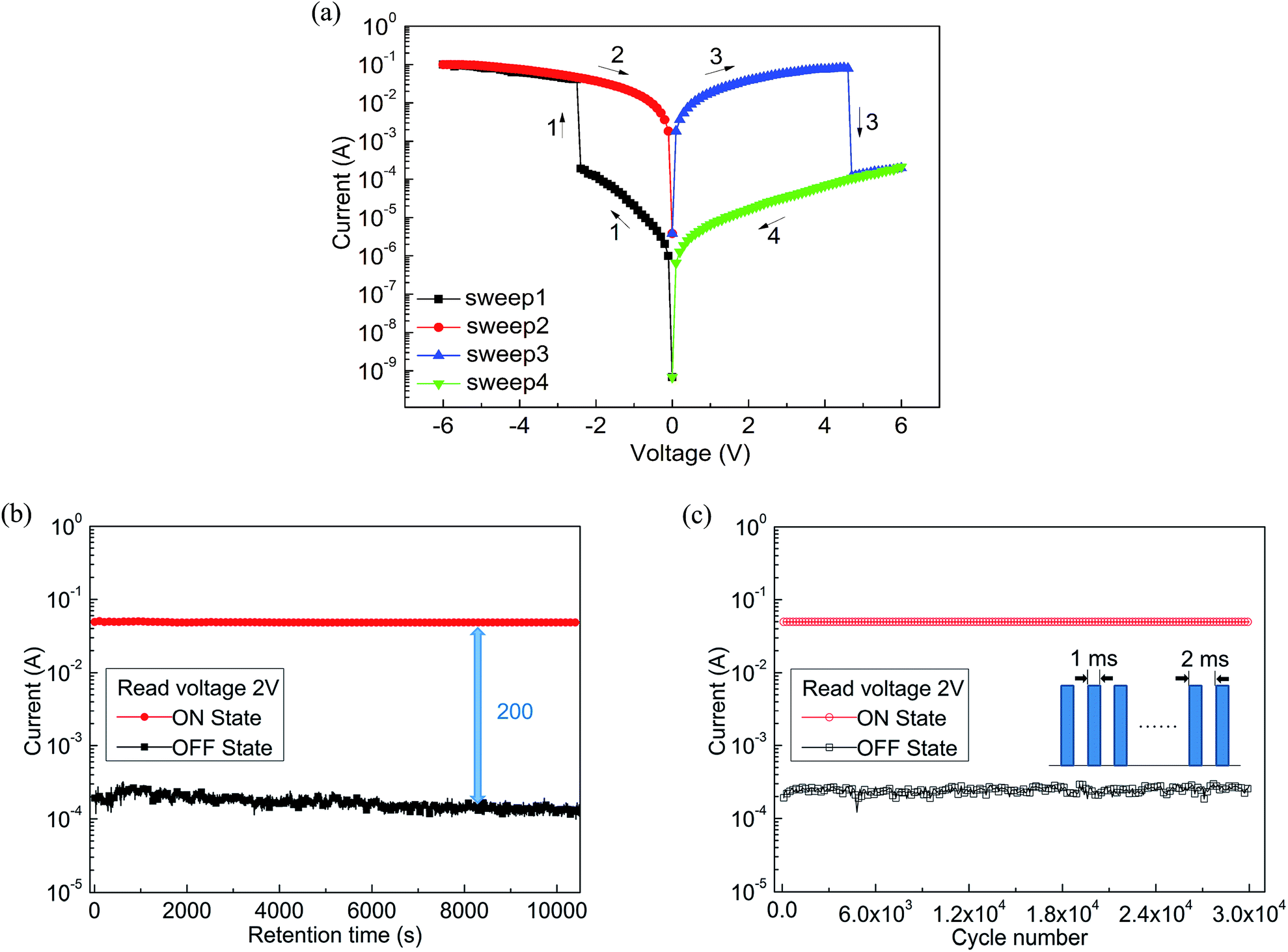 | ||
| Fig. 3 (a) I–V curves, (b) retention performance and (c) endurance performance of ITO/PF–TPA/Al device. | ||
3.4 Characterization of the ITO/PF–TPA:CNTs/Al memory device
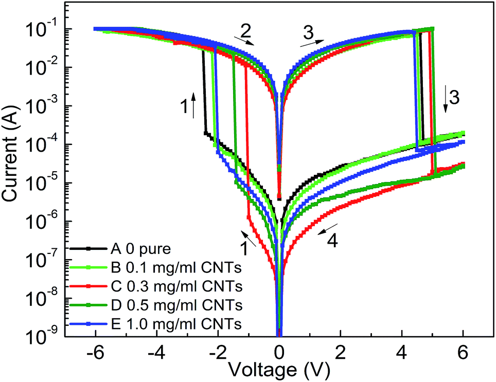 | ||
| Fig. 4 I–V curves of ITO/PF–TPA:CNTs/Al with different CNTs doping level (0 mg mL−1, 0.1 mg mL−1, 0.3 mg mL−1, 0.5 mg mL−1, 1.0 mg mL−1). | ||
Combined with these comparative experiments, we draw the following conclusions. Fig. 5a records the influence of doping concentration both threshold voltage and switching ratio by the double Y curve. The composite device with CNTs shows different levels of electrical memory performance in both threshold voltage and ON/OFF current ratio. Therefore, the incorporation of CNTs was a critical factor to reduce the threshold voltage and increase the switching ratio. Significantly, with the increase of doping level, the ON/OFF current ratio increased and then decreased after reaching a maximum. This may be due to the specific conductivity of CNTs to be well dispersed in film surface to form electron transport pathways. With increasing doping concentration, the effective distance of the isolated CNTs decreases. When the effective distance is less than the diameter of individual carbon nanotube, a homogeneous two-phase interface is favorable for formation to produce more electron transport pathways. When the threshold voltage is approaching, a large number of electrons passing through the increased number of carrier pathways, which cause a switching current ratio increasing phenomenon.15
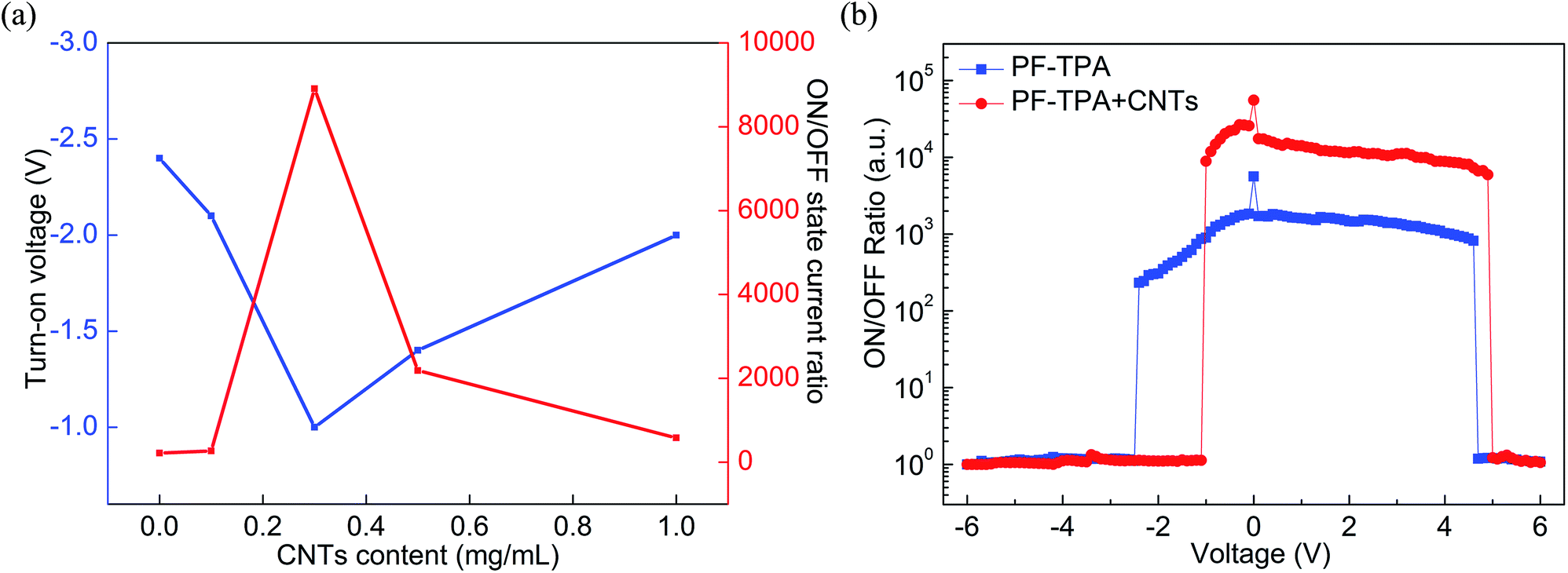 | ||
| Fig. 5 (a) The ON/OFF current ratio and threshold voltage of ITO/PF–TPA:CNTs/Al devices with different CNTs concentration. (b) The ON/OFF current ratio of ITO/PF–TPA:CNTs/Al devices and the ITO/PF–TPA/Al device. | ||
However, we analyze that the excessive concentration dopant will lead to the formation of minimum distances between isolated nanotubes, which affects the charge carrier transport along the electron path and becomes not easy to jump through the nanotube, bringing about a smaller current ratio.15 Meanwhile, the threshold voltage continues to decrease until a minimum value appears at the same concentration. This is because the smaller distance of carbon nanotubes can make effective carrier hopping with lower activation energy.15 Fig. 5b shows the most marked growth in flash window at a given concentration (0.3 mg mL−1) in contrast with the Al/PF–TPA/ITO device as a comparative study.
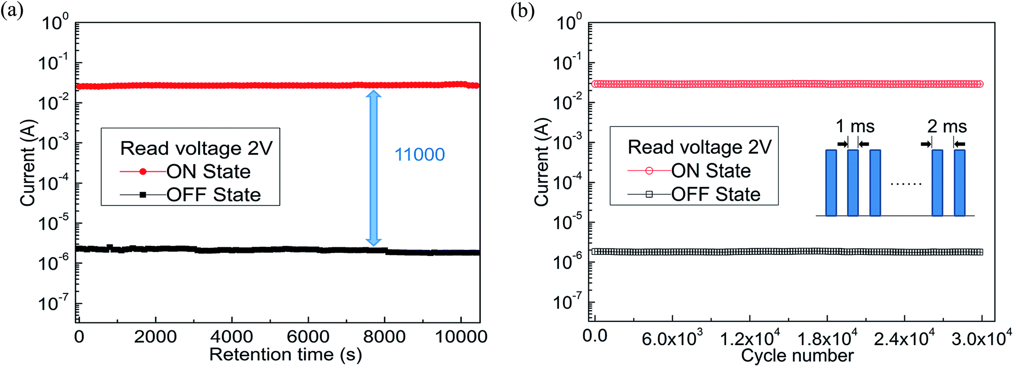 | ||
| Fig. 6 (a) Retention performance and (b) endurance performance of ITO/PF–TPA:CNTs/Al device on sample C. | ||
3.5 Molecular simulation and electronic transition mechanism
The electronic ground state of the copolymer was optimized by DFT, and we can see the theoretical energy level data and the simulation results in the Table 2. The HOMO electron cloud is mainly distributed in the triphenylamine moiety and extended to conjugate chains, suggesting that the TPA unit has a strong electron donating capability for hole migration. And the LUMO electron cloud is concentrated in the conjugated chain of fluorene. The HOMO, LUMO, and the band gap of PF–TPA was calculated to the energy value of −5.00, −1.27 and 3.73 eV by B3LYP/6-31G model chemistry, respectively.
| Frontier molecular orbital | Energy level (eV) | |
|---|---|---|
| HOMO | 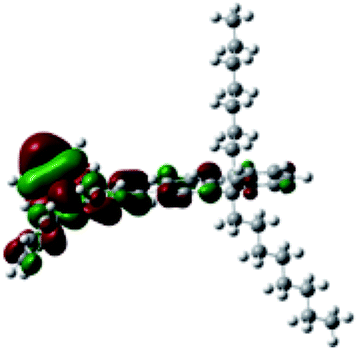 |
−5.00 |
| LUMO | 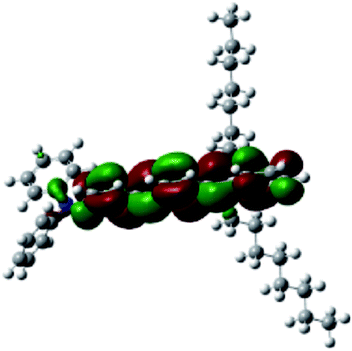 |
−1.27 |
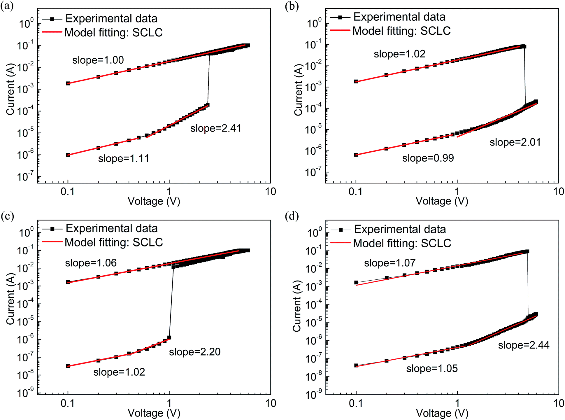 | ||
| Fig. 7 Linear fitting and corresponding slopes for Al/PF–TPA/ITO (a) set, (b) reset and for Al/PF–TPA:CNTs/ITO device based on sample C. (c) Set, (d) reset. | ||
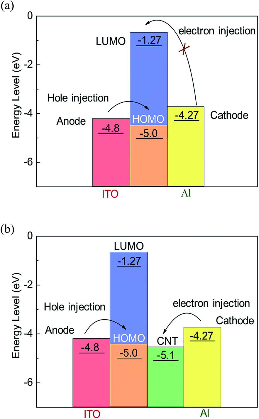 | ||
| Fig. 8 Energy level diagram of the (a) Al/PF–TPA/ITO and (b) Al/PF–TPA:CNTs/ITO sandwich device. | ||
At the other side of Al/PF–TPA:CNTs/ITO, the same conclusion can be inferred from the drawing results in Fig. 7c and d. The appearance of the slope (1.06 and 1.07) gives a phenomenon that the current varies linearly with the applied voltage in the ON state. It means that the relationship abide by the Ohm's law. For OFF state, similar ohmic conduction behavior was also observed under the low voltage location (slop = 1.02 for set and 1.05 for reset) and then transforms into the Child's law with the slope of 2.20 and 2.44 at the high applied voltage. We can also infer that the conductance mechanism is followed the trap-limited space-charge limited current (SCLC) in the Al/PF–TPA:CNTs/ITO device.34,35
In view of the limited charge conduction capacity of polymers, carbon nanotubes are more likely as electron trapping center, introduced into the polymer active films to enhance charge injection and trapping.25,36 As shown in Fig. 8b, in principle, the surfaced-modified CNTs has a work function of −5.1 eV (ref. 38) which is much lower than the LUMO energy level of PF–TPA, it means Al electrode contacts with carbon nanotubes to form an ohmic contact.25 The electron injection from Al electrode into CNT is rather better than hole injection from ITO into the HOMO energy level of PF–TPA. Electrons are first injected from the Al electrode into the CNTs and transmitted along the CNTs axis. Under a certain scan bias, hole injection occurs, the carriers injected into the composite film and is captured by CNTs, resulting in the formation of a space charge layer. When the bias voltage reaches the threshold voltage, the carriers are injected into the polymer LUMO level along the nanotube axis through the film interface, causing a sudden increase in current. The content of CNTs in the device influences the effective distance of the neighboring CNTs, and then urge the trapping behavior of the charge carriers, which makes the devices exhibit different conductive behavior. Correspondingly, the additional heat produced by excessive charge conduction will cause the rupture of the conduction channel formed during the negative bias process, an nonvolatile bistable memory is obtained.
4. Conclusions
To conclude, we have effectively prepared the conjugated copolymers (PF–TPA) by Suzuki coupling reaction and applied to nonvolatile bistable memory device. The ITO/PF–TPA/Al memory device demonstrates excellent electrical storage properties and stability. The ON/OFF current ratio reaches 2 × 10² at low threshold voltage (−2.4 V). In addition, we also fabricated the nonvolatile memory devices utilizing PF–TPA:CNTs composite materials by a spin coating technique and explored the effects of different CNTs concentrations on devices, getting different bistable resistive flash devices. ITO/PF–TPA:CNTs/Al achieves preeminent electrical memory characteristics for that it improves the switching ratio (increased by two orders of magnitude) and reduces the threshold voltage (VSET reduced from −2.4 V to −1 V) with lower error-tolerant rate. Meanwhile, the current remains stable over 3 h in 2 V applied voltage, as well as stable for up to 3 × 10⁴ continuous cycle numbers in 2 V read pulse. The lower threshold voltage, higher switching ratio and excellent stability make the PF–TPA:CNTs composite material have potential application, and occupy the dominant position in the new generation of electrical memory devices.Conflicts of interest
There are no conflicts of interest to declare.Acknowledgements
The authors are grateful to the support of the National Science Foundation of China (51527804, 51473056, 51503058, 51573015, 61471159), Post-graduate Innovative Research Program of Heilongjiang University (YJSCX2015-080HLJU), and Natural Science Foundation of Heilongjiang Province of China (No. B2017010).Notes and references
- Q. Liu, W. H. Guan, S. B. Long, R. Jia and M. Liu, Appl. Phys. Lett., 2008, 92, 012117 CrossRef.
- U. S. Bhansali, M. A. Khan, D. Cha, M. N. AlMadhoun, R. Li, L. Chen, A. Amassian, I. N. Odeh and H. N. Alshareef, ACS Nano, 2013, 7, 10518 CrossRef CAS PubMed.
- J. Y. Ouyang, C. W. Chu, C. R. Szmanda, L. P. Ma and Y. Yang, Nat. Mater., 2004, 3, 918 CrossRef CAS PubMed.
- T. Kurosawa, T. Higashihara and M. Ueda, Polym. Chem., 2013, 4, 16 RSC.
- B. H. Lee, H. Bae, H. Seong, D. I. Lee, H. Park, Y. J. Choi, S. G. Im, S. O. Kim and Y. K. Choi, ACS Nano, 2015, 9, 7306 CrossRef CAS PubMed.
- M. Kanoun, A. Souifi, T. Baron and F. Mazen, Appl. Phys. Lett., 2004, 84, 5079 CrossRef CAS.
- E. J. Yoo, M. Q. Lyu, J. H. Yun, C. J. Kang, Y. J. Choi and L. Z. Wang, Adv. Mater., 2015, 27, 6303 CrossRef.
- G. Khurana, P. Misra and R. S. Katiyar, J. Appl. Phys., 2013, 114, 1625 CrossRef.
- H. Ju and J. Kim, Chem. Eng. J., 2016, 297, 66 CrossRef CAS.
- B. Zhang, Y. Chen, G. Liu, L. Q. Xu, J. Chen, C. X. Zhu, K. G. Neoh and E. T. Kang, J. Polym. Sci., Part A: Polym. Chem., 2011, 50, 378 CrossRef.
- X. Q. Guo, Y. K. Wang and R. Zhang, Adv. Mater. Res., 2013, 634–638, 1943 CrossRef.
- R. H. Baughman, A. A. Zakhidov and W. A. de Heer, Science, 2002, 297, 787 CrossRef CAS PubMed.
- W. J. Yu, A. H. Chae, S. Y. Lee, D. L. Duong and Y. H. Lee, Adv. Mater., 2011, 23, 1889 CrossRef CAS PubMed.
- J. P. Hollingsworth and P. R. Bandaru, Appl. Phys. Lett., 2005, 87, 814 CrossRef.
- G. Liu, Q. D. Ling, E. Y. H. Teo, C. X. Zhu, D. S. H. Chan, K. G. Neoh and E. T. Kang, ACS Nano, 2009, 3, 1929 CrossRef CAS PubMed.
- S. Chandrakishore and A. Pandurangan, RSC Adv., 2014, 4, 9905 RSC.
- W. T. Kim, J. H. Jung and T. W. Kim, Appl. Phys. Lett., 2009, 95, 81 Search PubMed.
- J. A. Ávila-Niño, W. S. Machado, A. O. Sustaita, E. Segura-Cardenas, M. Reyes-Reyes, R. López-Sandoval and I. A. Hümmelgen, Org. Electron., 2012, 13, 2582 CrossRef.
- Y. M. Sun, L. Li, A. Z. Wen, X. D. Bai and G. Li, Phys. Chem. Chem. Phys., 2015, 17, 17150 RSC.
- B. Cho, T. W. Kim, M. Hoe, G. Wng, S. Song and T. Lee, Org. Electron., 2009, 10, 473 CrossRef CAS.
- B. Zhang, Y. L. Liu, Y. Chen, K. G. Neoh, Y. X. Li, C. X. Zhu, E. S. Tok and E. T. Kang, Chem, 2011, 17, 10304 CrossRef CAS PubMed.
- X. Wang, W. Xie and J. B. Xu, Adv. Mater., 2014, 26, 5496 CrossRef CAS PubMed.
- L. Q. Xu, B. Zhang, Y. Chen, K. G. Heoh, E. T. Kang and G. D. Fu, Macromol. Rapid Commun., 2013, 34, 234 CrossRef CAS PubMed.
- H. C. Wu, A. D. Yu, E. Y. Lee, C. L. Liu and W. C. Chen, Chem. Commun., 2012, 48, 9135 RSC.
- G. Liu, Q. D. Ling, E. T. Kang, K. G. Neoh, D. J. Liaw, F. C. Chang, C. X. Zhu and D. S. H. Chan, J. Appl. Phys., 2007, 102, 787 Search PubMed.
- A. Charas, J. Morgado, J. M. G. Martinho, L. Alcácer, S. F. Lim, R. H. Friend and F. Cacialli, Polymer, 2003, 44, 1843 CrossRef CAS.
- Y. Shang, Y. Q. Wen, S. L. Li, S. X. Du, X. B. He, L. Cai, Y. F. Li, L. M. Yang, H. J. Gao and Y. L. Song, J. Am. Chem. Soc., 2007, 129, 11674 CrossRef CAS PubMed.
- T. Kuorosawa, C. C. Chueh, C. L. Liu, T. Higashihara, M. Ueda and W. C. Chen, Macromolecules, 2010, 43, 1236 CrossRef CAS.
- T. W. Kim, S. H. Oh, H. Choi, G. Wang, H. Hwang, D. Y. Kim and T. Lee, Appl. Phys. Lett., 2008, 92, 253308 CrossRef.
- Q. D. Ling, S. L. Lim, Y. Song, C. X. Zhu, D. S. H. Chan, E. T. Kang and K. G. Neoh, Langmuir, 2007, 23, 312 CrossRef CAS PubMed.
- A. A. Nazeer, N. K. Allam, A. S. Fouda and E. A. Ashour, Mater. Chem. Phys., 2012, 136, 1 CrossRef CAS.
- M. Akhtaruzzaman, H. N. M. E. Mahmud, A. Islam, A. E. Shafei, M. R. Karim, K. Sopian, L. Y. Han and Y. Yamamoto, Mater. Chem. Phys., 2013, 142, 82 CrossRef CAS.
- H. Baek, C. Lee, J. Park, Y. Kim, B. Koo, H. Shin, D. Y. Wang and J. Cho, J. Mater. Chem., 2012, 22, 4645 RSC.
- W. Kwon, B. Ahn, D. M. Kim, Y. G. Ko, S. G. Hahm, Y. Kim, H. Kim and M. Ree, J. Phys. Chem., 2011, 115, 19355 CAS.
- G. F. Tian, D. Z. Wu, L. Shi, S. L. Qi and Z. Wu, RSC Adv., 2012, 2, 9846 RSC.
- Q. D. Ling, Y. Song, S. L. Lim, E. Y. H. Teo, Y. P. Tan, C. X. Zhu, D. S. H. Chan, D. L. Kwong, E. T. Kang and K. G. Neoh, Angew. Chem., 2006, 45, 2947 CrossRef CAS PubMed.
- D. C. Guo, Z. Y. Sun, S. H. Wang, X. D. Bai, L. D. Xu, Q. Yang, Y. Xin, R. R. Zheng, D. G. Ma, X. F. Zhao and C. Wang, RSC Adv., 2017, 7, 10323 RSC.
- H. Ago, T. Kugler, F. Cacialli, W. R. Salaneck, M. S. P. Shaffer, A. H. Windle and R. H. Friend, J. Phys. Chem. B, 1999, 103, 8116 CrossRef CAS.
Footnote |
| † Electronic supplementary information (ESI) available. See DOI: 10.1039/c7ra11905d |
| This journal is © The Royal Society of Chemistry 2017 |