
 Open Access Article
 This Open Access Article is licensed under a
 Creative Commons Attribution 3.0 Unported Licence
Manipulating resistive states in oxide based resistive memories through defective layers design†
Zhemi Xu ,
Peiyuan Guan,
Adnan Younis,
Dewei Chu* and
Sean Li
,
Peiyuan Guan,
Adnan Younis,
Dewei Chu* and
Sean Li
School of Materials Science and Engineering, The University of New South Wales, Sydney, NSW 2052, Australia. E-mail: d.chu@unsw.edu.au
First published on 15th December 2017
Abstract
In this work, multilevel switching was achieved by a strategically designed alternative multi-layer structure with pure and Mn-doped SnO2. In this multilayer structure, by utilizing the pure SnO2 layer as an ionic defect diffusion barrier, the migration of ionic defects from the doped layers can be controlled and the intermediate resistance states were stabilized. The multilevel devices exhibit superior performances with a high ON/OFF ratio, low operation voltage and excellent retention. Such an alternative multi-layer structure could be a potential strategy for achieving high-density memories.
Introduction
Recently, resistive random access memories (RRAM) have attracted great interest for potential applications in high-density memories and biological synapses, etc.1–3 RRAMs have distinct advantages over conventional Si based non-volatile memories such as faster response rates, lower power consumption, smaller cell size, mechanical flexibility, transparency, and printablility.4–7 For RRAMs, the figure of merit includes a high ON/OFF ratio,8–10 high-density storage11–13 and long retention time. They are mainly determined by defect migration behaviours driven by applied electrical field, which is associated with the type and concentration of defects.9,14 The high storage density can be achieved either by reducing cell size or increasing storage level. However, the scaling down technology of single cell has approaching their scaling limits.15 Thus, multilevel resistance storage is considered as an important method in developing high-density memories by manipulating ionic defects, and can improve information storage density without decreasing memory cell size.To date, the multilevel resistance states have been achieved by manipulating the applied voltage, such as pulse sequences.16–19 More often, these techniques are too complex or require sophisticated instrumentations that hinder their practical applications. On the other hand, engineering the device structures is another alternative approach to manipulate ionic defects and their kinetics in oxide based films.20 However, to explore engineered design memories for achieving multi-level resistance states in metal oxides is still in its infancy. Controlling the cationic or anionic defects distribution can regulate the ON/OFF ratio and multilevel resistive switching.
In this work, we strategically engineer alternative layered structures to manipulate the defect migration, thus enhancing the ON/OFF ratio and achieving multilevel resistance states. The alternative layer structure has been built by the pristine and doped metal oxides. In the structure, the pristine layer which has less defects acts as diffusion barriers to control the ionic migration in the doped layer. The abundant nature of SnO2 makes this material to be a good representative of wide band-gap metal oxides for the applications of transparent devices, including RRAMs.21,22 The nature defects in SnO2 is known as oxygen vacancies,22,23 which claims as the main factor that contributing the switching behaviour in SnO2. However, due to the limited concentration of oxygen defects, a further improvement in ON/OFF ratio of SnO2 is always desired.24 According to our calculations,25 Mn interstitials (Mnint) with Mn substitutions (Mnsub) is a favourable cation defect in Mn-doped SnO2. Its concentration strongly affects mobility in SnO2. Thus, in this work, pure and Mn-doped SnO2 were utilized as ionic migration barriers and ionic defect providers, respectively.
Experimental
The pure and Mn-doped SnO2 nanocrystals were synthesized through hydrothermal methods and details of synthesis process can be found in our previous report.25 The metal oxide thin film were coated on the silicon substrates by drop coating technique and subsequently dried with ultraviolet irradiation for 4 hours prior to another layer coating as shown in Fig. 1. To fabricate memory cells, gold is used as bottom and top electrodes and deposited by sputtering method.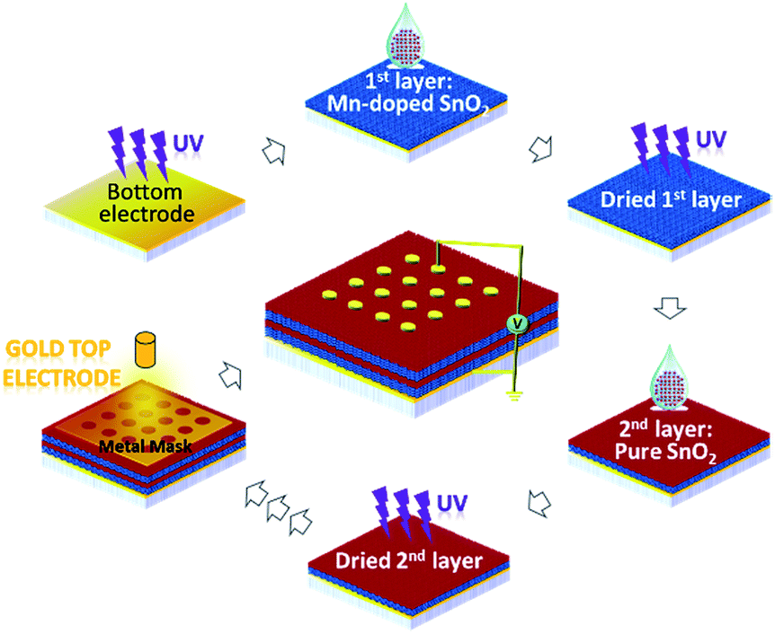 | ||
| Fig. 1 Schematic of multi-layer Mn-doped and pure SnO2 thin film fabrication. | ||
Results and discussion
Characterization
X-ray diffraction spectra of pure and Mn-doped SnO2 thin films were presented in Fig. 2(a). All the diffraction peaks match well with SnO2 (JCPDS #41-1445) without any peaks of the secondary phase. It implies the doped Mn ion is incorporated well in the Sn lattice site, which agrees well with the reported results.26 In the inset of Fig. 2(a), the slight shift in the (110) peak was because of the internal stresses due to the Mn-doping. According to the HRTEM insets in Fig. 2(b) and (c), after Mn-doped, the lattice of SnO2 decreased from 3.38 Å to 3.35 Å, which agrees with the peak shift in XRD. Interestingly, compared to pure SnO2 in Fig. 2(b), the Mn-doped SnO2 nanoparticles in Fig. 2(c) are better self-assembled, which is ideal for thin film deposition.27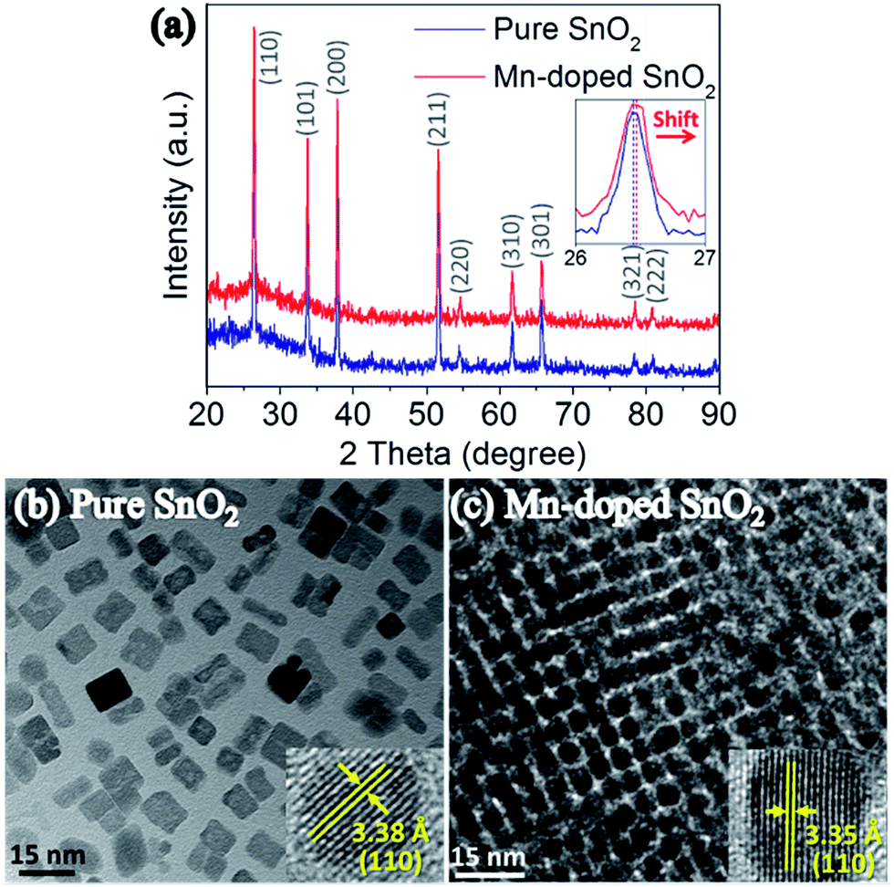 | ||
| Fig. 2 (a) XRD patterns and enlarged (110) peaks of pure and Mn-doped SnO2 thin films; TEM and HRTEM images of (b) pure and (c) self-assembled Mn-doped SnO2 nanoparticles. | ||
Resistive switching in single layer thin films
Resistive switching characteristics of the as-fabricated devices composed of single layered metal oxide were studied first through the current–voltage (I–V) tests with DC voltage sweeping mode. There are three single layer thin film devices being tested here, which are devices composed of pure SnO2 (pure-layer), Mn-doped SnO2 (1-layer) and the mixture of the pure and Mn-doped SnO2 one (mix-layer). During the tests, the bias voltages were applied to the top electrode while keeping the bottom electrode grounded as shown in Fig. 1.The I–V curves of pure-layer is provided in Fig. 3(a). Pure-layer has been switched to ON state. In the testing cycle, the cell was switched from low resistance state (LRS) to high resistance state (HRS) at 4.4 V and then switched back to ON state at a reverse polarity of −2.3 V. It has been reported that oxygen vacancies are the intrinsic defects in SnO2 nanocrystals.22,23 This resistance switching behaviour could be attributed to the migration of oxygen vacancies within two electrodes in the presence of electric potential.28 However, it is hard to distinguish between two states (HRS/LRS = 3.8) during IV curves.
 | ||
| Fig. 3 Voltage–current measurements of single layer (a) SnO2, (b) Mn-doped SnO2, and (c) the SnO2 and Mn-doped SnO2 mixture; schematics of proposed resistance switching model for the single layer thin film switching behaviour of (d) Mn-doped SnO2 and (e) the mixture thin film. | ||
To compare the IV characteristics of Mn-doped SnO2, a device was fabricated with single Mn-doped layer (1-layer) by keeping all other parameters as same. The current–voltage characteristics of the 1-layer device expressed superior resistive switching characteristics over pure layer device as shown in Fig. 3(b). The separation between both resistance states was quite high (HRS/LRS = 243.4) than that of pure-layer. Moreover, the device switches itself to LRS at 1.9 V and then RESET back to HRS at −4.0 V. For 1-layer device, an additional intermediate state was also detected between the ON and OFF states as in Fig. 3(b).
The switching mechanism of the as-fabricated 1-layer device was illustrated in Fig. 3(d). As reported, Mn interstitials with Mn substitutions pair are the most favourite point defects in Mn-doped SnO2, and 6.25% Mn-doping concentration is enough to forming Mnint.25 Thus, Mnint should be the main factor contributing the switching behaviour. Initially, the defects – Mnint were distributed in the film, and the device is in the HRS state. When a voltage applied to the top electrode, the positive charged Mnint generally migrated towards the cathode electrodes, leaving the original interstitial sites as negative charged traps, forming the filament-like conductive paths and switched the thin film to ON state. While the negative voltage is applied, the Mnint ions were pushed back to the surrounding traps, rupturing the migration path ways, which switched the film to OFF state. The intermediate states are associated with lags in formation and blockage process of the Mnint filaments between being switched ON or OFF. The Mnint migration driven by the applied electric field forms filaments to conduct the charge throughout the film. Due to the low Mnint concentration, the energy barrier for the cation migration is relatively high, thus introducing the intermediate states between ON and OFF states. To further investigate the retention property of this intermediate state, data retention test was conducted, and surprisingly, the intermediate state failed to retain its state for longer time, and within 100 seconds, it merged with the more stable LRS as shown in Fig. S-1.† The unstable intermediate states indicate that the device can be switched between ON or OFF within relatively small voltages, therefore, the energy barrier of resistive switching is insufficient to maintain an intermediate state. To increase the ionic migration barriers, pure SnO2 was introduced as a diffusion barrier to control the ionic migration.
To further examine the role of defects and doped layer, another sample was made, in which pure and Mn doped SnO2 nanoparticles were physically mixed together to form a suspension solution. This solution was further used to fabricate a single layer device by following similar method as for previous two devices, attempting to increase the Mnint diffusion barrier by introducing pure SnO2 nanoparticles. The I–V curves are shown in Fig. 3(c). The resistive switching performance of the mixed-layer sample did not show much improvement than both samples. A smaller ON/OFF ratio, and higher SET/RESET voltages were observed (−4.82 V and 4.83 V respectively). In addition, the intermediate states were not observed any more. This may be because by mixing the doped and pure SnO2 nanoparticles, the defect concentration is not high enough to trigger multilevel switching, as illustrated in Fig. 3(e). Therefore, by simply mixing these two nanoparticles, the dispersion of pure SnO2 nanoparticles cannot obstruct the defect diffusion effectively. It indicates that reducing the Mnint concentration cannot effectively control the transportation behaviour and an optimal concentration of Mnint is critical to introduce the intermediate states.
Resistive switching in multi-layer thin films
Since the mix-layer device can hardly form an effective Mnint diffusion barrier as shown in Fig. 2(c), multi-layer structures by having layer by layer design of pure SnO2 and Mn-doped SnO2 layers were fabricated. For convenience, samples are named as 2-layer, 3-layer and 4-layer, respectively. To add artificial Mnint traps between Mn-doped SnO2 layer and top electrodes, a pure SnO2 layer was coated on top of the Mn-doped SnO2 formed 2-layer device, aiming to form a defects diffusion barrier layer by employing pure SnO2, as inset in Fig. 4(a). As aforementioned, the unstable intermediate states in 1-layer sample were mainly introduced by the migration lags of the formation and breaking of the Mnint migration pathway in the DC sweep. Ideally, the pure SnO2 layer may further increase the lags of forming and breaking the Mnint filaments between top and bottom electrodes, as in pure SnO2, there are less interstitial sites for Mnint. Thus, to migrate through the pure layer, more energy is needed for Mnint. In Fig. 4(a), typical resistive switching curves are plotted, and intermediate state was observed. However, compared to the 1-layer, the intermediate is not significantly enhanced. Thus, we assume that although the pure SnO2 layer can obstruct Mnint migration and act as the diffusion barrier layer, the effect is limited. As illustrated in the proposed resistance switching model in Fig. 4(d), Mnint can still be driven through the pure SnO2 layer by a relatively small operation voltage. | ||
| Fig. 4 Voltage–current measurements of (a) alternative layers, (b) sandwiched layers, and (c) 4 alternative layers of pure and Mn-doped SnO2; schematics of proposed resistance switching model for the single layer thin film switching behaviour of (d) the 2 alternative layers and (e) the sandwiched layers. | ||
Interestingly, by depositing another Mn-doped SnO2 layer on 2-layer thin film, the 3-layer sample demonstrates much better performance, which shows very large ON/OFF ratio (∼103), small SET/RESET voltage (1.93 V and −3.42 V respectively). Meanwhile, significant intermediate states were also observed. To better analyse the intermediate states, the I–V curves of 1-layer and 3-layer structure were replotted in log–log scale as compared in Fig. S-2.† Both I–V curves have linear relationship in the low voltage range. The slopes of linear curves were calculated and found close to 1 (marked as I ∝ V region), which represents ohmic behaviour at low voltages. At higher potentials, The IV curves were found to obey the Child's law (marked as I ∝ V2 region). The intermediate states are the regions marked as I ∝ Vα, known as the steep current increase region. It can be well explained by the trap-controlled space charge limited conduction (SCLC).15
For the 3-layer device, significantly high intermediate states were found as compared to the 1-layer as shown in Fig. S-2.† To explain such positive transition, a purposed model for the switching in 3-layer is illustrated in Fig. 4(e). In the pristine state, the Mnint defects are dispersed randomly in the bottom and top Mn-doped SnO2 layers. When a small negative voltage is applied, the Mnint starts to migrate towards top electrodes, attempting to form filaments. However, due to the diffusion barrier from pure SnO2 in between, the Mnint from the bottom layer cannot completely break through the middle layer. In this stage, the 3-layer thin film is not fully switched ON, thus, achieving an intermediate state. When increasing the applied voltage, Mnint from bottom layer may further diffuse to the middle layer, and finally connect with the top layer. At this stage, the 3-layer device is fully switched to ON state. Similarly, as in Fig. 4(c), when another pristine SnO2 layer added on top of the 3-layer structure, the intermediate state was also detected. This additional layer can further increase the Mnint diffusion barrier that results in even higher SET/RESET voltages and higher ON/OFF ratio. Thus, design of alternate layered device structures can lead to superior resistive switching performance with sustainable intermediate states.
Stability of multi-layer thin films
To further evaluate the memory performance of the 3-layer and 4-layer memories, retention tests of each state were characterized at room temperature and shown in Fig. 5. Non-destructive and stable readout of all the states appeared in both films over 7200 seconds. The ON and intermediate states of both films were maintained at almost same level. However, by adding another SnO2 layer in the device (4-layer), the OFF-state resistance shifted to higher values, resulting in a relative large ON/OFF window, which is highly desirable for high performance memories. To evaluate the cycle to cycle stability, endurance tests were performed and provided in Fig. 5(c) and (d). The endurances of 4-layer between ON/intermediate states and ON/OFF states were tested separately and the reading voltages are ±0.5 V. Although there are a few flucturations compared to the retention test, the 4-layer maintaining a memory window of ∼102 between ON/intermediate states and ∼104 between ON/OFF states over 102 cycles.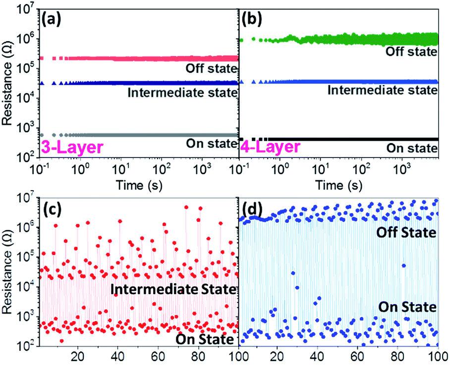 | ||
| Fig. 5 Retention tests of (a) sandwiched layered and (b) alternative 4 layered thin film; endurance tests of the 4-layer between (c) ON/intermediate States and (d) ON/OFF States. | ||
In addition, to understand the mechanism of resistive switching in the multi-layer structure, the cell size effect has been analyzed on the 4-layer sample with different top electrode diameters of 250 μm and 150 μm. The retention tests are provided in ESI Fig. S-3.† The resistance levels of 150 μm are only slightly higher than that of 250 μm, suggesting that the resistive switching is mainly because of local phenomenon.29 The temperature dependence of resistance level were tested by heating up the 4-layer on a hot plate from 20 °C to 100 °C. Compared to the change in ON state, there is an obvious decrease in the resistance of OFF states and a slight decrease in that of intermediate states as shown in ESI Fig. S-4.† Such results agrees with previous report, which was ascribed to a typical semiconductor behavior with temperature dependence.30
Conclusion
In conclusion, thin films composed of repetition un-doped and doped SnO2 layers were fabricated. Such structure demonstrated stable multiple resistance states controlled by Mn interstitials migration in the presence of applied electric field. For this structure, the formation and elimination of the Mnint migration pathway can be manipulated by external field to realize more stable intermediate state with over 7200 seconds retention time, low set potential (∼2 V) and higher ON/OFF ratio (over 103). This approach can be potentially extended to other functional materials with cationic or anionic defects to achieve multifunctionalities.Conflicts of interest
There are no conflicts to declare.Acknowledgements
This work was supported by the Australian Research Council Project of FT140100032, DP150103006, and DP140104373.References
- K.-H. Kim, S. Hyun Jo, S. Gaba and W. Lu, Appl. Phys. Lett., 2010, 96, 053106 CrossRef.
- S. Park, J. Noh, M.-L. Choo, A. M. Sheri, M. Chang, Y.-B. Kim, C. J. Kim, M. Jeon, B.-G. Lee and B. H. Lee, Nanotechnology, 2013, 24, 384009 CrossRef PubMed.
- Y. C. Yang, F. Pan, Q. Liu, M. Liu and F. Zeng, Nano Lett., 2009, 9, 1636–1643 CrossRef CAS PubMed.
- R. Waser and M. Aono, Nat. Mater., 2007, 6, 833–840 CrossRef CAS PubMed.
- G. Bersuker, D. Gilmer, D. Veksler, P. Kirsch, L. Vandelli, A. Padovani, L. Larcher, K. McKenna, A. Shluger and V. Iglesias, J. Appl. Phys., 2011, 110, 124518 CrossRef.
- M.-J. Park and J.-S. Lee, RSC Adv., 2017, 7, 21045–21049 RSC.
- M. M. Rehman, G. U. Siddiqui, J. Z. Gul, S.-W. Kim, J. H. Lim and K. H. Choi, Sci. Rep., 2016, 6, 36195 CrossRef CAS PubMed.
- S. Li, H. Zeng, S. Zhang and X. Wei, Appl. Phys. Lett., 2013, 102, 153506 CrossRef.
- J. J. Yang, M. D. Pickett, X. Li, D. A. Ohlberg, D. R. Stewart and R. S. Williams, Nat. Nanotechnol., 2008, 3, 429–433 CrossRef CAS PubMed.
- S. H. Jo, K.-H. Kim and W. Lu, Nano Lett., 2009, 9, 870–874 CrossRef CAS PubMed.
- M. Liu, Z. Abid, W. Wang, X. He, Q. Liu and W. Guan, Appl. Phys. Lett., 2009, 94, 233106 CrossRef.
- Y. Wang, Q. Liu, S. Long, W. Wang, Q. Wang, M. Zhang, S. Zhang, Y. Li, Q. Zuo and J. Yang, Nanotechnology, 2009, 21, 045202 CrossRef PubMed.
- D.-H. Lim, G.-Y. Kim, J.-H. Song, K.-S. Jeong, D.-C. Kim, S.-W. Nam, M.-H. Cho and T.-G. Lee, RSC Adv., 2015, 5, 221–230 RSC.
- N. D. Mathur, Nature, 2008, 455, E13 CrossRef CAS.
- Q. Liu, W. Guan, S. Long, R. Jia, M. Liu and J. Chen, Appl. Phys. Lett., 2008, 92, 012117 CrossRef.
- C. Moreno, C. Munuera, S. Valencia, F. Kronast, X. Obradors and C. Ocal, Nano Lett., 2010, 10, 3828–3835 CrossRef CAS PubMed.
- H.-S. PhilipáWong, Nanoscale, 2014, 6, 5698–5702 RSC.
- S. Yu, B. Gao, Z. Fang, H. Yu, J. Kang and H. S. P. Wong, Adv. Mater., 2013, 25, 1774–1779 CrossRef CAS PubMed.
- Y.-F. Chang, B. Fowler, Y.-C. Chen, F. Zhou, C.-H. Pan, T.-C. Chang and J. C. Lee, Sci. Rep., 2016, 6, 21268 CrossRef CAS PubMed.
- P.-H. Liu, C.-C. Lin, A. Manekkathodi and L.-J. Chen, Nano Energy, 2015, 15, 362–368 CrossRef CAS.
- S. Almeida, B. Aguirre, N. Marquez, J. McClure and D. Zubia, Integr. Ferroelectr., 2011, 126, 117–124 CrossRef CAS.
- C. Nieh, M. Lu, T. Weng and Y. Chen, Appl. Phys. Lett., 2014, 104, 213501 CrossRef.
- F. Trani, M. Causà, D. Ninno, G. Cantele and V. Barone, Phys. Rev. B: Condens. Matter Mater. Phys., 2008, 77, 245410 CrossRef.
- X. Wu, Z. Xu, F. Zhao, X. Xu, B. Liu, T. Sun, S. Liu, W. Zhao and Z. Ma, J. Alloys Compd., 2014, 602, 175–179 CrossRef CAS.
- Z. Xu, A. Younis, D. Chu, J. Yi and S. Li, Phys. Chem. Chem. Phys., 2017 Search PubMed , Manuscript under review.
- F. Ghodsi and J. Mazloom, Appl. Phys. A, 2012, 108, 693–700 CrossRef CAS.
- H. J. Kim, Y.-J. Baek, Y. J. Choi, C. J. Kang, H. H. Lee, H.-M. Kim, K.-B. Kim and T.-S. Yoon, RSC Adv., 2013, 3, 20978–20983 RSC.
- K. Park and J.-S. Lee, RSC Adv., 2016, 6, 21736–21741 RSC.
- A. Sawa, Mater. Today, 2008, 11, 28–36 CrossRef CAS.
- P. Feng, C. Chao, Z.-S. Wang, Y.-C. Yang, Y. Jing and Z. Fei, Prog. Nat. Sci.: Mater. Int., 2010, 20, 1–15 CrossRef.
Footnote |
| † Electronic supplementary information (ESI) available. See DOI: 10.1039/c7ra11681k |
| This journal is © The Royal Society of Chemistry 2017 |