
 Open Access Article
 This Open Access Article is licensed under a
 Creative Commons Attribution 3.0 Unported Licence
Samarium doped Sn15Sb85: a promising material for phase change memory applications
Hua Zou *a,
Liangjun Zhaia,
Yifeng Hu*a,
Xiaoqin Zhua,
Haipeng Youa,
Jianhao Zhanga,
Sannian Songb and
Zhitang Songb
*a,
Liangjun Zhaia,
Yifeng Hu*a,
Xiaoqin Zhua,
Haipeng Youa,
Jianhao Zhanga,
Sannian Songb and
Zhitang Songb
aSchool of Mathematics and Physics, Jiangsu University of Technology, Changzhou, 213001, P. R. China. E-mail: zouhua@jsut.edu.cn; hyf@jsut.edu.cn
bState Key Laboratory of Functional Materials for Informatics, Shanghai Institute of Micro-system and Information Technology, Chinese Academy of Sciences, Shanghai 200050, China
First published on 11th December 2017
Abstract
The thermal stability of phase change films is a key parameter in phase change memory (PCM) applications. Here, we find that the Sm doped Sn15Sb85 films have a higher crystallization temperature and a better data retention ability in comparison with those of pure amorphous SnSb films, revealing a potential candidate for PCM applications. In addition, it demonstrated that the Sm doping was also propitious to reduce the power consumption and decrease the change of roughness in the crystallization process. Finally, the data storage capability of the Sm0.015(Sn15Sb85)0.985-based PCM cell was obtained with a reversible phase change process between high and low resistance states.
1 Introduction
In the last few years, chalcogenide-based phase change memory (PCM) has attracted intensive attention as a next-generation substitute for non-volatile random access memory.1 Compared with other novel solid-state memories, PCM possesses its conspicuous advantages, including fast access time, high density, low power consumption, excellent scalability and high cycle numbers.2 So far, the most known and used chalcogenide material is Ge2Sb2Te5 ternary alloys (GST) due to their exceptional characteristics such as good scalability and high phase change speed.3 However, it is highly challenging to prepare chalcogenide phase change films with improved properties.4Recently, Sb-based materials, such as Sn–Sb,5 Ge–Sb,6 Sb–Te7 and Ga–Sb,8 have been considered as promising candidates for PCM applications because of their ultra-high phase speed. Feng Rao et al. reported that a Sn12Sb88-based cell is able to show quicker set operation speed, better data retention ability, and lower reset power consumption than the cell based on the GST.5 Yegang Lu et al. have proved that the SET/RESET process of the devices based on Ga14Sb86 alloys could be operated by a 20 ns pulse.8 Feng Rao et al. demonstrated that the Sc0.2Sb2Te5 compound allows an ultrafast writing speed of only 700 picoseconds compared with a conventional PCM device.9 However, a material with fast crystallization speed is generally not stable. In order to solve this contradiction, doping is equally significant for improving the performance of Sb-based alloys.10 Recently, N,11 O,12 Al,13 W,14 Si15 and SiC16 were demonstrated as effective elements for doping.
Rare earth element (RE) is one of a set of seventeen chemical elements in the periodic table, which has been worldwide used in industrial application, even used in fertilizer, feed additives.17 In phase change memory, we have reported that the Er can significantly improve the performance of Sb-based alloys.18–21 Unfortunately, very little work has been done to elucidate the effect of rare element on the phase change properties. It is urgent to explore the effect and their mechanisms in phase change materials by doping with other rare earth, such as Sm, Pr and etc. In this work, the objective is to systematically investigate the effect of Sm doping on phase change properties in SnSb alloys. The thermal stability, crystal structure, and device were studies in details.
2 Experiments
The Sm doped Sn15Sb85 thin films of Smx(Sn15Sb85)1−x (0 ≤ x ≤ 0.020) used for our study were made by Magnetron Co-sputtering Sm and Sn15Sb85 targets onto square SiO2/Si (100) wafers at room temperature. The purity of Sm and Sn15Sb85 targets was 99.999%. The base pressure in the deposition chamber was 2 × 10⁻⁴ Pa. Sputtering was performed under the Ar gas pressure of 0.3 Pa, the flow of 30 sccm. The thin film thickness was set to 50 nm through controlling deposition time of Sn15Sb85. The doped Sm content was altered by adjust the Sm sputtering power, while the sputtering power of Sn15Sb85 was maintained at 30 W. The deposition rate was 2.6 nm s−1. To ensure the uniformity of deposition, the substrate holder was rotated at an autorotation speed of 20 rpm.The amorphous to crystalline transition was investigated by in situ temperature–dependent resistance (R–T) measurement using a TP 95 temperature controller (Linkam Scientific Instruments Ltd. Surrey, UK) under Ar atmosphere. The crystalline structures of the films were analyzed by X-ray diffraction (XRD, PANalytical, X’PERT Powder). In order to assess the chemical bonding states of Sm doped Sn15Sb85 film, the X-ray photoelectron spectroscopy (XPS, Thermo Scientific, K-Alpha) was carried out. The surface morphology of the films was examined by atomic force microcopy (AFM, FM-Nanoview 1000). The PCM devices based on the Sm0.015(Sn15Sb85)0.985 thin film with a tungsten heating electrode of 260 nm diameter were fabricated by 0.18 μm CMOS technology. Between the Sm0.015(Sn15Sb85)0.985 film and the top electrode, a 20 nm thick TiN film was deposited by direct current magnetron sputtering. Current–voltage (I–V) and resistance–voltage (R–V) were conducted using a Keithley 2400 semiconductor parameter analyzer and an Agilent 81104A programmable pulse generator.
3 Results and discussion
To analyze crystallization temperature (Tc) of Sm doped Sn15Sb85 films, the sheet resistance as a function of temperature is shown at a heating rate of 20 °C in Fig. 1(a). With increasing the Sm doping, the results show the Tc increase significantly. In general, the Tc is defined by the derivative of the resistance with respect to temperature (dR/dT).22 In Fig. 1(b), it can be seen that as Sm content increases, the Tc increase from 201 °C of pure Sn15Sb85 to 214, 226, 242 °C for Sm0.005(Sn15Sb85)0.995, Sm0.010(Sn15Sb85)0.990 and Sm0.015(Sn15Sb85)0.985. It obviously indicates a better thermal stability of amorphous phase by Sm doping, which will be propitious to achieve more thermal stable PCM cells. In a previous paper,19 we confirmed that the Er dopants (the content of ∼2.4%) can increase the Tc of 43 °C compared with pure Sn15Sb85. In this work, it shows that the Sm dopants (∼1.5%) can increase the Tc of 41 °C, which indicates that Sm dopants would have much remarkable influence. Fig. 1(a) also shows that the amorphous and crystalline resistance increases with increasing the Sm content, which reveals much less pulse current to realize the phase transition by Joule heating. | ||
| Fig. 1 (a) Sheet resistance of pure Sn15Sb85 and Sm doped Sn15Sb85 as a function of the temperature with a heating rate of 20 °C min−1. (b) The first derivative of R–T curve of the pure and Sm doped Sn15Sb85 films. | ||
In order to further estimate the retention of amorphous Sm doped Sn15Sb85 films, the crystallization of isothermal annealing at different temperature was studied as shown in Fig. 2. It observes that the initial period remains unchanged due to the nucleation process of crystalline grains. After the process, the grains of the film grow rapidly meaning the sudden decrease of the resistance. For directly expressing the retention, it usually can be measured by the Arrhenius equation: 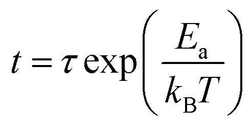 , where t, τ, kB and T are the failure time, pre-exponential factor depending on the materials' properties, Boltzmann constant and absolute temperature.23 The failure time is defined by the time when the resistance decreases to its half value. As shown in the inset of Fig. 2, the Ea and temperature for 10 years archival life (Tten) can be determined by the linear fit of amorphous resistance as a function of 1/kBT. It can be shown that the Ea is 3.36, 3.23, 4.84, 4.88 eV and the Tten is 119, 132, 161, 174 °C, respectively. Thus, the increase of Ea and Tten indicates the PCM cells based on Sm doped Sn15Sb85 films can store information much longer than the pure Sn15Sb85 alloys. Compared with Er0.018(Sn15Sb85)0.082 of Tten (∼149 °C), the Sm0.015(Sn15Sb85)0.085 possess much higher Tten (∼175 °C). The superior enhancement of thermal stability may ascribe to the much bigger Sm3+ ion compared with Er3+ ion.24 In addition, to compete with NOR-Flash memory, the Tten for PCM cells should be higher than 125 °C.25 In this perspective, the Sm doped Sn15Sb85 alloys with high Tten are promising candidate for PCM application.
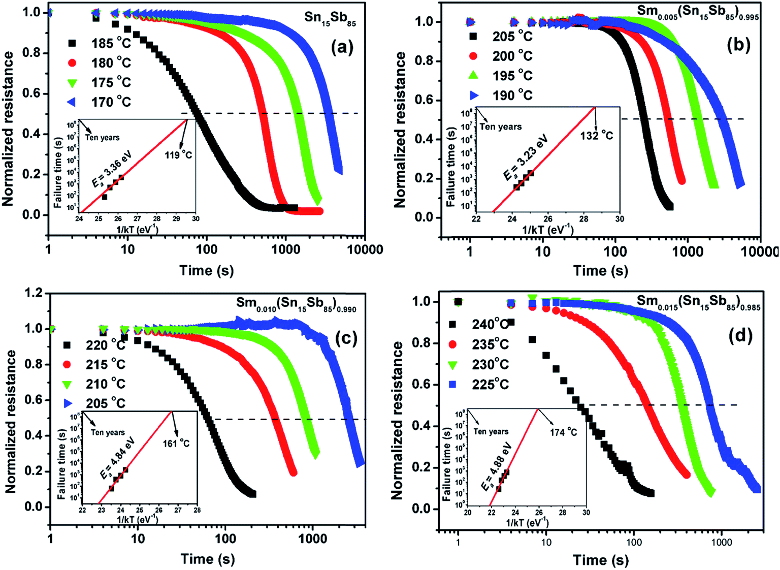 | ||
| Fig. 2 Normalized resistance of (a) Sn15Sb85, (b) Sm0.005(Sn15Sb85)0.995, (c) Sm0.010(Sn15Sb85)0.990, (d) Sm0.015(Sn15Sb85)0.985 thin film as a function of time. The inset is the plots of failure times as a function of reciprocal temperature. | ||
The crystalline structure of Sm doped Sn15Sb85 films can be verified by XRD. But it is difficult to investigate the structure of 50 nm-thick film because of its low mass and small scale. Thus we choose the typical XRD pattern of 300 nm-thick Sn15Sb85 and Sm doped Sn15Sb85 to investigate the phase structure.26 Fig. 3(a) shows the rhombohedra phase of Sb only exists after annealing at 280 °C, revealing only the amorphous to rhombohedra phase process. More importantly, the intensity for (110) planes decrease significantly by increasing the Sm dopants, meaning the reversible phase change can be realized more difficult by Sm doping, which may be helpful in enhancing the thermal stability. Fig. 3(b) shows the evolution of the XRD pattern as the function of the heating temperature. For the as deposited film, there is no peak in the XRD pattern, meaning the amorphous structure. Then, it is apparent that the films crystallize into the rhombohedra phase when the annealing temperature up to 210 °C. In addition, the intensity of (110) plane increases with increasing the annealing temperature, indicating the increase of grain size. These results are consistent with those reports for Er doped SnSb films.
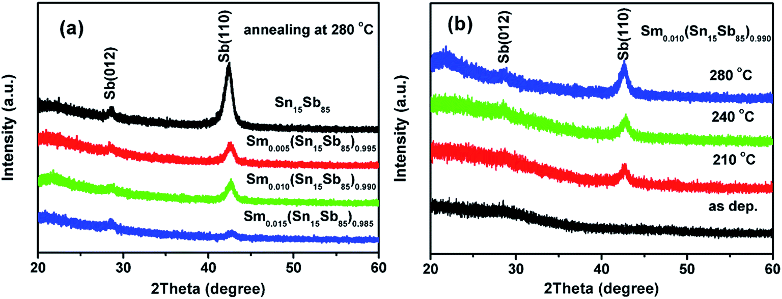 | ||
| Fig. 3 (a) XRD pattern of annealed Sm doped Sn15Sb85 and pure Sn15Sb85 films at 280 °C for 10 min; (b) XRD pattern of Sm0.010(Sn15Sb85)0.990 films annealed at different temperature for 10 min in Ar atmosphere. | ||
In a previous work, we reported that the improvement of performance of SnSb alloys by Er doping was due to the existence of Er–Sb bonding.19 To explore the change of chemical bonding states of Sb and Sn atoms, the XPS spectra were measured as shown in Fig. 4. After Sm doping, Fig. 4(a) shows there is the chemical shift of 0.07 eV based on Sb 3d core-level. In addition, the peak of Sn–Sb bonds also shift to higher energies by Sm doping. This result obviously means that the Sm–Sb bond existence in Sm doped SnSb alloy by substitution of Sb–Sb and Sn–Sb bond. Fig. 4(b) indicates that the peak of Sn 3d shift to high energies by Sm doping, which reveals the formation of Sn–Sm bond in films. This result is also consistent with the Er doped SnSb alloys. Thus, the formation of Sm–Sb and Sm–Sb may be the key reason for improving the performance of the materials.
 | ||
| Fig. 4 (a) High resolution Sb 3d and (b) high resolution Sn 3d XPS spectra of the Sn15Sb85 and Sm0.015(Sn15Sb85)0.985 thin films annealed at 280 °C for 10 min. | ||
In general, the electrical properties depend on not only the phase change materials but also the contact quality between the materials and the electrode. Thus, minimizing the surface roughness of phase change materials is essential for PCM device performance, which can maintain good contact quality. Fig. 5 shows the same scale (4 μm × 4 μm) topographic images of as-deposited and annealed at 280 °C Sn15Sb85 and Sm0.015(Sn15Sb85)0.985 thin films. As seen from the Fig. 5, the root mean square (RMS) roughness calculated from the AFM images. Firstly, it indicates the grain and roughness of Sm doped Sn15Sb85 film are relatively very small. In addition, the crystallization leads to an increase in grain size and roughness. More importantly, these results reveal that by Sm doping, the change of roughness is smaller than pure Sn15Sb85. In view of this, the Sm doping will be propitious to make high performance PCM devices.
 | ||
| Fig. 5 AFM images (a) as-deposition and (b) annealed at 280 of pure Sn15Sb85 for 10 min; AFM images of (c) as-deposition and (d) annealed at 280 °C of Sm0.015(Sn15Sb85)0.985 for 10 min. | ||
At last, T-shaped PCM cells based on Sm0.015(Sn15Sb85)0.985 alloys fabricated by 0.18 μm CMOS technology was utilized to test and verify their electrically induced phase change abilities. The inset of Fig. 6 shows the schematic diagram of the PCM cells. Fig. 6(a) shows the DC current–voltage (I–V) curve, which has a clear threshold switching behaviour at a threshold voltage, Vth. The Vth is 1.5 V based on the Sm doped Sn15Sb85 PCM device, which is almost the same as that of Sn12Sb88 based PCM device (∼1.6 V).5,8 Fig. 6(b) shows the R–V curves of the device. When the reset threshold voltage (∼2.5 V for 300 ns pulse width), the set state of PCM device (103–104 Ω) can be swiftly transferred to the reset state (105–106 Ω). This results also indicate the device based on the Sm doped Sn15Sb85 have the same properties in the PCM cell.
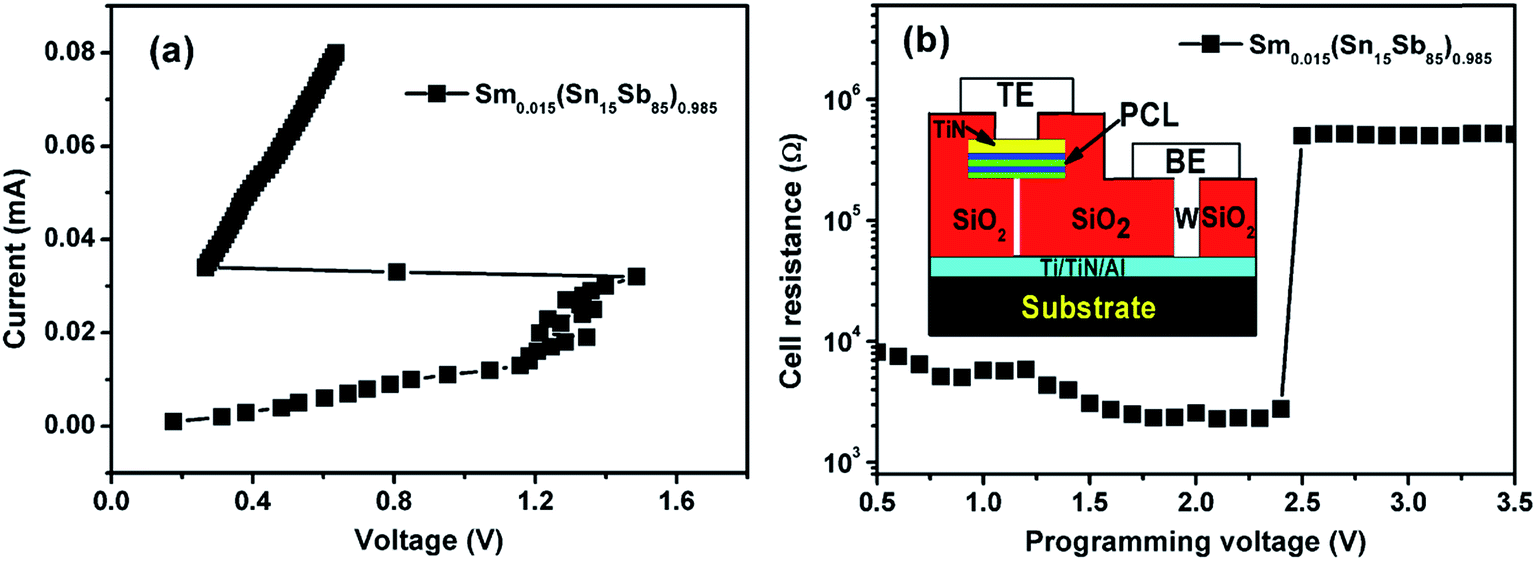 | ||
| Fig. 6 (a) I–V and (b) R–V curves of PCM cell based on Sm0.015(Sn15Sb85)0.985 materials. Inset in (b) shows schematic diagram of cross-sectional cell structure. | ||
4 Conclusions
In summary, we have systematically demonstrated the effect of Sm doping on phase change performance in Sn15Sb85 alloys. The Sm doped Sn15Sb85 films have the higher Tc, Ea and Tten, which ensure much better data retention for PCM application. The amorphous and crystallization resistance are proved to be larger than of pure SnSb alloys, which will reduce the power consumption for PCM cell. Compared with pure SnSb system, the XRD measurement certified that the Sm dopant don't change the phase structure and improve the thermal stability. The XPS tests prove the existence of Sb–Sm and Sn–Sm bond, which give rise to performance. The AFM tests prove that the Sm doped thin film have much lower change of roughness in crystallization process. The reversible phase change between set and reset state is obtained based on the Sm doped Sn15Sb85 PCM devices. Therefore, the Sm doped SnSb alloys are attractive candidates for PCM application. In addition, to clearly confirm rare earth doping effect on electrical properties, such as Pr, Ce and etc., further works should carefully check the phase change properties and the device characteristics.Conflicts of interest
There are no conflicts to declare.Acknowledgements
The work was supported by the National Natural Science Foundation of China (No. 11704161, 11774438), Natural Science Foundation of Jiangsu Province (No. BK20151172, BK20170309), Changzhou Sci&Tech Program (No. CJ20160028), and sponsored by Qing Lan Project.References
- M. Wuttig, Nat. Mater., 2005, 4, 265–266 CrossRef CAS PubMed.
- X. Zhou, J. Kalikka, X. Ji, L. Wu, Z. Song and R. E. Simpson, Adv. Mater., 2016, 28, 3007–3016 CrossRef CAS PubMed.
- S. Raoux and D. Ielmini, Chem. Rev., 2009, 110, 240–267 CrossRef PubMed.
- D. Lencer, M. Salinga, B. Grabowski, T. Hickel, J. Neugebauer and M. Wuttig, Nat. Mater., 2008, 7, 972–977 CrossRef CAS PubMed.
- F. Rao, Z. Song, K. Ren, X. Li, L. Wu, W. Xi and B. Liu, Appl. Phys. Lett., 2009, 95, 032105 CrossRef.
- G. Eising, T. Van Damme and B. J. Kooi, Cryst. Growth Des., 2014, 14, 3392–3397 CAS.
- G. Wang, Y. Chen, X. Shen, Y. Lu, S. Dai, Q. Nie and T. Xu, J. Appl. Phys., 2015, 117, 045303 CrossRef.
- Y. Lu, S. Song, Z. Song and B. Liu, J. Appl. Phys., 2011, 109, 064503 CrossRef.
- F. Rao, K. Ding, Y. Zhou, Y. Zheng, M. Xia, S. Lv, Z. Song, S. Feng, I. Ronneberger, R. Mazzarello, W. Zhang and E. Ma, Science, 2017, eaao3212 CrossRef PubMed.
- T. H. Lee, D. Loke and S. R. Elliott, Adv. Mater., 2015, 27, 5477–5483 CrossRef CAS PubMed.
- X. Q. Zhu, Y. F. Hu, L. Yuan, Y. X. Sui, J. Z. Xue, D. H. Shen, J. H. Zhang, S. N. Song and Z. T. Song, J. Electron. Mater., 2015, 44, 3322–3326 CrossRef CAS.
- R. Golovchak, Y. G. Choi, S. Kozyukhin, Y. Chigirinsky, A. Kovalskiy, P. Xiong-Skiba, J. Trimble, R. Pafchek and H. Jain, Appl. Surf. Sci., 2015, 332, 533–541 CrossRef CAS.
- Y. Hu, X. Zhu, H. Zou, Y. Lu, J. Xue, Y. Sui, W. Wu, L. Yuan, S. Song and Z. Song, J. Mater. Sci.: Mater. Electron., 2015, 26, 7757–7762 CrossRef CAS.
- R. Kun, X. Mengjiao, R. Feng, S. Zhitang, D. Keyuan, J. Xinglong, W. Liangcai, L. Bo and F. Songlin, Appl. Phys. Lett., 2014, 104, 173102–173105 CrossRef.
- L. Tong, L. Xu, Y. Jiang, F. Yang, L. Geng, J. Xu, W. Su, Z. Ma and K. Chen, J. Non-Cryst. Solids, 2012, 358(17), 2402–2404 CrossRef CAS.
- T. Guo, S. Song, L. Li, X. Ji, C. Li, C. Xu, L. Shen, Y. Xue, B. Liu, Z. Song, M. Qi and S. Feng, Scr. Mater., 2017, 129, 56–60 CrossRef CAS.
- H. Zou, X. Wang, Y. Hu, X. Zhu, Y. Sui and Z. Song, AIP Adv., 2014, 4, 127157 CrossRef.
- H. Zou, X. Zhu, Y. Hu, Y. Sui, W. Wu, J. Xue, L. Zheng and Z. Song, CrystEngComm, 2016, 18, 6365–6369 RSC.
- H. Zou, X. Zhu, Y. Hu, Y. Sui, Y. Sun, J. Zhang, L. Zheng and Z. Song, J. Appl. Phys., 2016, 120, 245303 CrossRef.
- H. Zou, Y. Hu, X. Zhu and Z. Song, RSC Adv., 2017, 7, 31110–31114 RSC.
- H. Zou, Y. Hu, X. Zhu, Y. Sun, L. Zheng, Y. Sui, S. Wu and Z. Song, J. Mater. Sci., 2017, 52, 5216–5222 CrossRef CAS.
- L. Li, S. Song, Z. Zhang, L. Chen, Z. Song, S. Lv, B. Liu and T. Guo, Solid-State Electron., 2016, 120, 52–55 CrossRef CAS.
- X. Ji, L. Wu, W. Zhou, M. Zhu, F. Rao, Z. Song, L. Cao and S. Feng, Appl. Phys. Lett., 2015, 106, 023118 CrossRef.
- R. Shannon, Acta Crystallogr., Sect. A: Cryst. Phys., Diffr., Theor. Gen. Crystallogr., 1976, 32, 751–767 CrossRef.
- T. Morikawa, K. Kurotsuchi, Y. Fujisaki, Y. Matsui and N. Takaura, Jpn. J. Appl. Phys., 2012, 51, 031201 Search PubMed.
- H. Zou, X. Zhu, Y. Hu, Y. Sui, L. Zheng, W. Wu, L. Zhai, J. Xue and Z. Song, J. Mater. Sci.: Mater. Electron., 2017, 28, 3806–3811 CrossRef CAS.
| This journal is © The Royal Society of Chemistry 2017 |