
 Open Access Article
 This Open Access Article is licensed under a
 Creative Commons Attribution 3.0 Unported Licence
Multilayer core–shell MoS2/CdS nanorods with very high photocatalytic activity for hydrogen production under visible-light excitation and investigation of the photocatalytic mechanism by femtosecond transient absorption spectroscopy†
Zhiping Yan,
Lili Du * and
David Lee Phillips*
* and
David Lee Phillips*
Department of Chemistry, The University of Hong Kong, Hong Kong S.A.R., China. E-mail: phillips@hku.hk; ailleen@hku.hk
First published on 12th December 2017
Abstract
Understanding the structural features and the dynamics and properties of charge carriers in photocatalysts is critical to develop them for practical applications. Photocatalytic H2 production on molybdenum sulfide/cadmium sulfide (MoS2/CdS) nanorods in the presence of lactic acid under visible light (λ > 420 nm) was investigated. The optimized MoS2/CdS photocatalysts with 1.52 wt% MoS2 showed the highest rate of 154.748 μmol h−1 mg−1, which is 5 times faster than that of bare CdS nanorods. Experimental results from HR-TEM, UV-vis, and photoelectrochemical measurements suggest that an intimate contact interface, extended light response range, effective separation of the photogenerated charge carriers and high photocurrent density on the MoS2 modification contributed to the photocatalytic enhancement of the MoS2/CdS photocatalysts. Electrochemical measurements indicate that MoS2 is an efficient H2 evolution co-catalyst, which is attributed to the promotion of the photocatalytic activity. Femtosecond transient absorption (fs-TA) spectroscopy was performed to investigate the dynamics of the charge carriers that led to hydrogen production by these composites. The results reveal that the enhanced hole trapping process and effective electrons transfer (within 14.8 ps) from CdS to MoS2 in MoS2/CdS composites can promote their photocatalytic activity dramatically.
Introduction
Photocatalytic H2 production from water has attracted great attention since it can contribute significantly as an environmentally friendly energy source. An enormous amount of work has been done by researchers aimed at improving the efficiency of H2 production from a range of different kinds of photocatalysts.1,2 In particular, much effort has been given toward the development of visible-light-responsive photocatalysts, such as those based on CdS,3,4 ZnS,5,6 Znln2S4 (ref. 7 and 8) and Cu2S9 materials that have been synthesized and demonstrated to be able to produce H2.Among various candidates for photocatalysts to produce H2, cadmium sulfide (CdS), as a narrow direct band-gap semiconductor (2.4 eV), has been regarded as a potential semiconductor due to its effective absorption of sunlight and having a suitable conduction band edge for the HER (hydrogen evolution reaction).10 However, problems such as the fast recombination of the photogenerated charge carriers and photocorrosion under visible-light irradiation limit the potential application of CdS in photocatalysis applications.11 In addition to the semiconductor materials, surface modification of photocatalysts with co-catalysts is also crucial for photocatalytic H2 production reactions, because the co-catalysts can promote the separation of photoexcited electrons and holes. Moreover, they can offer low activation energy for HER and may often serve as the active sites for H2 generation.12–14 Platinum (Pt), a well-known co-catalyst for photocatalytic hydrogen production, is too expensive and rare to be suitable for this kind of application on a large scale.15,16
The multi-layer MoS2 has an indirect band gap of about 1.3 eV while its monolayer form with a direct energy gap of 1.8 eV. So, layered molybdenum sulfide (MoS2) may be coupled with CdS and can be an ideal candidate due to its appropriate band edge, large surface area, high thermal stability and electrostatic integrity. In addition, a p–n junction has been proposed to be formed between MoS2 and CdS, because MoS2 is considered to be a p-type semiconductor. Lee and coworkers first synthesized sheet-like MoS2 to modify CdS QDs.17 Many studies demonstrated that layered MoS2 can significantly enhance photocatalytic hydrogen production when it is loaded on the surface of CdS.18,19 Liu and co-workers constructed MoS2 layer/CdS nanoparticles as photocatalysts and found that the energy of MoS2 and CdS are well-matched for hole and electron transport.20 The high activity of this photocatalyst has been shown for visible light photoelectrocatalytic activity.
In this work, MoS2 was found to be an efficient co-catalyst for CdS nanorods in the photocatalytic H2 production reaction using a lactic acid solution as the sacrificial agent under visible light irradiation. This is a good attempt to use MoS2 nanosheets to modify nanorod-like CdS to form an unclosed integrated core–shell structure. The photocatalysts were characterized by powder X-ray diffraction (XRD), UV-visible diffuse reflectance spectroscopy (UV-vis), X-ray photoelectron spectroscopy (XPS), and femtosecond transient absorption (fs-TA) spectroscopy. We demonstrate that MoS2 loading can greatly enhance the photocatalytic activity of CdS nanorods, and examine the transportation of photogenerated carriers in MoS2/CdS using fs-TA. In our research, the composites show an inspiring photocatalytic efficiency compared with some similar work,21–23 the special multilayer core–shell structure of the sample is considered to provide more active sites which could promote the photocatalytic activity. Moreover, fs-TA performed to illuminate the photo-induced electron transportation in these heterojunction structures is also a novel characterization in this system. We believe this work will play a meaningful role in the development of heterogeneous photocatalysts.
Experimental
Materials and synthesis of the photocatalyst
All chemicals, including ethylenediamine (C2H4(NH2)2, 99.0%), sodium sulfide (Na2S, 98.0%), sodium sulfite (Na2SO3, 97.0%), cadmium chloride (CdCl2·2.5H2O, 99.0%), thiourea (NH2CSNH2, 99.0%), sodium molybdate (Na2MoO4, 99.0%), sodium sulfate (Na2SO4, 99.0%), lactic acid, and ethanol (99.7%), were all commercially available (Aldrich or Acros) and used without further purification. | ||
| Scheme 1 Schematic illustration for the process of CdS nanorods being modified by MoS2 nanosheets. | ||
Characterization
The morphology of the samples was characterized using a SIRION200 Schottky field emission scanning electron microscope (SFE-SEM). High resolution transmission electron microscopy (HR-TEM) images were collected on a JEM-2010 electron microscope, operated at an acceleration voltage of 200 kV. X-ray diffraction (XRD) patterns, obtained on a D/max-TTR III X-ray diffraction with Cu Kα radiation at a scan rate of 5° min−1 from 10° to 70° in 2θ, were used to characterize the crystalline structure and lattice phases of the samples. X-ray photoelectron spectroscopy (XPS) measurement was performed on an ESCALAB 250 X-ray photoelectron spectrometer. Ultraviolet-visible diffuse reflectance spectra were recorded on a UV-visible spectrophotometer (SOLID 3700 UV-vis spectrometer). Inductively coupled plasma-atomic emission spectroscopy (ICP-AES) results were measured by an Optima 7300 DV.The fs-TA experiments were done employing an experimental setup and methods detailed previously26,27 and only a brief description is provided here. A regenerative amplified Ti:sapphire laser system with an automated data acquisition system were used to conduct the femtosecond transient absorption (fs-TA) spectroscopy experiments, in which the amplifier was seeded with the 120 fs laser pulses from an oscillator laser system. A white-light continuum (350–800 nm) in a CaF2 crystal was generated by the laser probe pulse, which used ∼5% of the amplified 800 nm laser pulses. Then this probe beam was divided into two separate beams before traversing the sample, one goes through the sample, the other is directed going into a reference spectrometer to monitor the fluctuations in the probe beam intensity. For the present experiments, the sample solutions were excited by a 400 nm pump beam (the second harmonic of the fundamental 800 nm from the regenerative amplifier). The 1 mL sample mixed solution (lactic acid/water = 1![[thin space (1/6-em)]](https://www.rsc.org/images/entities/char_2009.gif) :9) were studied in a 2 mm path-length cuvette throughout the data acquisition.
:9) were studied in a 2 mm path-length cuvette throughout the data acquisition.
Photocurrent measurements were performed on a CHI 602E electrochemistry potentiostat. In this three-electrode electrochemical cell, Ag/AgCl and Pt wire worked as the reference electrode, and counter electrode. Irradiation proceeded by a 300 W xenon lamp with a cut-off filter (λ > 420 nm). Sodium sulfate (Na2SO4, 0.5 M) solution was used as the electrolyte. The preparation of working electrode was as follows: dropping the suspensions (15 μL) made of CdS, or MoS2/CdS (the concentration of MoS2/CdS, or CdS is 50 g L−1) onto a 2 × 1 cm indium tin oxide (ITO) plate using a pipette. The working electrodes were dried at room temperature. The scan rate was 50 mV s−1, and the potential in this manuscript corresponds to Ag/AgCl.
Photocatalytic hydrogen production
The reactor for present photocatalytic hydrogen production reaction is shown in Fig. S1.† Generally, the photocatalytic H2 evolution was carried out with 1 mg of photocatalyst suspend in a 20 mL solution containing 2 mL lactic acid in a Pyrex glass flask. A 300 W Xe-lamp equipped with a 420 nm cut-off filter to provide the visible light irradiations was used as the irradiation source. Before each experiment, the suspension was stirred for 10 min in the dark and purged with nitrogen for 15 min to remove air. Methane served as the internal standard. Hydrogen gas evolution was measured by an on-line gas chromatography equipped with a TCD detector (nitrogen as the carrier gas). The activities of different catalysts were compared by the average rate of H2 evolution in the first 3 h.Results and discussion
The core–shell MoS2/CdS nanorod samples were successfully synthesized by an effective method illustrated in Scheme 1. CdS nanorods were first prepared through the reaction of cadmium chloride and thiourea in ethylenediamine. Then the MoS2 nanosheets formed by MoO42− and NH2CSNH2 was introduced to coat the as-prepared CdS nanorods through a hydrothermal process. XRD was used to identify the crystal structure of the CdS and MoS2/CdS samples (see Fig. 1). The loading weight ratios of MoS2 were measured by ICP-AES. All the samples exhibited similar XRD patterns, which could be indexed to a CdS hexagonal structure (JCPDS no. 65-3414).28 The three diffraction peaks at 24.8, 26.5 and 28.2° can be assigned to the (100), (002), and (101) planes, respectively.4 There were no obvious changes when MoS2 was loaded on the surface of CdS, which indicates that the MoS2 has no influence on the crystalline structure of CdS. The main reason for this phenomenon may be attributed to the low content of MoS2.19,29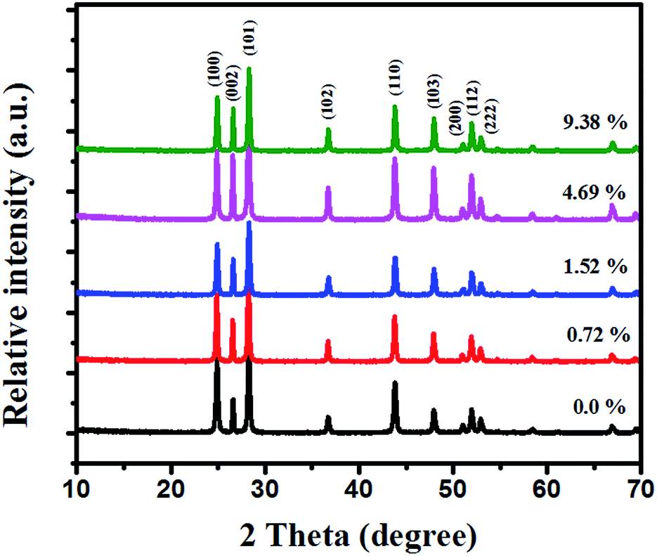 | ||
| Fig. 1 Shown are XRD patterns of pure CdS and MoS2/CdS samples with different weight ratios of MoS2. | ||
Fig. 2a and b shows the SEM images of the as-synthesized samples. SEM observation of MoS2/CdS clearly shows nanorod-like morphology with the lengths of about 1 μm. The structures display good uniformity and the average diameter of the nanorod is 200 nm. To further confirm the interfacial junction between MoS2 and CdS, the MoS2/CdS sample was characterized by HR-TEM. Fig. 2c and d show that the co-catalyst MoS2 with typical layered structure is deposited on the CdS surface.
 | ||
| Fig. 2 (a, b) SEM images of the typical MoS2/CdS (1.52 wt% MoS2). (c, d) HR-TEM images of MoS2/CdS (1.52 wt% MoS2). The inset of (d) gives the histogram of the core–shell structure distribution. | ||
The observed lattice fringes with the spacing of 0.615 nm and 0.357 nm were in good agreement with the interplanar spacings of the (002) and (100) planes of hexagonal MoS2 and CdS, respectively.30,31 The number of the MoS2 slabs deposited on CdS is about 10, and the MoS2 slabs are intimately deposited on the surface of CdS. The intimate contact between MoS2 and CdS favours the formation of junctions between the two semiconductors, and further improves the charge separation.
The chemical composition and electronic structures of MoS2/CdS were analysed typically by XPS. As shown in Fig. 3a, Mo, Cd, S and O were observed on the XPS survey spectra for the MoS2/CdS sample, which confirms the presence of MoS2. The XPS peak for C 1s at 284.8 eV is the characteristic peak, which is used as the standard peak.32 In Fig. 3b, two peaks at 405.3 eV and 412.1 eV are assigned to Cd 3d5/2 and Cd 3d3/2, respectively.33 The Mo 3d doublet peaks at 232.4 eV and 229.4 eV indicate the presence of a + 4 oxidation state of Mo (Fig. 3c).18,34 The S 2p peak was fit by two peaks (Fig. 3d): the peaks at 163.0 eV and 161.9 eV are assigned to S 2p1/2 and S 2p3/2, respectively.35 The XPS results further confirmed the coexistence of MoS2 and CdS in the MoS2/CdS nanorods, which agree well with the HR-TEM images.
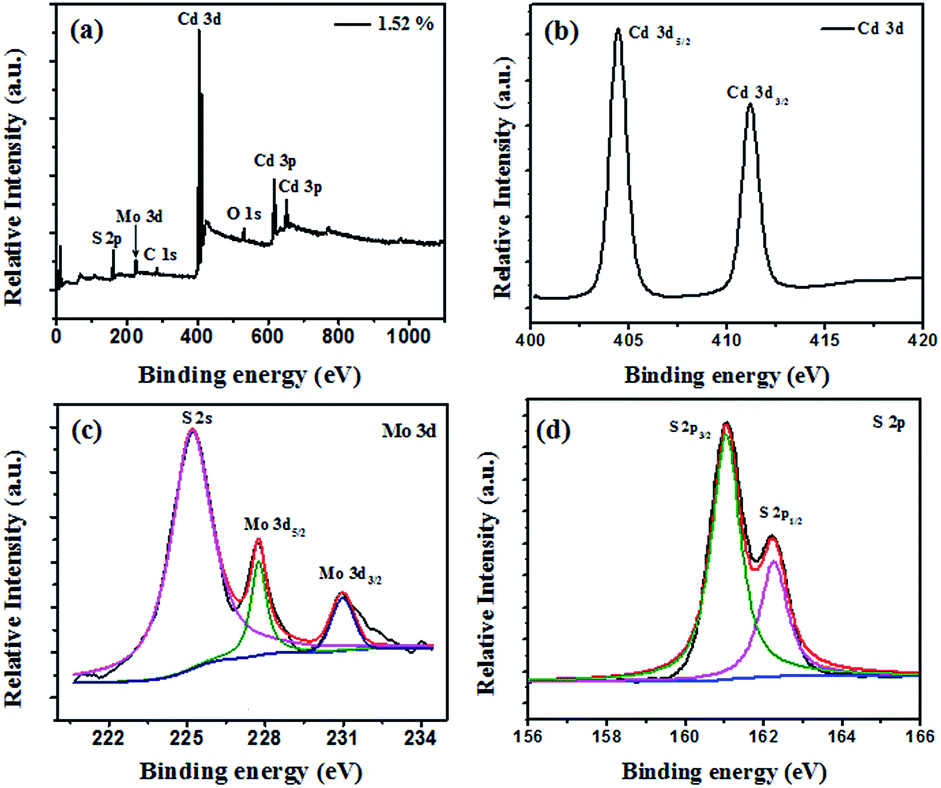 | ||
| Fig. 3 The XPS spectra of (a) full-spectrum scan, (b) Cd 3d, (c) Mo 3d, and (d) S 2p. | ||
The UV-vis diffuse reflectance spectra were used to study the optical absorption properties of the pure CdS and MoS2/CdS samples (Fig. 4). It can be seen that pure CdS can absorb visible light with wavelengths of about 520 nm for its corresponding band gap of 2.4 eV.36 As seen in Fig. S2,† the pure MoS2 showed a wide light absorption among full spectrum range due to its intrinsic narrow band gap of around 1.3 eV and the multilayer structure. Adding MoS2 co-catalysts onto the surface of CdS will increase the absorption of samples under visible light. And with an increasing of the MoS2 content, the absorbance intensity of the composite increased. However, when the ratio of MoS2 reached a certain level in MoS2/CdS samples, the feature of MoS2 began to play a key role which exhibited a red-shift and a less steep absorption edge. These results can be explained by the presence of MoS2, which can extend the visible light absorption region of MoS2/CdS.37,38
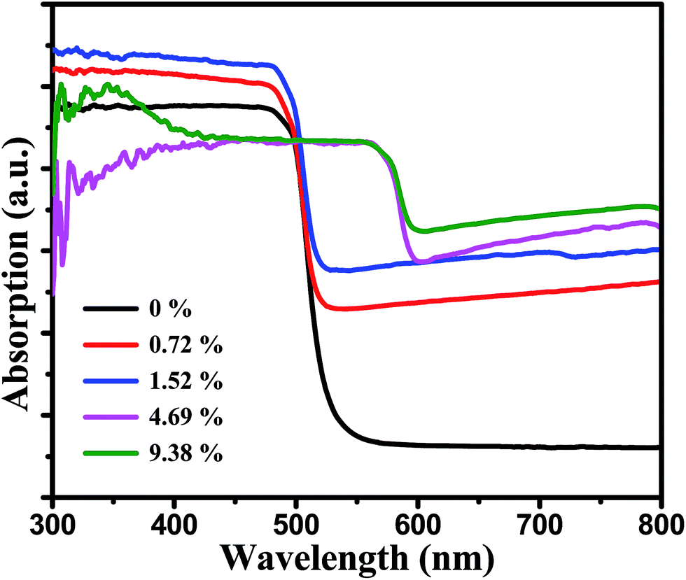 | ||
| Fig. 4 The UV-vis spectra of MoS2/CdS samples with different weight ratios of MoS2. | ||
In order to elucidate the different electron and hole transfer mechanisms between the CdS and the MoS2/CdS systems, femtosecond transient absorption (fs-TA) spectroscopy was employed to illuminate the photo-induced electron transportation in these heterojunction structures. The description for the fs-TA spectroscopy experiments have been mentioned in detail before.39,40 Fig. 5a–c displays the fs-TA spectra of the CdS nanorods in a lactic/H2O = 1:9 mixed solution as a model system to study the competition between the electron transfer, hole trapping and hole transfer processes in the MoS2/CdS heterostructures. As shown in Fig. 5a, the bleach band at 500 nm increased rapidly (within 1 ps) and this is due to the excitation-induced state filling of the lowest-energy 1S(e)-1S3/2(h) transitions of CdS.41 In the later delay times (from 1 ps to 3 ns), only a decreasing of the signal was observed for the bleaching band at 500 nm. Unlike the behavior obtained for the bleaching band at 500 nm, the absorption band at 460 nm performed differently. After 1 ps, the absorption band at 460 showed up and increased in intensity until 18.1 ps and this behavior could be assigned to the trapping process of holes in the surface traps of CdS.42,43 After 18.1 ps, the trapped holes decayed over the next 3 ns. The fitting results are listed in Table 1. After fitting the kinetics at 460 nm by a tri-exponential function in Table S1,† the growth time constant is 8 ps, which can be assigned to the trapping rate of the holes after excitation. The decay of the bands at 460 nm can be attributed to the elimination of the trapped holes by a hole scavenger and/or recombination with the electrons.43 The kinetics at 500 nm were also fit by a tri-exponential function as shown in Table 1 with time constants of 5.7 ps (18%), 51.6 ps (74%) and 1.47 ns (8%). The facile process with the lifetime around 6 ps can be attributed to shallow electron trapping,44 while the slower time constants (51.6 ps and 1.47 ns) indicate the recombination processes of the conduction band electrons with trapped holes and the holes on the valence band, respectively.
 | ||
| Fig. 5 Shown are the fs-TA spectra of CdS nanorods after excitation by 400 nm excitation in a lactic acid/water = 1:9 mixed solution. | ||
| Lifetimes (ps) | CdS | 1.52% MoS2/CdS |
|---|---|---|
| τ1 | 5.7 (18%) | 14.8 (45%) |
| τ2 | 51.6 (74%) | 51.5 (47%) |
| τ3 | 1473 (8%) | 1212 (8%) |
The fs-TA spectra of the 1.52% MoS2/CdS composite are displayed in Fig. 6. Similar with the CdS system, the state filling of the 1S(e)-1S3/2(h) transitions induced a strong bleaching band at 502 nm within 1 ps. The redshifted and broader bleaching band is due to the presence of MoS2, which is consistent with the UV-vis results. Unlike the CdS nanorod, the hole trapping process was observed since 0.6 ps (Fig. 6a) with a growth time constant in 3 ps (see Table S1†) for the 1.52% MoS2/CdS composite, which may result from the interfacial hole trapping process between the CdS and MoS2. The comparison of the difference between the Fig. 5 and 6 data is displayed in Fig. S4.† After normalization of the band at 500 nm, the intensity for the absorption band at 460 nm of the 1.52% MoS2/CdS composite is much higher than the same band for the CdS nanorod, which indicates that the holes are much more easily to be trapped in the 1.52% MoS2/CdS composite after excitation. The enhanced hole trapping process could inhibit the recombination of the electrons and holes, which may lead to the promotion of the photocatalytic activity. On the other hand, as shown in Table 1, after fitting the kinetics at 500 nm for the 1.52% MoS2/CdS composite by a tri-exponential function, the time constants with 14.8 ps (45%), 51.5 ps (47%) and 1.21 ns (8%) were obtained. As pointed by Jones,44 the electron traps were shallow. Therefore, the electron trapping could be inhibited after decoration of MoS2 on the surface of the CdS nanorod. Instead of electron trapping, the electron transfer is supposed to happen from the 1S(e) to the conduction band of the MoS2 with in 14.8 ps.42,45 The slower process (51.5 ps and 1.21 ns) could be due to the recombination processes of the electrons with the trapped holes and the holes on the valence band separately, as discussed above.
 | ||
| Fig. 6 Shown are the fs-TA spectra of 1.52% MoS2/CdS composites after excitation by 400 nm excitation in a lactic acid/water = 1:9 mixed solution. | ||
Therefore, the fs-TA experiment provides us an insight into the photocatalytic process of the 1.52% MoS2/CdS system. In the presence of the MoS2, the enhanced hole trapping process and electron transfer from CdS to MoS2 may illuminate the reason for the efficient H2 evolution activity in the composite system.
The photocatalytic hydrogen evolution on the MoS2/CdS samples were measured by using lactic acid as the sacrificial agent under visible light irradiation. Fig. 7a and b show the time courses of the H2 production of the MoS2/CdS samples with different MoS2 content (0–9.38 wt%). It is clear that MoS2/CdS shows significantly enhanced photocatalytic activity as compared with a pure CdS sample. The rate of H2 production on pure CdS was only 32.690 μmol h−1 mg−1, which was around one fifth that of MoS2/CdS (1.52 wt%). This result may be caused by the poor hole trapping process, electron transfer and fewer active sites in the CdS sample. Moreover, the content of MoS2 had an important influence on the photoactivity of the MoS2/CdS composites. As shown in Fig. 7b, MoS2/CdS with 1.52 wt% MoS2 displayed the optimal H2 evolution rate (154.748 μmol h−1 mg−1) among all the samples examined here. Further increases of the MoS2 content led to a gradual reduction of the photocatalytic hydrogen production rate of MoS2/CdS, and this is probably because there may be too many MoS2 layers loaded that would keep light from the CdS nanorods, which is consistent with the UV-vis results. Except for the photocatalytic performances, the system stability is also an important aspect of photocatalysts for a potential application. A long term experiment was also conducted to evaluate the stability of the MoS2/CdS composite, as depicted in Fig. 7c. There was a linear evolution of H2 up to 12 h, which reveals the system has good stability of MoS2/CdS under visible light irradiation. Moreover, XRD data was collected to compare the difference of the sample (with 1.52 wt% MoS2, Fig. S3†) before and after photocatalysis, and the results present that there was no significant change in the XRD spectrum, which further indicates that MoS2/CdS has a good stability during the catalytic activities.
 | ||
| Fig. 7 (a) Rate of H2 production on pure CdS and MoS2/CdS with 1.52 wt% MoS2, respectively. (b) Rate of H2 production on MoS2/CdS composites loaded with various amounts of MoS2. (c) Long-time H2 production on MoS2/CdS with 1.52 wt% MoS2. (d) Transient photocurrent responses of CdS and MoS2/CdS composite electrodes recorded in 0.5 M Na2SO4 aqueous solution under the light. A 300 W xenon arc lamp was used as the light source with a long-pass cut filter (λ > 420 nm). | ||
The transient photocurrent responses of bare CdS and MoS2/CdS samples were recorded for five on–off cycles under visible light irradiation and these results are shown in Fig. 7d. The MoS2/CdS sample showed a higher photocurrent intensity compared with pure CdS nanorods, which suggests that electron–hole pairs are separated more effectively in MoS2/CdS than that in the pure CdS sample.
A possible photocatalytic mechanism for MoS2/CdS composite is proposed in Scheme 2. First, the enhanced photocatalytic activity of MoS2/CdS is due to the effective electron transfer through the interface formed between the MoS2 nanosheets and the CdS nanorods as evidenced by the HR-TEM images in Fig. 2, which obviously prevents the recombination of the photogenerated electron–hole pairs. Under visible light irradiation, the electrons in the valence band (VB) of the CdS nanorods are excited to the conduction band (CB), while the holes are first kept in the VB of CdS. Because of the matched energy levels and close contact interfaces between MoS2 and the CdS nanorods, the photogenerated electrons in the CB of CdS would further transfer to MoS2, while the holes would leave the VB of CdS and are trapped in the interface between MoS2 and CdS, which can be consumed by the scavenger of lactic acid. MoS2 nanosheets as co-catalysts obviously enhance the transportation of the photogenerated electrons and provide photocatalytic active sites. This fact can be corroborated by the fs-TA spectroscopy results, which correlate with the improvement of photocatalytic activities for the MoS2/CdS photocatalysts.
 | ||
| Scheme 2 Schematic illustration of MoS2/CdS composites under visible light irradiation. | ||
Conclusions
In summary, we have synthesized CdS nanorods decorated with MoS2 nanosheets to form a core–shell structure for efficient hydrogen production by a facile chemical deposition synthesis method. It is found that the photocatalytic activities of the MoS2/CdS heterogeneous composites were much better than that of pristine CdS nanorods. At an optimal ratio of 1.52 wt% MoS2, the MoS2/CdS photocatalyst shows the highest H2 evolution rate of 154.748 μmol h−1 mg−1, which is almost 5 times higher than that of pure CdS. The heterojunction structure between the MoS2 and CdS enhances the transportation of photogenerated carriers. Specifically, the process of holes trapping occurs much easier in MoS2/CdS than in pure CdS. Except for holes trapping, the electron transfer is also supposed to happen from CdS to the conduction band of the MoS2 (within 14.8 ps), which can inhibit the recombination of the electrons and holes more effectively. Moreover, the existence of MoS2 in this composite material can also provide more catalytic active sites, and itself can play a key co-catalyst role on the photocatalytic activity. This work can help in the future design of related abundant and efficient photocatalysts for hydrogen production from water.Conflicts of interest
There are no conflicts to declare.Acknowledgements
We acknowledge partial support from the Areas of Excellence Scheme Grant (AoE/P-03/08), the UGC Special Equipment Grant (SEG-HKU-07) and the University of Hong Kong Development Fund 2013-2014 project “New Ultrafast Spectroscopy Experiments for Shared Facilities”.References
- S. Kakuta and T. Abe, ACS Appl. Mater. Interfaces, 2009, 1, 2707–2710 CAS.
- F. Zuo, L. Wang, T. Wu, Z. Y. Zhang, D. Borchardt and P. Y. Feng, J. Am. Chem. Soc., 2010, 132, 11856–11857 CrossRef CAS PubMed.
- D. W. Jing and L. J. Guo, J. Phys. Chem. C, 2007, 111, 13437–13441 CAS.
- H. Katsumata, H. Ando, T. Suzuki and S. Kaneco, Ind. Eng. Chem. Res., 2015, 54, 3532–3535 CrossRef CAS.
- J. Huang, K. L. Mulfort, P. W. Du and L. X. Chen, J. Am. Chem. Soc., 2012, 134, 16472–16475 CrossRef CAS PubMed.
- J. Y. Zhang, Y. H. Wang, J. Zhang, Z. Lin, F. Huang and J. G. Yu, ACS Appl. Mater. Interfaces, 2013, 5, 1031–1037 CAS.
- B. Chai, T. Y. Peng, P. Zeng, X. H. Zhang and X. J. Liut, J. Phys. Chem. C, 2011, 115, 6149–6155 CAS.
- S. H. Shen, L. Zhao, Z. H. Zhou and L. J. Guo, J. Phys. Chem. C, 2008, 112, 16148–16155 CAS.
- Y. Kim, K. Y. Park, D. M. Jang, Y. M. Song, H. S. Kim, Y. J. Cho, Y. Myung and J. Park, J. Phys. Chem. C, 2010, 114, 22141–22146 CAS.
- D. Barpuzary, Z. Khan, N. Vinothkumar, M. De and M. Qureshi, J. Phys. Chem. C, 2012, 116, 150–156 CAS.
- G. S. Li, D. Q. Zhang and J. C. Yu, Environ. Sci. Technol., 2009, 43, 7079–7085 CrossRef CAS PubMed.
- T. Hisatomi, K. Maeda, K. Takanabe, J. Kubota and K. Domen, J. Phys. Chem. C, 2009, 113, 21458–21466 CAS.
- K. Iizuka, T. Wato, Y. Miseki, K. Saito and A. Kudo, J. Am. Chem. Soc., 2011, 133, 20863–20868 CrossRef CAS PubMed.
- M. Oshikiri, J. H. Ye and M. Boero, J. Phys. Chem. C, 2014, 118, 12845–12854 CAS.
- Z. Li, Q. S. Wang, C. Kong, Y. Q. Wu, Y. X. Li and G. X. Lu, J. Phys. Chem. C, 2015, 119, 13561–13568 CAS.
- M. Yoshida, A. Yamakata, K. Takanabe, J. Kubota, M. Osawa and K. Domen, J. Am. Chem. Soc., 2009, 131, 13218–13219 CrossRef CAS PubMed.
- J. K. Lee, W. Lee, T. J. Yoon, G. S. Park and J. H. Choy, J. Mater. Chem., 2002, 12, 614–618 RSC.
- Y. X. Li, H. Wang and S. Q. Peng, J. Phys. Chem. C, 2014, 118, 19842–19848 CAS.
- M. Q. Yang, C. Han and Y. J. Xu, J. Phys. Chem. C, 2015, 119, 27234–27246 CAS.
- Y. Liu, Y. X. Yu and W. D. Zhang, J. Phys. Chem. C, 2013, 117, 12949–12957 CAS.
- L. L. Zhao, J. Jia, Z. Y. Yang, J. Y. Yu, A. L. Wang, Y. H. Sang, W. J. Zhou and H. Liu, Appl. Catal., B, 2017, 210, 290–296 CrossRef CAS.
- S. Ma, J. Xie, J. Q. Wen, K. He, X. Li, W. Liu and X. C. Zhang, Appl. Surf. Sci., 2017, 391, 580–591 CrossRef CAS.
- B. Han, S. Q. Liu, N. Zhang, Y. J. Xu and Z. R. Tang, Appl. Catal., B, 2017, 202, 298–304 CrossRef CAS.
- J. S. Jang, U. A. Joshi and J. S. Lee, J. Phys. Chem. C, 2007, 111, 13280–13287 CAS.
- C. X. Wang, H. H. Lin, Z. Z. Xu, H. Cheng and C. Zhang, RSC Adv., 2015, 5, 15621–15626 RSC.
- L. L. Du, M. D. Li, Y. F. Zhang, J. D. Xue, X. T. Zhang, R. X. Zhu, S. C. Cheng, X. C. Li and D. L. Phillips, J. Org. Chem., 2015, 80, 7340–7350 CrossRef CAS PubMed.
- L. L. Du, R. X. Zhu, J. D. Xue, Y. Du and D. L. Phillips, J. Raman Spectrosc., 2015, 46, 117–125 CrossRef CAS.
- K. Giribabu, R. Suresh, R. Manigandan, A. Vijayaraj, R. Prabu and V. Narayanan, Bull. Korean Chem. Soc., 2012, 33, 2910–2916 CrossRef CAS.
- M. M. Liu, F. Y. Li, Z. X. Sun, L. F. Ma, L. Xu and Y. H. Wang, Chem. Commun., 2014, 50, 11004–11007 RSC.
- C. Kisielowski, Q. M. Ramasse, L. P. Hansen, M. Brorson, A. Carlsson, A. M. Molenbroek, H. Topsoe and S. Helveg, Angew. Chem., Int. Ed., 2010, 49, 2708–2710 CrossRef CAS PubMed.
- M. Thambidurai, N. Murugan, N. Muthukumarasamy, S. Vasantha, R. Balasundaraprabhu and S. Agilan, Chalcogenide Lett., 2009, 6, 171–179 CAS.
- X. P. Cao, D. Li, W. H. Jing, W. H. Xing and Y. Q. Fan, J. Mater. Chem., 2012, 22, 15309–15315 RSC.
- Y. H. Yan, Z. X. Zhou, W. Q. Li, Y. J. Zhu, Y. Cheng, F. Y. Zhao and J. G. Zhou, RSC Adv., 2014, 4, 38558–38567 RSC.
- M. Y. Lin, C. E. Chang, C. H. Wang, C. F. Su, C. Chen, S. C. Lee and S. Y. Lin, Appl. Phys. Lett., 2014, 105, 073501 CrossRef.
- H. P. Zhang, H. F. Lin, Y. Zheng, Y. F. Hu and A. MacLennan, Appl. Catal., B, 2015, 165, 537–546 CrossRef CAS.
- Y. M. Tang, P. Traveerungroj, H. L. Tan, P. Wang, R. Amal and Y. H. Ng, J. Mater. Chem. A, 2015, 3, 19582–19587 CAS.
- F. A. Frame and F. E. Osterloh, J. Phys. Chem. C, 2010, 114, 10628–10633 CAS.
- A. D. Yoffe, Chem. Soc. Rev., 1976, 5, 51–78 RSC.
- L. Du, W. Xiong, S.-C. Cheng, H. Shi, W. K. Chan and D. L. Phillips, J. Phys. Chem. Lett., 2017, 8, 2475–2479 CrossRef CAS PubMed.
- H. Shi, L. Du, W. Xiong, M. Dai, W. K. Chan and D. L. Phillips, J. Mater. Chem. A, 2017, 5, 18527–18534 CAS.
- T. O'Connor, M. S. Panov, A. Mereshchenko, A. N. Tarnovsky, R. Lorek, D. Perera, G. Diederich, S. Lambright, P. Moroz and M. Zamkov, ACS Nano, 2012, 6, 8156–8165 CrossRef PubMed.
- M. J. Berr, A. Vaneski, C. Mauser, S. Fischbach, A. S. Susha, A. L. Rogach, F. Jäckel and J. Feldmann, Small, 2012, 8, 291–297 CrossRef CAS PubMed.
- S. Rawalekar, S. Kaniyankandy, S. Verma and H. N. Ghosh, J. Phys. Chem. C, 2010, 114, 1460–1466 CAS.
- D. L. Woodall, A. K. Tobias and M. Jones, Chem. Phys., 2016, 471, 2–10 CrossRef CAS.
- X. L. Yin, G. Y. He, B. Sun, W. J. Jiang, D. J. Xue, A. D. Xia, L. J. Wan and J. S. Hu, Nano Energy, 2016, 28, 319–329 CrossRef CAS.
Footnote |
| † Electronic supplementary information (ESI) available: Rector of photocatalytic reaction system, UV-vis spectra, XRD characterization and kinetics fitting of fs-TA. See DOI: 10.1039/c7ra12118k |
| This journal is © The Royal Society of Chemistry 2017 |