
 Open Access Article
 This Open Access Article is licensed under a Creative Commons Attribution-Non Commercial 3.0 Unported Licence
Enhanced outcoupling efficiency and removal of the microcavity effect in top-emitting OLED by using a simple vapor treated corrugated film†
Kai Xu *a,
Chaochao Luab,
Yang Huangab,
Juntao Hu*a and
Xianghua Wanga
*a,
Chaochao Luab,
Yang Huangab,
Juntao Hu*a and
Xianghua Wanga
aKey Lab of Special Display Technology, Ministry of Education, National Engineering Lab of Special Display Technology, State Key Lab of Advanced Display Technology, Academy of Opto-Electronic Technology, Hefei University of Technology, Hefei, 230009, PR China. E-mail: jthu@hfut.edu.cn; xukai@hfut.edu.cn
bSchool of Instrument Science and Opto-electronics Engineering, Hefei University of Technology, Hefei, 230009, PR China
First published on 1st December 2017
Abstract
We proposed a simple new method to form organic corrugated film. 50 nm tris(8-quinolinolato)aluminum film which was deposited on a glass substrate was put into an uncured ultraviolet (UV) adhesive atmosphere with active ingredient acrylate monomer. After 12 hours of treatment a corrugated film with nano grains was formed, the surface roughness was changed from 1.8 nm to 26 nm, which was caused by solvent-induced crystallization under the uncured UV adhesive atmosphere. We studied the film morphology, UV absorption and photoluminescence. The optical haze effect was also measured. By using the corrugated film in top emitting organic light-emitting diodes, the microcavity effect was eliminated, and the out-coupling efficiency was obviously improved, and the efficiency improvement was a result of the scattering of the surface plasma mode.
1. Introduction
Organic light-emitting diodes (OLED) are drawing enormous attention in the display industry due to their excellent properties over LCD such as being flexible, and having a fast response and wide view angle. Although 100% internal quantum efficiency is realized in phosphorescent or TADF materials, external quantum efficiency (EQE) is still limited because light extraction efficiency needs to be improved.1–4 Usually there are two ways trapping light in a device, one is in waveguide mode which is caused by different refractive indexes, light is usually trapped in the glass substrate and the ITO/organic layers,5 and the other is the surface plasma mode which happens between a metal and an organic layer.6–8For planar devices such as OLED, over 20% energy is lost in SPP mode, several approaches have been demonstrated to recover the trapped light by SPP mode. One way is using periodic microstructure or random microstructure to scatter the light trapped in SPP mode,9–11 another way is using metal nanoparticles to increase the radiative rate and luminescence efficiency through surface plasma resonance (SPR).12 The periodic or random microstructure substrate usually involve multi steps, which is difficult to make.13 Here in our work, we find a simple new method for the preparation of nanostructures. The deposited tris(8-quinolinolato)aluminum (Alq3) film is placed under the uncured UV adhesive atmosphere for 12 hours, the Alq3 film gets corrugated. By using this structure in top emitting OLED, the current efficiency and view angle is significantly improved.
2. Experiment section
The organic material tris(8-quinolinolato)aluminum, N,N′-bis-(1-naphthalenyl)-N,N′-bis-phenyl-(1,1′-biphenyl)-4,4′-diamine (NPB) and purchased from Luminescence Technology Corp. 50 nm Alq3 film was deposited on blank glass substrate with rate 2 Å s−1, as shown in Fig. 1, the film was placed in glass dish with uncured ultraviolet (UV) adhesive atmosphere for 12 hours, the uncured ultraviolet (UV) adhesive UVX-3037P was purchased from Denka, and the active ingredient of uncured UV adhesive is acrylate monomer.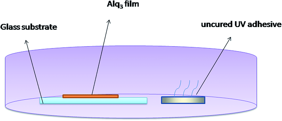 | ||
| Fig. 1 Schematic drawing of Alq3 film treatment process. | ||
The I–V–L characteristics of the OLEDs were measured using a Keithley 2400 source measure unit (Tektronix) and Spectroradiometer SR-UL1R (Topcon). Current efficiency was calculated from the luminance, current density. The angle dependent spectrum was measured by Spectroradiometer SR-UL1R with rotating bracket. The photoluminescence spectrum was measured by FluoroMax-4 (HORIBA), and the transmission and optical haze were measured by UV-2550 with integrating sphere accessory (Shimadzu).
3. Results and discussion
UV adhesive is usually used to seal the cover glass and substrate in OLED encapsulation, the results suggest that the active ingredient of uncured UV adhesive is hazardous to OLED material, so in OLED encapsulation the OLED device should expose to uncured UV adhesive as short as possible. As can be seen from Fig. S1 in the ESI,† depositing 100 nm aluminum on vapor treated Alq3 film, the film exhibits a milky appearance, which suggests that the film become corrugated. The uncured UV adhesive might have a solvent effect on Alq3 molecular, and through the intermolecular force Alq3 molecular move and migrate, at last the film become uneven. Fig. 2 shows the surface morphologies of Alq3 film with different vapor treated time, as can be seen, the untreated Alq3 film (Fig. 2a) shows very smooth surface with roughness 1.8 nm. And with vapor treatment for 1 h (Fig. 2b), the film appears holes and circle patterns with different sizes, the image suggests that uncured UV resin might enter the film through the small holes, and cause dissolution and crystallization of the film. Fig. 2c and d shows the 2 h and 12 h vapor treatment of Alq3 film, after more than two hours of treatment, the film becomes corrugated, and the roughness changes to about 26 nm. The AFM images suggest that under uncured UV adhesive atmosphere, the Alq3 film was dissolved through small holes on the surface and become different sizes of nano grains as shown in Fig. 2c and d.14,15 | ||
| Fig. 2 AFM image of surface morphologies of Alq3 film with different vapor treated times, (a) 0 h, (b) 1 h, (c) 2 h, (d) 12 h. | ||
Fig. 3a shows the photoluminescence (PL) spectrum of vapor treated and untreated Alq3 film, the PL spectrum of vapor treated Alq3 film shows about 20 nm blue shift compared with untreated film. The blue shift of vapor treated Alq3 film might be caused by nano-sized surface roughness which prevents Alq3 molecules from aggregation and thus weakens the interaction between them.11 Fig. 3b shows the transmission of 50 nm vapor treated and untreated Alq3 film, compared with untreated Alq3 film, the transmittance of vapor treated film decrease especially in low wavelength, which is corresponding to the scattering effect of film roughness.
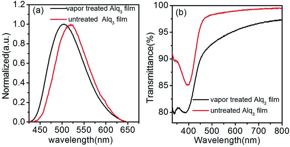 | ||
| Fig. 3 (a) Photoluminescence (PL) spectrum of vapor treated and untreated film. (b) Transmittance spectrum of vapor treated and untreated film. | ||
The scattering of light by surface roughness can be represented by optical haze, which shows the clarity of objects through medium. The optical haze can be used to explain the decrease of the transmittance of vapor treated film, the optical haze can be measured by standard UV/vis spectrophotometer with integrating sphere accessory, the method is shown in Fig. 4a, the haze value can be calculated by following equation:16,17
| Haze = [(T4/T2) − (T3/T1)] × 100% |
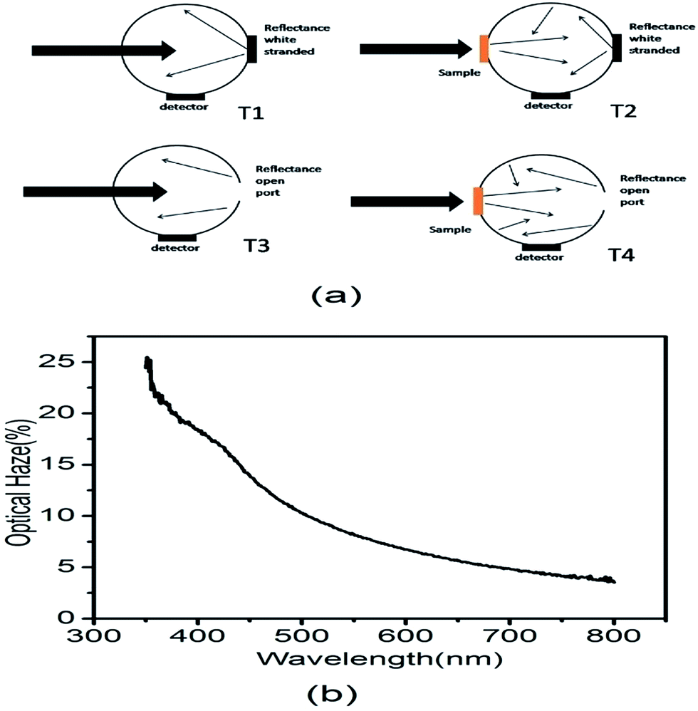 | ||
| Fig. 4 (a) Experimental haze measurement setup (b) optical haze as a function of wavelength of 50 nm vapor treated film. | ||
As we know, the refractive index is approximately 1.7 while the refractive index of glass substrate is 1.4, so when the film become rough, the film would scatter light. The optical haze value of corrugated Alq3 film is shown in Fig. 4b, the optical haze value can be 25% at 350 nm, and decrease to 5% with wavelength increasing, this phenomenon corresponds to the variation of transmittance in Fig. 2b. The optical haze is caused by scattering of light caused by irregularities in the surface, the short wavelength is more easily scattered so the optical haze value decrease with wavelength increasing.
The vapor treated Alq3 film is used in top-emitting organic light-emitting diodes(OLED) device, the device structure is Alq3 (50 nm)/Al (100 nm)/MoO3 (5 nm)/NPB (60 nm)/Alq3 (40 nm)/LiF (1 nm)/Al (10 nm)/NPB (50 nm), the schematic device structure is shown in Fig. 5a, device 1 is deposited on 50 nm vapor treated Alq3 film and device 2 is used as for comparison. The electroluminescence (EL) spectrum is shown in Fig. 5b, as we know, strong microcavity effects exist in top-emitting OLEDs because of semitransparent metal 10 nm aluminum used as top electrode.18 In device 2, the EL spectrum is obviously blue shifted by microcavity effect, however EL spectrum of device 1 is almost the same as PL of Alq3 film, which suggests the microcavity effect is much weakened. As seen in Fig. 5a, device 1 is deposited on corrugated Alq3 film, the light is emitted from NPB/Alq3 interface, and can be scattered in any direction. In microcavity OLEDs, light waves is manipulated by wide-angle and multiple-beam interference, so the radiation characteristic of the device can be changed by optical thickness of the organic layers. When the interface is corrugated, wide-angle and multiple-beam interference no longer exist, so the microcavity effect is greatly reduced in device 1 and the EL spectrum is similar as the PL spectrum of Alq3 film.
 | ||
| Fig. 5 (a) Schematic drawing of device structure of device 1 and device 2 (b) EL spectrum of device 1 and device 2, and PL spectrum of 50 nm Alq3 film. | ||
Fig. 6a shows the I–V–L of two devices, the current density and EL intensity of device 1 is a bit larger than device 2, which is caused by the leakage current induced by corrugated film, the current efficiency in shown in Fig. 6b. At low voltage, the current efficiency of device 1 is significantly less than that of device 2, and with the voltage rise, the current efficiency of the device 1 is gradually larger than the device 2. This phenomenon can be explained by the leakage current of the device, the corrugated film can increase the surface area and may form non emitting regions, which can significantly reduce the current efficiency of device 1, as voltage increase the current increase as the power law of voltage, and the proportion of leakage current decrease, so as voltage increase the current efficiency of device 1 gradually increase.
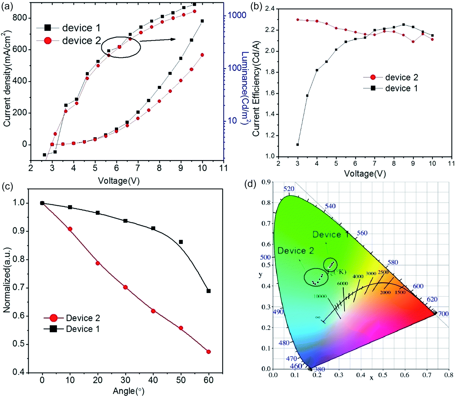 | ||
| Fig. 6 (a) I–V–L of device 1 and device 2. (b) Current efficiency of device 1 and device 2. (c) Normalized EL as a function of angle of device 1 and device 2. (d) Color coordinates of the device 1 and device 2. | ||
The angle dependent of EL is shown in Fig. 6c, compared with the EL of device 1, the EL of device 2 decrease rapidly with angle increasing. In device 1 the EL changes smoothly with angle, the EL intensity only dropped by 10%, and device 2 dropped by 40%, which suggests device 1 has a higher EL efficiency. By integrating the EL of different angles, we get the total EL intensity of device 1 is 28% higher than that of device 2. SPP mode is excited by metal surface, in top-emitting diodes, both electrodes are comprised of metal, so the energy lost in SPP mode is significant. In device 1, because of the corrugated surface, the light trapped in SPP mode can be scattered, we observed an increase of EL efficiency. So we attribute the increase of EL efficiency to scattering of surface plasma mode by corrugated surface. Fig. 6d shows the color coordinates with viewing angle increases from 0° to 60°, due to the scattering effect of corrugated surface, the color coordinates of device 1 shifts smaller than device 2 when viewing angle increases from 0° to 60°.
4. Conclusion
In conclusion, the roughness of 50 nm Alq3 film exposed to uncured UV adhesive whose active ingredient is acrylate monomer is changed from 1.8 nm to 26 nm, which might be caused by forming different sizes of nano grains under uncured UV adhesive atmosphere. The PL and absorption property of vapor treated film is changed by the corrugated surface. The vapor treated film become misty and the optical haze was measured and analyzed. Top-emitting OLED device is deposited on the vapor treated film, the EL spectrum was changed through reduced microcavity by corrugated film, the device efficiency was improved 28% by introducing the corrugated film.Conflicts of interest
There are no conflicts to declare.Acknowledgements
This work was supported by the Fundamental Research Funds for the Central Universities of China (JZ2016HGBZ1027), the Fundamental Research Funds for the Central Universities of China (Grant No. JD2016JGPY0007),the National High Technology Research and Development Program of China (Grant No. 2012AA011901), the National Program on Key Basic Research Project of China (Grant No. 2012CB723406), the National Natural Science Foundation of China (Grant No. 51573036), the Industry-University-Research Cooperation Project of Aviation Industry Corporation of China (Grant No. CXY2013HFGD20).References
- M. K. Fung, Y. Q. Li and L. S. Liao, Adv. Mater., 2016, 28, 10381–13408 CrossRef CAS PubMed.
- T. Chiba, Y. J. Pu and J. Kido, Top. Curr. Chem., 2016, 374, 33 CrossRef PubMed.
- T. Furukawa, H. Nakanotani, M. Inoue and C. Adachi, Sci. Rep., 2015, 5, 8429 CrossRef CAS PubMed.
- H. Sasabe and J. Kido, J. Mater. Chem. C, 2013, 1, 1699–1707 RSC.
- K. Saxena, V. K. Jain and D. S. Mehta, Opt. Mater., 2009, 32, 221–233 CrossRef CAS.
- M. K. Wei, C. W. Lin, C. C. Yang, Y. W. Kiang, J. H. Lee and H. Y. Lin, Int. J. Mol. Sci., 2010, 11, 1527–1545 CrossRef CAS PubMed.
- E. Wrzesniewski, S. H. Eom, W. Cao, W. T. Hammond, S. Lee and E. P. Douglas, et al., Small, 2012, 8, 2647–2651 CrossRef CAS PubMed.
- Y. Qu, C. Coburn, D. Fan and S. R. Forrest, ACS Photonics, 2017, 4, 363–368 CrossRef CAS.
- Y. Chung, H. Yang, X. Xing, M. Zhang, B. Qu and Z. Chen, et al., Sci. Sin.: Chim., 2013, 43, 418–426 CrossRef.
- J. Feng, T. Okamoto, J. Simonen and S. Kawata, Appl. Phys. Lett., 2007, 90, 081106 CrossRef.
- G. S. Huang, X. L. Wu, Y. Xie, F. Kong, Z. Y. Zhang and G. G. Siu, et al., Appl. Phys. Lett., 2005, 87, 151910 CrossRef.
- A. Fujiki, T. Uemura, N. Zettsu, M. Akai-Kasaya, A. Saito and Y. Kuwahara, Appl. Phys. Lett., 2010, 96, 043307 CrossRef.
- J. Feng, Y.-F. Liu, Y.-G. Bi and H.-B. Sun, Laser Photonics Rev., 2017, 11, 1600145 CrossRef.
- J. Gao, L. Duan, G. Yang, Q. Zhang, M. Yang and Q. Fu, Appl. Surf. Sci., 2012, 261, 528–535 CrossRef CAS.
- W. Cai, P. Liu, Y. Jin, Q. Xue, F. Liu and T. P. Russell, et al., Adv. Sci., 2015, 2, 1500095 CrossRef PubMed.
- C. Preston, Z. Fang, J. Murray, H. Zhu, J. Dai and J. N. Munday, et al., J. Mater. Chem. C, 2014, 2, 1248–1254 RSC.
- S. Alomairy, Doctoral dissertation, University of Surrey, 2015.
- W. Wang, H. Peng, S. Wang and S. Chen, Org. Electron., 2015, 24, 195–199 CrossRef CAS.
Footnote |
| † Electronic supplementary information (ESI) available. See DOI: 10.1039/c7ra11384f |
| This journal is © The Royal Society of Chemistry 2017 |