
 Open Access Article
 This Open Access Article is licensed under a
 Creative Commons Attribution 3.0 Unported Licence
Selective metallic coating of 3D-printed microstructures on flexible substrates†
Kuan-Ming Huanga,
Shang-Chen Tsaia,
Yu-Kuan Leeb,
Cheng-Kai Yuanb,
Yu-Ching Changb,
Hsien-Lung Chiua,
Tien-Tung Chung*b and
Ying-Chih Liao *a
*a
aDepartment of Chemical Engineering, National Taiwan University, 114, Taipei, Taiwan. E-mail: liaoy@ntu.edu.tw
bDepartment of Mechanical Engineering, National Taiwan University, 114, Taipei, Taiwan. E-mail: ttchung@ntu.edu.tw
First published on 7th November 2017
Abstract
In this work, a simple method was developed to fabricate micron scale three-dimensional (3D) conductive objects on a flexible PDMS substrate. 3D microstructures were fabricated by the two photon polymerization (TPP) technique and metalized by a subsequent electroless plating step. The PDMS substrate was pre-treated with plasma to develop temporary compatible wettability of the photopolymerizable resin Ormocomp monomer. After the TPP fabrication, hydrophilic 3D microstructures were printed and adhered well to the PDMS surfaces, which recovered hydrophobicity after the TPP process. The printed 3D microstructures were then activated and immersed in an electroless copper plating bath. Due to the hydrophilicity differences, conformal conductive coatings were selectively and uniformly deposited on the 3D microstructures. Several 3D metallic microstructures with complex shapes were demonstrated to show the potential aspects of applying this technology for flexible 3D conductive objects.
Introduction
Recently, research on patterning conductive metallic features on flexible substrates have attracted extensive attention due to the rapid development of wearable electronics and optoelectronic devices.1–3 To achieve fast and accurate patterning, many promising printing techniques have been proposed to replace conventional semiconductor technologies for conductive metallic pattern fabrication.4,5 These printing methods so far not only can produce conductive track patterns on flexible plastic substrates with roll-to-roll mass production, but can also print features accurately with sizes down to the micro-meter scale to meet the demands of applications like micro-electronics and microsensors. On the other hand, challenges remain unresolved to reach a technologically important goal: extending the printed structural dimensionality to the third dimension.6–8 Three-dimensional printed conductive patterns can actually provide a better synthetic route for optoelectronic applications such as metamaterials, which are composed of an array of artificially structured metallic microstructures.9–11 Many striking optical or electromagnetic phenomena, such as negative refraction,12,13 magnetic resonance,14 super lensing,15 and sensing,16 have been demonstrated through the interaction between electromagnetic waves and metamaterials in the literature. Moreover, recent research has shown the feasibility of applying three-dimensional conductive patterns on electronic applications, such as sensors, electrodes, and wireless devices.17–19 However, it is difficult to achieve both miniaturization and true three-dimensional metallic features. Moreover, rendering the substrate flexibility is attracting much research interests. Compared with conventional rigid substrate such as glass or silicon, flexible and stretchable elastomer-based substrates have great advantages of flexibility, conformal manipulation, and lower costs.20–22Most of 3D conductive patterns in the literature are fabricated using a layer-by-layer strategy with planar lithography techniques.23 To produce 3D metallic split ring resonators, Kebin et al. used an approach based on multilayer photoresist coating and electroplating.24,25 Gansel et al. obtained gold helices by exposing helical cavities in a photoresist by direct laser writing, and subsequently filled the cavities with gold by electroplating.10 Although these studies have addressed the issues for 3D metal microstructures, it is still cumbersome and time consuming to produce complex 3D metallic microstructures by using these methods.9
On the other hand, combining microfabrication techniques and electroless plating provides a simple and effective alternative for 3D conductive microstructures. Electroless plating is a popular and mature technique to create metallic coating on plastic objects, including 3D printed plastic parts.26,27 However, although electroless plating is a commonly-used approach to achieve conformal metal coating on plastic surfaces, challenge remains to achieve selective coating on specific locations. Trace metal particle residues can still form on substrate and results in shorted electrical circuits or the low-performance of 3D metal structures.9,28–30 To avoid this problem, commonly, a large UV dose or plasma pretreatment is needed to modify the surface chemical properties to selectively activate the structures.29,31,32 By controlling the energy dose carefully, metal particles can preferentially nucleate on the structure surface. However, these techniques are demonstrated on rigid substrates and restrict their potential applications in flexible electronics.
In this study, we develop a simple method to create 3D conductive structures on a flexible PDMS substrate, which is a commonly used flexible materials for electronic applications.20 To create microstructures with structural resolution down to micron size, two photon polymerization (TPP) technique, an advanced 3D printing technology for microstructures,33–35 is used here. A photosensitive TPP resin, Ormocomp, is selected as the microstructural material due to its good chelating ability to silver ions, which can activate plastic surface for electroless plating and thus metal can be easily plated on Ormocomp to form highly adhesive metal layers. Due to the hydrophobic and chemical inert nature of PDMS, silver ions is incapable to activate PDMS surface and yield in good selectivity in the metallization processes for 3D microstructures. Finally, several microstructures with metal coatings will be demonstrated to show the potential of this technique on the fabrication of 3D conductive structures.
Experimental section
Fabrication of PDMS substrate
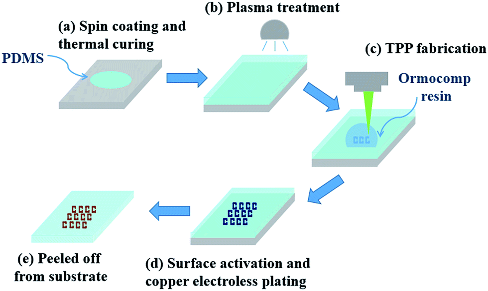
The schematic diagram of the fabrication procedures is shown in Fig. 1. PDMS was prepared by mixing monomer and curing agent (Sylgard 184A, Dow Corning) at a ratio of 10![[thin space (1/6-em)]](https://www.rsc.org/images/entities/char_2009.gif) :1. Appropriate amount of PDMS solution was then poured onto a clean glass slide, which was used as the carrier substrate to support the following TPP processes. PDMS thin film was then prepared by spin coating for 20 s at 2000 rpm, baking for 2 hours at 70 °C. Because of hydrophobic nature of PDMS surface, the sample was processed by air plasma (Eastern Sharp Co., Taiwan) for 60 s to ensure the wettability in the following TPP fabrication processes.
:1. Appropriate amount of PDMS solution was then poured onto a clean glass slide, which was used as the carrier substrate to support the following TPP processes. PDMS thin film was then prepared by spin coating for 20 s at 2000 rpm, baking for 2 hours at 70 °C. Because of hydrophobic nature of PDMS surface, the sample was processed by air plasma (Eastern Sharp Co., Taiwan) for 60 s to ensure the wettability in the following TPP fabrication processes.
 | ||
| Fig. 1 Schematic diagram of the fabrication procedures. Patterns were produced using TPP technique or printed by dispenser following by electroless plating. | ||
Microstructure fabrication
In TPP processes, a drop (∼1 μL) of a commonly used resin Ormocomp (Microresist Co., Germany) was dripped on the aforementioned plasma treated PDMS substrate. 3D microstructures were then fabricated at the focusing point of an Nd-Yag laser (532 nm, 130 kHz, 26 mW). After the TPP fabrication, the sample is washed by methyl isobutyl ketone (MIBK) and acetone to remove the remaining uncured Ormocomp resin.Surface-metallization of microstructure
Before electroless plating, the samples are immersed in 10 wt% silver nitrite solution for 90 s to activate the Ormocomp surfaces. Copious rinsing was carried out after the activation step to avoid absorption of unattached silver ions on PDMS. The electroless bath formulation was from our previous study.36 The plating solution consisted of 2.7 g of CuSO4·5H2O (Sigma Aldrich), 8.15 g of sodium potassium tartrate (J. T. Baker), 3.25 g of NaOH (Mallinckrodt Chemicals), 0.1 L of DI water, and 25 mL of an aqueous solution of glyoxal (40 wt%, Alfa Aesar). The activated 3D-printed samples were then immersed in electroless plating solution at 55 °C for 70 s and then rinsed with DI water. The samples were dried at room temperature under atmospheric pressure. Finally, PDMS is peeled off from the glass slide carefully. For electroless silver plating, the plating solution consists of silver ammonia solution and 10 wt% glucose solution at a weight ratio of 1:12. The silver ammonium solution, or the so-called Tollens' reagent, was prepared by the following steps. 12.5 wt% AgNO3 aqueous solution and 4 wt% NaOH aqueous solution were mixed at a weight ratio of 1:1.25. Concentrated ammonia was then added dropwise until all the Ag2O solid precipitate dissolved totally. The plating process was conducted at a temperature of 35 °C for 1 minute.
Contact angles of Ormocomp solution on PDMS were measured by dripping 1 μL of liquid drops on the surface. The contact angle was observed by an in-house goniometer. The composition and morphology of copper thin film were determined by scanning electron microscopy (Nova NanoSEM 230) with an accelerating voltage of 5 kV. The crystalline structure was examined with X-ray diffractometer (Rigaku Ultima IV) using a 2θ angle ranging from 15 to 80 degree with a 0.02-degree step size.
Results and discussion
The adhesion of Ormocomp resin on PDMS is crucial to the microstructure fabrication. After TPP process, the printed microstructures on pristine PDMS disappeared after removing the excessive uncured Ormocomp liquid with solvent rinse, possibly due to the weak adhesion of Ormocomp micro-structures on hydrophobic PDMS surfaces (Fig. S1†).20 To enhance the adhesion, plasma treatment is used and shows effective improvements on the adhesion (Fig. S1†). To verify the adhesion differences, as shown in Fig. 2(a), millimeter-size straight line patterns are printed with a micro-dispenser and cured on pristine PDMS. The cured patterns detach easily by simply bending the PDMS substrate, showing low affinity between Ormocomp resin and PDMS. | ||
| Fig. 2 Cured Ormocomp threads printed on (a) pristine and (b) plasma-treated PDMS. (c) Time evolution of Ormocomp monomer liquid on PDMS after plasma treatment. The inset pictures show the contact angle of Ormocomp monomer liquid on PDMS. | ||
Plasma treatment on PDMS surface can effectively avoid the delamination or detachment of printed structures (Fig. 2(b)). Ormocomp is a UV-sensitive organic–inorganic hybrid polymer and belongs to the class of Ormocers. The chemical characters of these hybrid organic–inorganic polymers has been known to be compatible with glass because the hydroxyl and alkoxyl groups of Ormocomp can react with the Si–OH groups of the glass surface.37 In literature, PDMS surface can be oxidized by plasma treatment to form Si–OH bonds to improve the surface hydrophilicity.38–40 As shown in Fig. 2(c), after plasma treatment, the contact angle of Ormocomp monomer liquid on PDMS decreases greatly from 61 degree to 15 degree due to strong surface oxidation.38 However, the polymeric structural changes are temporary. The contact angle raises quickly to 32 degree in an hour, indicating the plasma treatment is effective only for a short duration, and gradually increases to 45 degrees after three days. The increase of Ormocomp wettability on PDMS indicates the formation of high energy groups such as Si–OH bond on the surface. These functional groups can react with Ormocomp monomers37 and the chemical bonds enhance the adhesion between PDMS and cured Ormocomp. As shown in Fig. 2(b), the adhesion of Ormocomp on PDMS improves significantly and the printed Ormocomp patterns could withstand a high degree of bending without separation or delamination. Moreover, the printed Ormocomp strips can attach on PDMS substrate with strong adhesion for a long time: the same bending experiment is carried out one month after fabrication, and Ormocomp strips still adhere well on PDMS as those in Fig. 2(b). To create attached 3D structures on PDMS, the samples in the following sections are prepared on PDMS immediately after plasma treatment to ensure surface the wettability.
Electroless plating
To produce uniform metal coatings on Ormocomp structures, a simple electroless plating method is applied here. Silver nitrate is used here to serve as a seeding catalyst for electroless metal deposition and help the creation of plated copper thin film on polymer surfaces.36 As shown in Fig. 3(a), 1 μL Ormocomp monomer liquid is dropped on PDMS by a dispenser and then cured by UV light to form a circular lens with approximately 300 μm in radius (Fig. 3(b)). After submerged in silver nitrate solution, a catalytic layer selectively coated over the circular lens can be observed clearly from the EDX image (Fig. 3(c)). A clear contrast between the Ormocomp lens (green regions) and PDMS (black regions) confirms that silver catalysts are deposited. The catalyst selectivity can be attributed to the hydrophilicity differences between PDMS and Ormocomp surfaces. Although after the plasma treatment, both PDMS and Ormocomp become hydrophilic, the PDMS surface recovers the hydrophobicity in a few minutes (Fig. S2†) while the Ormocomp remains hydrophilic.30,38,41 Due to the hydrophobicity, the seeding agent (aqueous silver nitrate solution) cannot activate the PDMS surface and leaves PDMS surfaces uncoated in the electroless plating process. On the other hand, Ag+ ions can absorbed onto Ormocomp surfaces, possibly due to the existence of electron donating ligands in Ormocomp molecular structure such as thioether and alkoxyl groups,42 which can attract silver ions through electrostatic interactions.43 The absorbed silver ions on Ormocomp serve as seeds for autocatalytic copper recovery in electroless plating bath. After the plating process, the lenses are coated with a copper layer and show shiny luster under room lights (Fig. 3(d)). The lens structure after the plating bath remain intact on the PDMS (Fig. 3(e)), indicating the adhesion between Ormocomp and PDMS is strong enough to survive in the basic plating bath. Moreover, the EDX results show that copper layers only grow on Ormocomp and leave PDMS surface uncoated (Fig. 3(f)). The metallized lens area has a strong adhesion on PDMS. As shown in Fig. S3,† the circular lens array on PDMS adheres fairly well with good mechanical stability even under stretching conditions. To examine the adhesion of the plated copper layers, Ormocomp thin film are coated on PDMS by bar coating. After the subsequent seeding and electroless plating steps, a continuous copper layer (Fig. S4†) with a shiny red color can be obtained. The plated copper thin films attach well to the substrate and remain complete under tape tests (Fig. S4†). The conductivity of the plated copper thin films depends strongly on the plating time. To optimize the plating time, Ormocomp threads of 500 μm in width (Fig. 4(b)) and 2 cm in length are immersed in copper plating bath for various times. As shown in Fig. 4(a), for deposition time longer than 70 s, the resistance remains constant and plateaus. The SEM image (Fig. 4(c)) shows that the copper thin films are composed of closely packed spherical grains of 20 to 30 nm in diameter. Moreover, from the cross-sectional SEM image, the continuous copper thin film has a thickness of 150 nm (Fig. 4(d)) after electroless deposition for 70 s. The resistivity of the plated copper thin film is about 2.8 × 10⁻⁸ Ω m, about 1.75 times of the resistivity of bulk copper. | ||
| Fig. 3 (a) Picture of cured Ormocomp circular lenses. (b) SEM image of a circular lens on sample (a) after processed with silver nitrate activation step. (c) The EDX image of (b) showing silver distribution. (d) Picture of cured Ormocomp circular lenses coated with copper thin films. (e) SEM image of a circular lens in (d). (f) EDX image of (e) showing copper distribution. | ||
 | ||
| Fig. 4 (a) Resistance of plated copper thin films on Ormocomp threads versus the immersion time in copper plating bath. (b) Picture of copper plated Ormocomp threads. (c) Top view SEM image of deposited copper thin films after 70 s deposition. (d) The cross-sectional view of (c). | ||
Basic elemental analysis
To identify the chemical composition of the plated copper thin film on Ormocomp, energy-dispersive X-ray (EDX) spectrum is used to examine the sample (Fig. 5(a)). The results confirm the existence of copper with other chemical elements such as C, O, Si, and S, which can be found in the molecular structure of Ormocomp. Trace silver signals are also found in EDX results, due to the silver nitrate catalyst used in the activation step before electroless copper plating. X-ray diffraction (XRD) patterns is also used to further examine the crystalline structures of plated copper layers (Fig. 5(b)). A characteristic reflection peak at 44° indicates the (111) plane Bragg's reflections of face-centered-cubic (FCC) copper structure. No obvious copper oxide peaks are found, indicating little oxidation occurs after the copper thin film synthesis. | ||
| Fig. 5 (a) EDX spectrum and (b) XRD patterns for plated copper thin films. | ||
Metallized 3D microstructures
3D microstructures with copper coatings can be fabricated by TPP and subsequent electroless plating steps. Fig. 6(a) shows the SEM image of a 3D printed micro coil with copper plating. With the ability of TPP, one can create 3D micro structures easily. The subsequent activation step only activates the Ormocomp surfaces, as shown previously in Fig. 3. Thus, selective metal coatings with good coverage are found only on the 3D Ormocomp structures (Fig. 6(b)). The inset picture in Fig. 6(a) shows the surface morphology of the copper coating on the printed 3D structures on a PDMS substrate. The image reveals that thick and continuous copper coatings are deposited uniformly on Ormocomp surfaces. Fig. 6(b) shows the EDX mapping image and reveals that metal deposition mainly occurred on Ormocomp without contaminating PDMS substrate, indicating great selectivity of the metallization process on 3D microstructures. We also fabricated 3D split ring resonators covered with copper by using the aforementioned TPP/electroless plating method, as shown in Fig. 6(c). These ring resonators comprise of beams of 5 μm width. After electroless plating steps, the plated copper thin films only grow on 3D structures and show a shiny copper luster, as indicated in the top-side view optical microscopy image in Fig. 6(d). Besides, the sample can attach on curve surface in a conformal manner (Fig. 6(d)). The structures adhere well to PDMS even after repeated bending, illustrating the potential of this technique on fabricating flexible metamaterials. Using the same technique, one can also fabricate microstructure with silver coatings by electroless silver plating (Fig. 7(a)). Similarly, only Ormocomp surfaces are activated and thus silver layers grow on selectively on the printed structures (Fig. 7(c)) rather than the PDMS surfaces (Fig. 7(b)). The EDX analysis also confirms that the nanoparticles deposited on the structure are silver (Fig. 7(d)). These examples demonstrate the feasibility of applying this method in fabricating conductive parts for flexible electronics.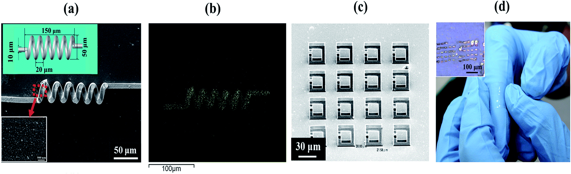 | ||
| Fig. 6 (a) CAD design and SEM images of a 3D micro coil. The Ormocomp is coated with copper thin film using electroless plating as shown in the inset SEM images. (b) EDX mapping image of sample (a). The yellow color shows copper distribution. (c) SEM image of a 3D split ring resonator array. (d) A picture of sample (c) to demonstrate the flexibility. | ||
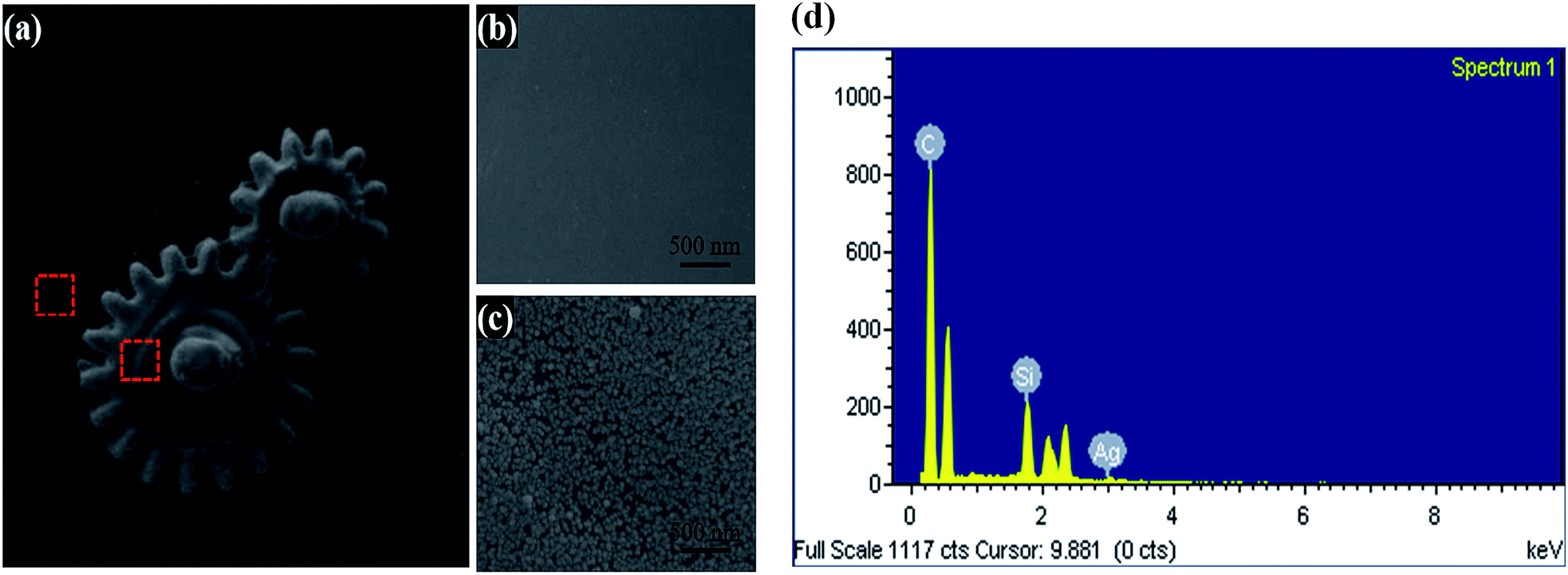 | ||
| Fig. 7 (a) SEM image of a 3D printed micro-gear. The Ormocomp surface is coated with silver layer using electroless silver plating. (b) Surface morphology on the PDMS substrate and (c) the gear structure. (d) EDX spectrum of the plated layer on the gear surface. | ||
Conclusions
In this study, a simple method is developed to fabricate 3D microstructures with conductive metal coatings on PDMS substrate. The structures are fabricated by two photon polymerization technique and metallized by subsequent electroless plating steps. A plasma treatment was used to develop compatible wettability between the photopolymerizable resin Ormocomp monomer and PDMS substrate. The samples were then immersed in copper plating bath for 70 s at 55 °C and copper thin films were successfully deposited on the 3D structures with conformal coating. Due to the chemical nature differences, the metal layers grow preferentially on the 3D-printed Ormocomp structures rather than the PDMS substrates. Several exemplar 3D objects with complex geometries are also demonstrated to show the coating uniformity and substrate selectivity. This study provides a general guideline for 3D conductive pattern formation and demonstrate the feasibility to fabricate micron-size features with arbitrary geometries on flexible substrates. This method can be further extended to other 3D printing systems and opens a new avenue to potential applications in flexible electronics.Conflicts of interest
There are no conflicts to declare.Acknowledgements
The authors are grateful to the Ministry of Science and Technology (MOST) of Taiwan for supporting this study.Notes and references
- M. Stoppa and A. Chiolerio, Sensors, 2014, 14, 11957–11992 CrossRef CAS PubMed.
- T. Inui, H. Koga, M. Nogi, N. Komoda and K. Suganuma, Adv. Mater., 2015, 27, 1112–1116 CrossRef CAS PubMed.
- N. Yu and F. Capasso, Nat. Mater., 2014, 13, 139–150 CrossRef CAS PubMed.
- B. W. An, K. Kim, M. Kim, S. Y. Kim, S. H. Hur and J. U. Park, Small, 2015, 11, 2263–2268 CrossRef CAS PubMed.
- W. Shen, X. Zhang, Q. Huang, Q. Xu and W. Song, Nanoscale, 2014, 6, 1622–1628 RSC.
- C. Ladd, J. H. So, J. Muth and M. D. Dickey, Adv. Mater., 2013, 25, 5081–5085 CrossRef CAS PubMed.
- B. Y. Ahn, E. B. Duoss, M. J. Motala, X. Guo, S.-I. Park, Y. Xiong, J. Yoon, R. G. Nuzzo, J. A. Rogers and J. A. Lewis, Science, 2009, 323, 1590–1593 CrossRef CAS PubMed.
- T. Tanaka, A. Ishikawa and S. Kawata, Appl. Phys. Lett., 2006, 88, 081107 CrossRef.
- A. Radke, T. Gissibl, T. Klotzbücher, P. V. Braun and H. Giessen, Adv. Mater., 2011, 23, 3018–3021 CrossRef CAS PubMed.
- J. K. Gansel, M. Thiel, M. S. Rill, M. Decker, K. Bade, V. Saile, G. von Freymann, S. Linden and M. Wegener, Science, 2009, 325, 1513–1515 CrossRef CAS PubMed.
- I. Staude, M. Decker, M. J. Ventura, C. Jagadish, D. N. Neshev, M. Gu and Y. S. Kivshar, Adv. Mater., 2013, 25, 1260–1264 CrossRef CAS PubMed.
- A. Boltasseva and V. M. Shalaev, Metamaterials, 2008, 2, 1–17 CrossRef.
- D. R. Smith, J. B. Pendry and M. C. Wiltshire, Science, 2004, 305, 788–792 CrossRef CAS PubMed.
- A. Sihvola, Metamaterials, 2007, 1, 2–11 CrossRef.
- D. Schurig, J. Mock, B. Justice, S. A. Cummer, J. B. Pendry, A. Starr and D. Smith, Science, 2006, 314, 977–980 CrossRef CAS PubMed.
- T. Chen, S. Li and H. Sun, Sensors, 2012, 12, 2742–2765 CrossRef PubMed.
- J. T. Muth, D. M. Vogt, R. L. Truby, Y. Mengüç, D. B. Kolesky, R. J. Wood and J. A. Lewis, Adv. Mater., 2014, 26, 6307–6312 CrossRef CAS PubMed.
- B. W. An, K. Kim, H. Lee, S. Y. Kim, Y. Shim, D. Y. Lee, J. Y. Song and J. U. Park, Adv. Mater., 2015, 27, 4322–4328 CrossRef CAS PubMed.
- Y. Jo, J. Y. Kim, S.-Y. Kim, Y.-H. Seo, K.-S. Jang, S. Y. Lee, S. Jung, B.-H. Ryu, H.-S. Kim and J.-U. Park, Nanoscale, 2017, 9, 5072–5084 RSC.
- S. Walia, C. M. Shah, P. Gutruf, H. Nili, D. R. Chowdhury, W. Withayachumnankul, M. Bhaskaran and S. Sriram, Appl. Phys. Rev., 2015, 2, 011303 Search PubMed.
- J. Joshi, S. S. Pattnaik and S. Devi, Int. J. Antenn. Propag., 2012, 2012, 974315 Search PubMed.
- X. Xu, B. Peng, D. Li, J. Zhang, L. M. Wong, Q. Zhang, S. Wang and Q. Xiong, Nano Lett., 2011, 11, 3232–3238 CrossRef CAS PubMed.
- Y. Xie, S. Ye, C. Reyes, P. Sithikong, B.-I. Popa, B. J. Wiley and S. A. Cummer, Appl. Phys. Lett., 2017, 110, 181903 CrossRef.
- F. Kebin, C. S. Andrew, D. A. Richard and Z. Xin, J. Micromech. Microeng., 2012, 22, 045011 CrossRef.
- K. Fan, A. Strikwerda, H. Tao, X. Zhang and R. Averitt, 3D stand-up metamaterials with a purely magnetic resonance at terahertz frequencies, OSA/CLEO/QEL conference on Laser Science to Photonic Applications, IEEE Xplore, 2010, DOI:10.1109/MEMSYS.2010.5442338.
- R. L. Macary and R. Hamilton, Met. Finish., 2010, 108, 35–37 CrossRef CAS.
- J. R. Jian, T. Kim, J. S. Park, J. Wang and W. S. Kim, AIP Adv., 2017, 7, 035314 CrossRef.
- M. M. Hossain and M. Gu, Laser Photonics Rev., 2014, 8, 233–249 CrossRef CAS.
- Y. Yan, M. I. Rashad, E. J. Teo, H. Tanoto, J. Teng and A. A. Bettiol, Opt. Mater. Express, 2011, 1, 1548–1554 CrossRef CAS.
- F. Formanek, N. Takeyasu, T. Tanaka, K. Chiyoda, A. Ishikawa and S. Kawata, Appl. Phys. Lett., 2006, 88, 083110 CrossRef.
- W. Dai and W. Wang, Sens. Actuators, A, 2007, 135, 300–307 CrossRef CAS.
- A. A. Bettiol, Y. Yan, E. J. Teo, H. Tanoto and J. Teng, Radio frequency plasma pre-treatment for selective electroless Ag coating of three-dimensional SU-8 microstructures, Proceedings of the SPIE, 2012, vol. 8249, p. 824916 Search PubMed.
- J.-F. Xing, M.-L. Zheng and X.-M. Duan, Chem. Soc. Rev., 2015, 44, 5031–5039 RSC.
- A. Ostendorf and B. N. Chichkov, Photonics Spectra, 2006, 40, 72 Search PubMed.
- H.-B. Sun and S. Kawata, in NMR 3D Analysis Photopolymerization, Springer, 2004, pp. 169–273 Search PubMed.
- Y.-C. Liao and Z.-K. Kao, ACS Appl. Mater. Interfaces, 2012, 4, 5109–5113 CAS.
- J. Kron, S. Amberg-Schwab and G. Schottner, J. Sol-Gel Sci. Technol., 1994, 2, 189–192 CrossRef CAS.
- C.-Y. Li and Y.-C. Liao, ACS Appl. Mater. Interfaces, 2016, 8, 11868–11874 CAS.
- S. Bhattacharya, A. Datta, J. M. Berg and S. Gangopadhyay, J. Microelectromech. Syst., 2005, 14, 590–597 CrossRef CAS.
- C. de Menezes Atayde, Phys. Status Solidi C, 2010, 7, 189–192 CrossRef.
- F. Formanek, N. Takeyasu, T. Tanaka, K. Chiyoda, A. Ishikawa and S. Kawata, Opt. Express, 2006, 14, 800–809 CrossRef CAS PubMed.
- S. Obi, Replicated optical microstructures in hybrid polymers, PhD thesis, Université de Neuchâtel, 2006.
- H. Huang, Q. Yuan and X. Yang, Colloids Surf., B, 2004, 39, 31–37 CrossRef CAS PubMed.
Footnote |
| † Electronic supplementary information (ESI) available. See DOI: 10.1039/c7ra11171a |
| This journal is © The Royal Society of Chemistry 2017 |