
 Open Access Article
 This Open Access Article is licensed under a Creative Commons Attribution-Non Commercial 3.0 Unported Licence
Induction of diffusion and construction of metallurgical interfaces directly between immiscible Mo and Ag by irradiation-induced point defects
Lanting Li,
Jie Zhang,
Xinchang Pan ,
Yuan Huang*,
Zumin Wang and
Yongchang Liu
,
Yuan Huang*,
Zumin Wang and
Yongchang Liu
Institute of Advanced Metallic Materials, School of Material Science and Engineering, Tianjin University, Tianjin 300350, PR China. E-mail: tju_huangyuan@163.com; Tel: +86 13920838071
First published on 22nd November 2017
Abstract
As advanced materials, Mo/Ag laminated metal composites (LMCs) can be used for the interconnectors of spacecraft solar arrays and extend spacecraft orbital lifetime effectively. However, since diffusion alloying is very difficult in immiscible Mo–Ag systems, the preparation of Mo/Ag LMCs with metallurgical bonding interfaces is very difficult. To solve the problem, irradiation-induced point defects (IIPDs) are used to induce diffusion and realize alloying in an immiscible Mo–Ag system in this research. The induction process includes: first, causing IIPDs on the surface of a Mo sheet through ion implantation; secondly, evaporating an Ag layer onto the ion implantation damaged Mo sheet to obtain a Mo/Ag laminated sample; and lastly, annealing treatment for the sample. The measurements adopted in this paper primarily include high-resolution transmission electron microscopy (HRTEM) and variable energy positron annihilation spectroscopy (VEPAS). The microstructure analysis for the Mo/Ag interface proves that the Ag elements diffuse into Mo during the final annealing. The micro-test results also reveal that, along with the diffusion of Ag elements, the IIPDs migrate in the opposite direction from Mo to Ag with a migration distance of ∼77 nm, which agrees well with the diffusion distance of Ag elements (∼79 nm). The calculation results of the diffusion energy barrier (Ea) show that the migrating IIPDs are vacancies. So it can be concluded that IIPDs, especially vacancies, can indeed induce diffusion in an immiscible system, and the diffusion mechanism is most likely the vacancy-assisted mechanism. The Kirkendall voids found in the samples verify the judgment on the diffusion mechanism. Through the induction of diffusion, a metallurgical interface is successfully constructed between immiscible Mo and Ag without using any metal interlayer, indicating that the Mo/Ag LMCs can be prepared by this novel method.
1. Introduction
Mo/Ag laminated metal composites (LMCs) can be used for the interconnectors of spacecraft solar arrays and extend spacecraft orbital lifetime effectively. For example, Mo/Ag LMCs have been used in the Hubble Space Telescope by the European Space Agency (ESA).1 However, since diffusion is difficult in Mo–Ag binary systems, the preparation of Mo/Ag LMCs with metallurgical bonding interfaces is very difficult.Diffusion is one of the fundamental processes, which governs the microstructure, processing, and properties of materials.2 At present, the majority of the studies concerning diffusion have focused on solid-solution systems. The corresponding diffusion mechanisms, mainly including the interstitial diffusion mechanism,3–5 the exchange diffusion mechanism,6,7 and the vacancy-assisted mechanism,8,9 have been suggested. The vacancy-assisted mechanism has been found to be the dominant diffusion mechanism. Under the vacancy-assisted mechanism, a net flow of diffusing atoms in one direction is associated with a net flow of vacancies in the opposite direction.2
However, there are some binary systems, such as Mo–Ag, Mo–Cu, W–Cu, W–Ag and Cu–Ta systems, in which the two constituent elements show little or no mutual solubility at ambient temperature and pressure. These binary systems are usually characterized with a large positive heat of mixing (ΔHm), which are called immiscible metal (or alloy) systems.10 Due to the absence of thermodynamic driving forces and large lattice mismatches,11 diffusion rarely occurs and metallurgical bonding interfaces cannot be constructed directly between the immiscible metals. Therefore, most of the material preparations, e.g., metallic cementation and bonding/composite of metals, are based on solid-solution systems, while immiscible metal systems are rarely considered. When two immiscible metals, for example, W and Cu metals,12,13 need to be connected or combined, a metal interlayer is usually introduced to obtain a metallurgical interface between the two immiscible metals. At present, the Mo/Ag LMCs used in the spacecrafts of the Europe Space Agency (ESA) are still prepared by using a platinum metal interlayer.1
To induce the direct diffusion in an immiscible system, one would have to create artificially thermodynamic driving forces and diffusion paths for the immiscible elements. Aiming at this situation, irradiation-induced point defects (IIPDs) caused by ion implantation is used to induce the diffusion in the Mo–Ag immiscible system in this paper. The reason for the idea, on the one hand, is that, no-equilibrium energy of irradiation-induced defects, e.g., storage energy, can serve as a thermodynamic driving force for the diffusion. On the other hand, IIPDs can provide paths for the diffusion.
To verify the feasibility of the induction of the diffusion in the immiscible Mo–Ag system by IIPDs, laminated samples based on the immiscible Mo–Ag system were prepared and studied in this paper. The process for the preparation of the Mo/Ag laminated sample primarily includes three steps: causing IIPDs in Mo by ion-implantation, evaporation plating an Ag layer on the damaged Mo, and annealing at high temperature, which is also the induction process of the diffusion.
To determine whether the diffusion occurs and identify the interfacial microstructure, scanning electron microscope (SEM), energy dispersive spectrometer (EDS) line scanning and high resolution transmission electron microscope (HRTEM) were used to characterize the cross-section of the Mo/Ag laminated samples. Auger electron spectroscopy (AES) depth profiling was employed to determine the diffusion source of Ag elements. Variable energy positron annihilation spectroscopy (VEPAS), HRTEM and energy dispersive X-ray spectroscopy (EDX) were used to investigate the migration (including migration direction and distance) and evolution of the IIPDs. All of the above analysis results were eventually used to determine whether IIPDs could induce the diffusion, whether a metallurgical interface could form between Mo and Ag, and what the diffusion mechanism was.
According to the results obtained in this paper, it can be proved that IIPDs especially vacancies can indeed induce diffusion in an immiscible system, and the corresponding diffusion mechanism is still the conventional vacancy-assisted mechanism8,9 presented in solid-solution systems. Through the diffusion, a metallurgical interface can be constructed directly between immiscible Mo and Ag. Obviously, the Mo/Ag LMCs can be prepared using this novel method.
2. Materials and methods
2.1. Sample preparation
The preparation process of the Mo/Ag laminated sample is shown in Fig. 1.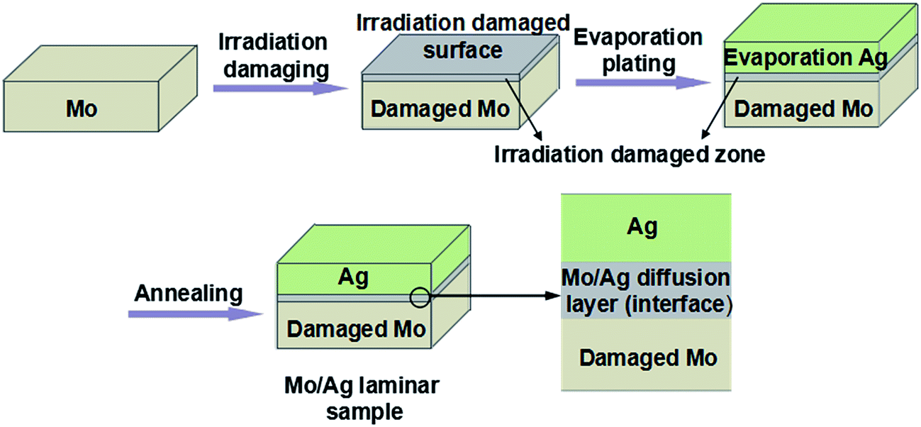 | ||
| Fig. 1 Preparation process of the Mo/Ag laminated sample. | ||
Pure Mo sheets (16 × 16 × 1 mm3) were polished with an abrasive paper (2000-grade) to a mirror flat surface and rinsed with deionized water. After that, the Mo sheets were annealed at 900 °C (ref. 14) in a H2 atmosphere for 8 h to eliminate the defects in Mo.
The pre-annealed pure Mo sheets were irradiated at room temperature in a high current ion implanter (MEVVAII ion source) using Ag+ ions with two decreasing energies (126–42 keV) in turn. During the implantation, the doses were all 3.4 × 10¹⁷ ions cm−2, and the beam intensity was between 2.0 and 2.5 mA.
Then, Ag layers with two thicknesses (100 nm and 5.5 μm) were evaporated onto the ion implantation damaged Mo sheets using vacuum evaporation plating technology. The evaporation sources were pure silver (purity is 99.9999%), and the deposition rates were approximately 1.5 nm s−1.
Finally, the plated specimens were annealed at different temperatures for different times in a H2 atmosphere in a tube furnace. When the annealing was completed, the final Mo/Ag laminated samples were obtained.
2.2. Measurements
In this study, the cross-sectional microstructure of the Mo/Ag laminated sample with a 5.5 μm thick Ag layer annealed at 800 °C for 4 h was characterized by a HITACHI S4800 field-emission SEM equipped with an EDS detector. The microstructure of the as-constructed Mo/Ag interface was also investigated with a Tecanai G2 F20 S-Twin TEM equipped with an EDX analyzer.To determine the diffusion source of Ag elements and investigate the role of ion implantation played in the diffusion, an in-depth distribution of composition in the irradiation damaged Mo samples was analyzed before and after annealing by using AES depth profiling. During the tests, the Ar+ sputtering rates were 56.4 nm min−1 (for SiO2).
VEPAS was employed to analyze the migration and evolution of the IIPDs in the Mo/Ag laminated samples with an Ag layer of 100 nm thickness annealed at a series of temperatures, including 300 °C, 400 °C, 500 °C, 600 °C, 700 °C, 800 °C and 900 °C, for 1.5 h. During the VEPAS tests, the positron beams were injected into the laminated samples from the Ag layer. The pre-annealed pure Mo and irradiation damaged Mo samples were also tested by VEPAS for comparison.
3. Results and discussion
3.1. Occurrence of diffusion and construction of metallurgical interface
SEM morphology of the cross-section of the Mo/Ag laminated sample with a 5.5 μm thick Ag layer annealed at 800 °C for 4 h is shown in Fig. 2a. It can be seen that there are three regions in the cross-section: the Mo layer, the swelling intermediate layer and the vapor-deposited Ag layer. | ||
| Fig. 2 (a) SEM image and EDS line-scanning profile of the cross-section of the Mo/Ag laminated sample. (b) HRTEM image of the Mo/Ag diffusion layer obtained from the area marked by circle A in (a).15 | ||
Fig. 2a also shows that the morphology of the intermediate layer is similar to that of the Mo and there is a middle line separating the layer into two sub-layers.16 The EDS line-scanning profile in Fig. 2a reveals that a concentration gradient distribution of Mo and Ag has been formed in the left sub-layer of the intermediate layer, and the composition is almost entirely Ag in the right sub-layer. Considering the swelling intermediate layer still shows the morphology of the Mo layer, it can be concluded that the Ag elements successfully diffuse into Mo, and the intermediate layer is a Mo/Ag diffusion layer.
Fig. 2b shows a HRTEM image of the Mo/Ag diffusion layer obtained from the area marked by circle A as shown in Fig. 2a, where the inset is the electron diffraction pattern for the diffusion layer. Fig. 2b clearly shows that the Mo/Ag diffusion layer consists of both Ag crystalline phases and Mo/Ag amorphous phases, indicating that the solid state amorphization reaction (SSAR)17 occurs. Obviously, a Mo/Ag metallurgical interface is successfully constructed through the diffusion of the Ag elements.
3.2. Diffusion source of the Ag elements
Where the Ag elements diffuse from is a question that needs to be answered. Fig. 3a shows the in-depth composition profiles in the Ag+-implanted Mo sheet without a vapor-deposited Ag layer before annealing. It can be seen from Fig. 3a that the maximum Ag concentration appears at the near surface region, and there are almost no Ag elements in the deeper region. | ||
| Fig. 3 In-depth composition profiles of the implanted Mo sheets before (a) and after (b) annealing at 800 °C for 4 h.15 | ||
Fig. 3b exhibits the in-depth composition profile in the implanted Mo sheet annealed at 800 °C for 4 h in a H2 atmosphere, from which it can be seen that the Ag content is very low and nearly equal to 0%. These results indicate that the Ag+ ions implanted into the Mo disappear and cannot diffuse to form a concentration gradient distribution during the annealing process.
Comparing the EDS line scanning results shown in Fig. 2a with the AES results shown in Fig. 3b, it can be concluded that it is the Ag elements from the evaporated Ag layer rather than the implanted Ag+ ions that diffuse into Mo when the Mo/Ag laminated sample is annealed. The primary role of the ion-implantation is to cause IIPDs in Mo and induce the inward diffusion of the Ag elements of the outer layer.
3.3. Migration and evolution of irradiation-induced point defects
To determine the mechanism of the diffusion observed in Section 3.1, first of all, the migration and evolution of IIPDs during the diffusion process should be investigated. VEPAS has proven to be a suitable tool for investigations of open-volume and defects in materials.18–21 The most important parameter of VEPAS is the line shape parameter, S. A larger S corresponds to a larger open-volume or a higher defect-concentration.22 Investigations regarding the evolution of IIPDs during the diffusion process were performed using VEPAS in this paper.The VEPAS results are shown in Fig. 4, where Fig. 4a shows the S parameters as a function of positron implantation energy (the positron implantation energy and depth corresponding to the depth of the samples) for the samples including the pre-annealed pure Mo and the Ag+ ion implantation damaged Mo. The S parameters are normalized to the defect-free S value, namely SB,23 of the pre-annealed pure Mo. In Fig. 4a, the SB is roughly equal to 0.430, and the vertical coordinates on the right are given as S/SB.
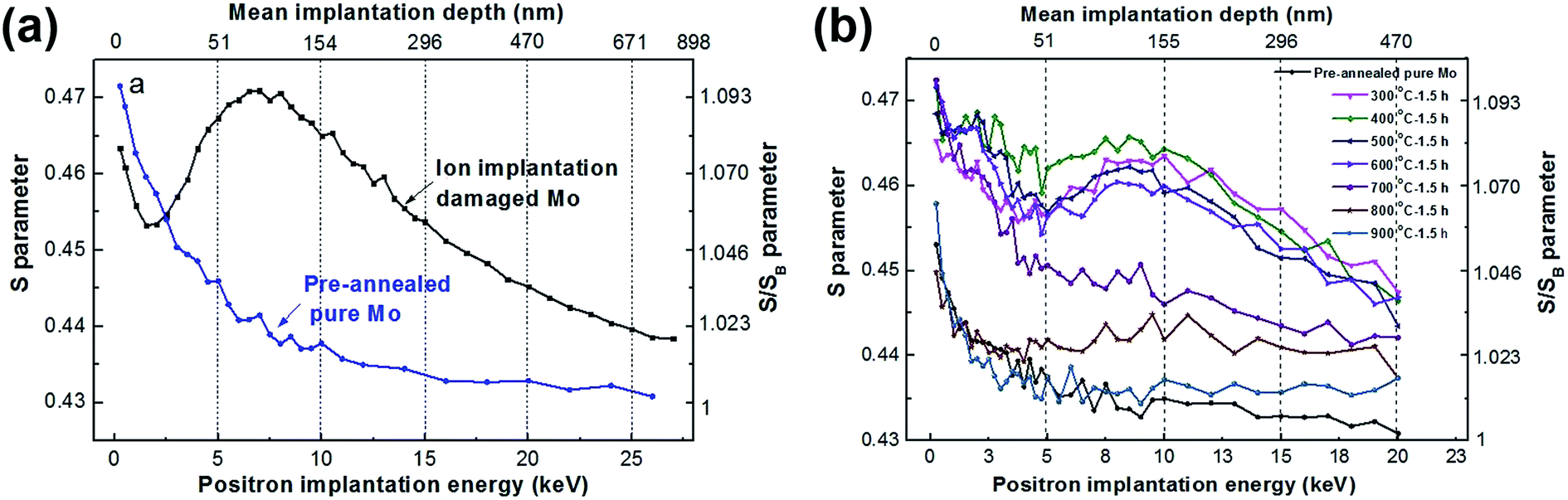 | ||
| Fig. 4 VEPAS results of various samples: (a) S parameter vs. positron implantation energy for the pre-annealed pure Mo and the Ag+ ion-implanted Mo, (b) S parameter vs. positron implantation energy for the pre-annealed pure Mo and the Mo/Ag laminated samples with a 100 nm thick Ag layer annealed at different temperatures. | ||
From Fig. 4a, the high S values can be observed for all of the curves at the near-surface region of the samples, which are due to the surface-related phenomena such as oxide layers and surface contamination.23 With the increase in the depth of the samples, the S parameter of pre-annealed pure Mo decreases and approaches the value ascribed to the defect-free crystalline molybdenum. Conversely, high S-values can be observed in the S curve of the ion-implantation damaged Mo, which intuitively corresponds to the positrons trapped at defects in the damaged region24,25 and reveals that a lot of damages are caused in the Mo by the Ag+ ion irradiation.
Fig. 4b shows the S-parameter curves of the Mo/Ag laminated samples with a 100 nm vapor-plated Ag layer annealed at different temperatures. It can be seen that the peaks of these curves present obvious changes for the samples annealed at different temperatures from 300 °C to 700 °C. The S-parameter values and the corresponding depths of the S peaks18 at different annealing temperatures are shown in Table 1.
| Annealing temperature (°C) | 300 | 400 | 500 | 600 | 700 |
| S-Parameter value of S peak | 0.4635 | 0.4657 | 0.4622 | 0.4604 | 0.4501 |
| Depth (nm) | 155 | 119 | 119 | 108 | 78 |
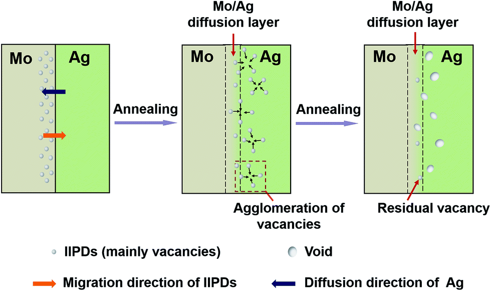
It can be seen from Table 1, with the increase of annealing temperature, the S-parameter values of the peaks decrease from 0.4635 to 0.4501 and the corresponding depth of the peaks decreases from 155 nm to 78 nm. The fact that the thickness of the vapor-deposited Ag layer is 100 nm means that the depths at 155 nm and 78 nm are located in the Mo and Ag layer, respectively. The VEPAS tests and the migration process of the IIPDs in the Mo/Ag laminated samples when the annealing temperature rises from 300 to 700 °C can be shown in a schematic diagram (see Fig. 5).
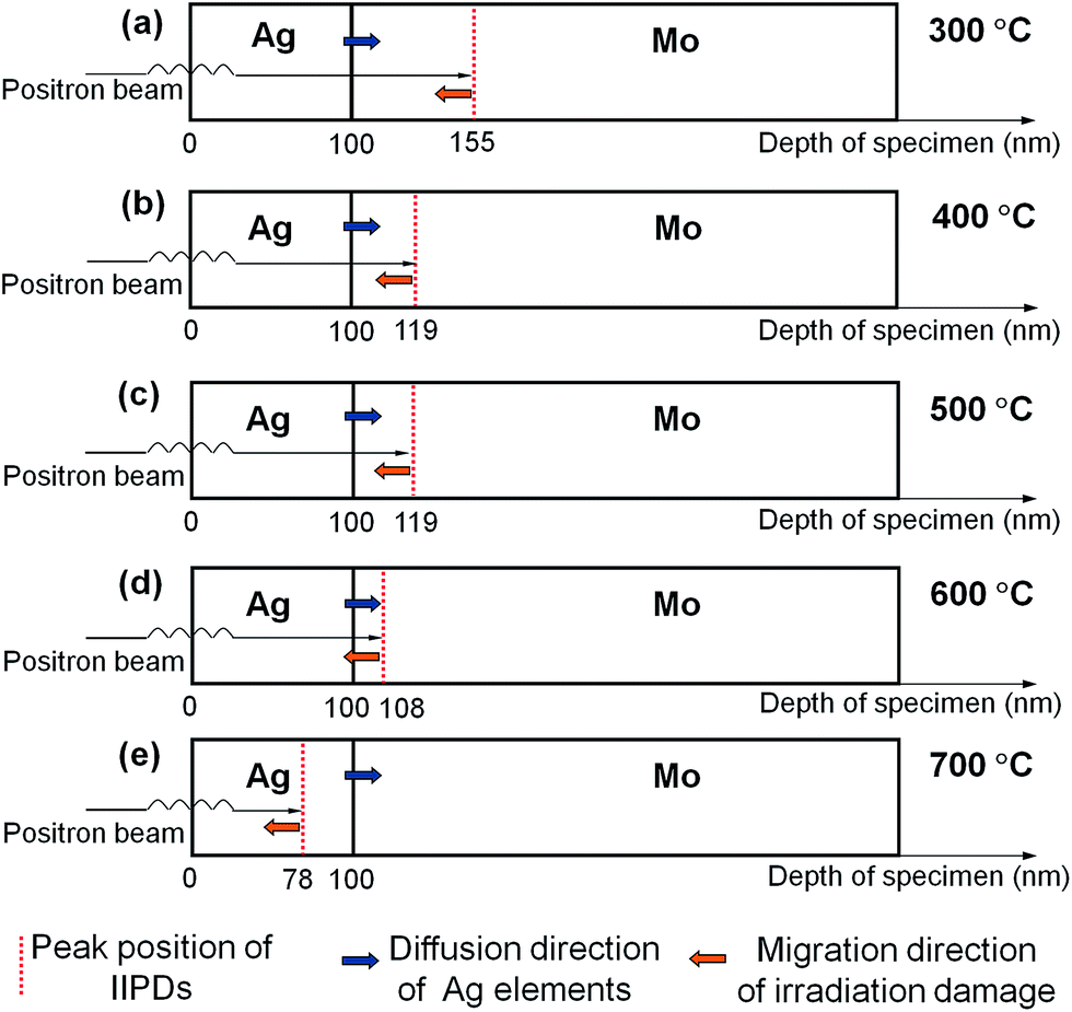 | ||
| Fig. 5 Schematic view of the migration process of the IIPDs in the Mo/Ag laminated samples when the annealing temperature rise from 300 to 700 °C. (a) 300 °C, (b) 400 °C. (c) 500 °C, (d) 600 °C, (e) 700 °C. Positron beams from the VEPAS come into contact with the IIPDs in the annealed samples and annihilate, giving the information of the peak position of the IIPDs in the samples. | ||
According to the analysis above, it can be concluded that the IIPDs migrate toward the Ag layer, which is in the direction opposite to the Ag diffusion. The corresponding migration distance is roughly equal to 77 nm (155–78 = 77 nm).
Furthermore, according to the data in Table 1, the diffusion energy barrier (Ea) of the IIPDs in the experiments can be calculated as follows:26
| L2 = 6Dt | (1) |
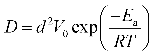 | (2) |
 , where a is the lattice constant of the Mo or Ag, V0 is vibration frequency of approximately 1012 s−1 and T is the annealing temperature. From the above equations, we can estimate Ea to be 1.6383, 1.8817, 2.0850 and 1.975 eV at 400, 500, 600 and 700 °C, respectively. Such energy barriers indicate that the migrating IIPDs are vacancies.27
Fig. 4b also shows that, for the Mo/Ag laminated sample annealed at 800 °C, the S values at each depth are not very different from each other. This may be caused by the fact that the migrated vacancies are aggregated into scattered large voids. When the annealing temperature is 900 °C, the line shape of the S curve of the laminated sample is close to that of pre-annealed pure Mo, indicating that the defects and crystals in the sample are being recovered.
3.4. Mechanism of the diffusion induced by irradiation-induced point defects
Fig. 6 shows the drift-corrected spectrum image scanning and the EDX line-scanning profile along the red solid line drawn in Fig. 6a, respectively. According to Fig. 6b, it can be seen that a Mo/Ag diffusion layer with a 79 nm thickness has been formed. The fact means that the diffusion distance of the Ag elements in the Mo layer is about 79 nm, which agrees well with the migration distance (about 77 nm) of the IIPDs as concluded from Table 1.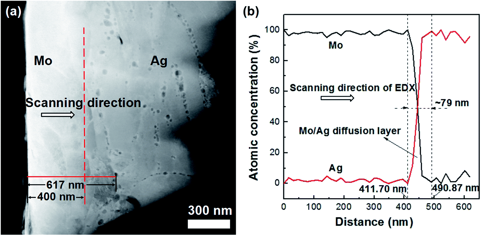 | ||
| Fig. 6 EDX line-scanning results of the cross-section of the Mo/Ag laminated sample annealed at 800 °C for 4 h. (a) Drift-corrected spectrum image scanning, (b) EDX line-scanning profile along the red line marked in (a). | ||
According to the above results and considering that the directions of Ag diffusion and the migration of the IIPDs are opposite, it can be concluded that the IIPDs can indeed induce the diffusion of the Ag elements from the outer layer into the Mo layer during high-temperature annealing, and the corresponding diffusion mechanism is most likely the vacancy-assisted mechanism.8,9
3.5. Further evidence for the vacancy mechanism
Since the diffusion occurs by the vacancy-assisted mechanism and the IIPDs (mainly vacancies) migrate toward the Ag layer, the Kirkendall effect should be observed in the Mo/Ag laminated sample. In other words, if the Kirkendall voids28–30 are observed in the Ag layer, the vacancy mechanism presented in Section 3.4 will be further proven.Fig. 7 shows the TEM images of the cross-section of the Mo/Ag laminated sample annealed at 800 °C for 4 h, which were obtained by a Tecanai G2 F20 S-Twin TEM. According to Fig. 7a and b, voids in the size range 20–30 nm are indeed found in the Ag layer and the Mo/Ag diffusion layer, while no voids are found in the Mo layer.
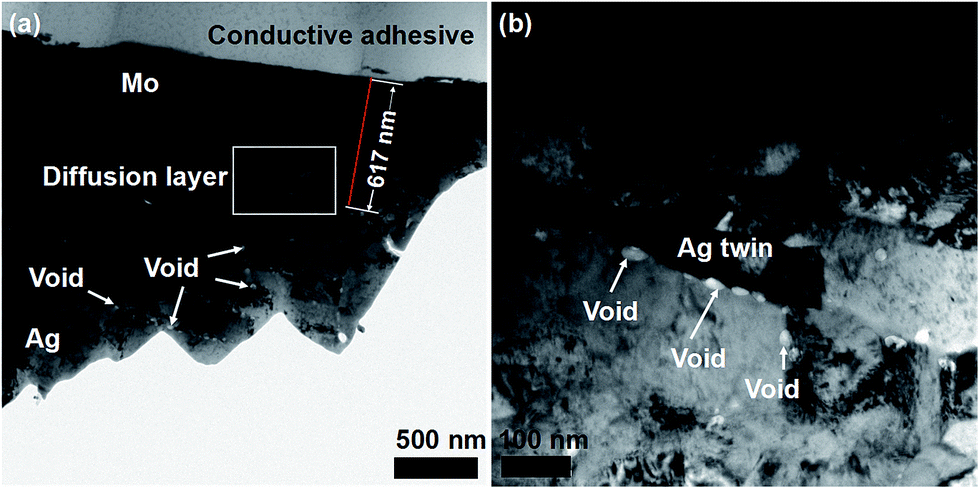 | ||
| Fig. 7 TEM obtained with a Tecanai G2 F20 S-Twin TEM for the Mo/Ag laminated sample annealed at 800 °C for 4 h. (a) TEM image, (b) magnified image of the region marked with a white rectangular frame in (a). | ||
In order to determine that those voids are aggregated by the migrated IIPDs, a new Pt/Ag laminated sample was prepared through evaporating Ag onto a platinum substrate that has not been damaged by irradiation, and a sequential annealing at 800 °C for 4 h. Fig. 8 is the TEM image of the Pt/Ag laminated sample, where the inset is the electron diffraction pattern of the Ag layer. It can be seen from Fig. 8 that annealing silver twins have formed in the Ag layer and there are no voids to be found both in the twin boundaries and the silver matrix. Comparing Fig. 7 with Fig. 8, it can be concluded that the voids in Fig. 8 are aggregated by the migrated IIPDs.31 The result means that the voids in Fig. 7 are the Kirkendall voids, which further proves that the mechanism of the diffusion induced by IIPDs is the vacancy-assisted mechanism. Since the migrating IIPDs are vacancies (see Section 3.3), the forming process of the Kirkendall voids can be described in Fig. 9.
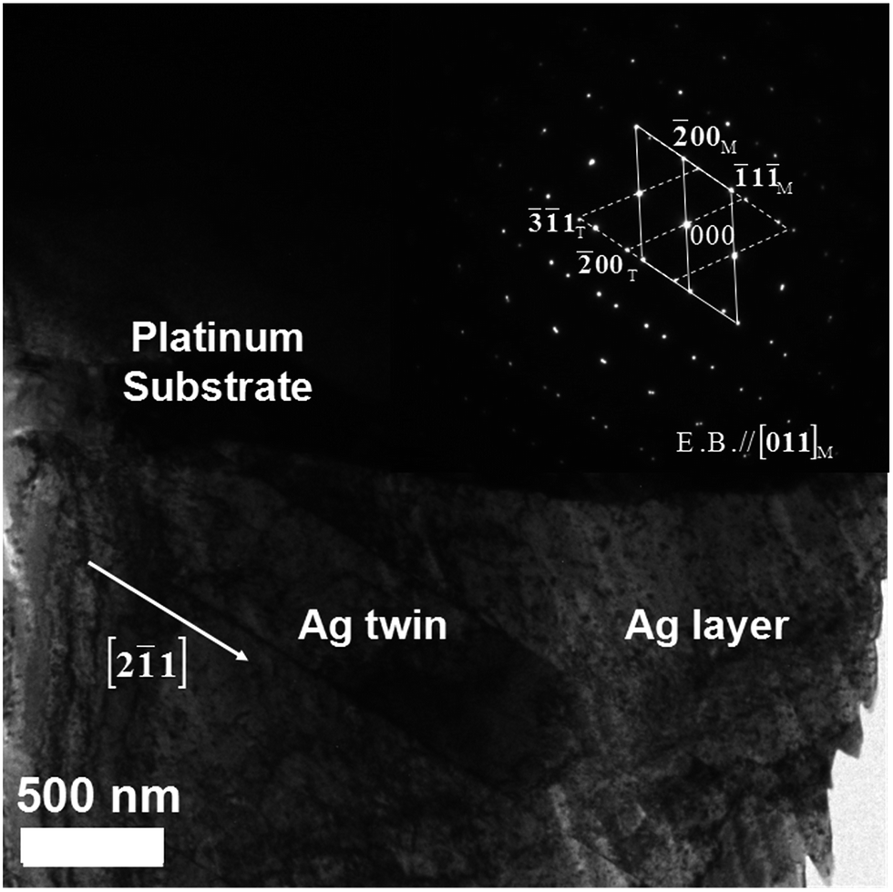 | ||
| Fig. 8 TEM image and electron diffraction pattern of the Pt/Ag laminated sample prepared though evaporating Ag onto a platinum substrate that has not been damaged by irradiation, and a sequential annealing at 800 °C for 4 h. | ||
 | ||
| Fig. 9 Schematic view of the forming process of the Kirkendall voids in the Mo/Ag laminated sample. | ||
In addition, since the IIPDs are just caused in the Mo through ion implantation, the Kirkendall voids observed in the Ag layer prove the conclusion: the IIPDs migrate toward the Ag layer, which is drawn through the VEPAS tests in Section 3.3.
Lastly, the discovery of these voids in the size range 20–30 nm can also verify the analysis for the VEPAS results of the Mo/Ag sample annealed at 800 °C in Section 3.3.
3.6. Application and prospect
The diffusion alloying method based on the induction of diffusion by IIPDs described in this paper is very suitable to realize alloying at the interface between the immiscible metals. So the method can be used to prepare LMCs based on immiscible metals, including Mo–Ag, W–Ag, Mo–Cu, W–Cu, Nb–Cu, Cu–Ta and Al–Be metals. We have successfully prepared Mo/Ag LMCs by using the method without using any metal interlayer.15 The obtained Mo/Ag LMCs have the characteristics of atomic oxygen resistance, high interfacial bonding strength, low thermal expansion, high conductivity and good weld ability, which can be used for the interconnectors of spacecraft solar arrays.Although ion implantation technology is used to cause IIPDs in metals in this research, we believe that the method of irradiation should not be limited to ion implantation technology. Other irradiation methods should also be included, e.g., nuclear irradiation and electron beam irradiation, which need to be validated in the future work. In addition, the method of evaporation plating an Ag layer on the Mo sheets can also be replaced by the superimposition of an Ag foil (or sheet).
4. Conclusions
In conclusion, IIPDs can be used to induce diffusion and construct the metallurgical interface directly between immiscible metals. Since the importance of Mo/Ag LMCs in aerospace, the Mo–Ag immiscible system is used as a research object in this paper. The process of induction of the diffusion consists of three steps: Mo is damaged by ion implantation, an Ag layer is evaporated on the damaged Mo and high temperature annealing is performed on the Mo/Ag laminated sample. Through the induction, the Ag elements from the vapor-plating Ag layer successfully diffuse into the Mo layer. The intrinsic mechanism for this diffusion induced by IIPDs in the immiscible system is the vacancy-assisted mechanism presented in solid-solution systems. The evidences for the vacancy mechanism are as follows: (1) the directional migrations of IIPDs take place along with the diffusion of Ag elements; (2) the migrating IIPDs are vacancies; (3) the migration direction of the IIPDs is opposite to that of the Ag diffusion; (4) the migration distance of the IIPDs (∼77 nm) agrees well with the diffusion distance of the Ag elements (∼79 nm); and (5) the Kirkendall effect arise and the Kirkendall voids are found in the Mo/Ag laminated samples. Through the induction of the above diffusion, a metallurgical interface is successfully constructed between immiscible Mo and Ag.This work provides a method to induce diffusion in immiscible systems, including Mo–Ag, W–Ag, Mo–Cu, W–Cu, Nb–Cu, Cu–Ta and Al–Be alloys. The method can be used in some industrial applications such as laminated metal composites (LMCs), metal connections and metallic cementation based on the immiscible metals.
Conflicts of interest
There are no conflicts to declare.Acknowledgements
This work is supported by the National Natural Science Foundation of China (51171128 and 51471114), and the Science and Technology Support Project of Tianjin City (11ZCKFGX03800).References
- A. de Rooij, Noordwijk, ESA WPP, 1995, vol. 77, pp. 341–353 Search PubMed.
- E. J. Mittemeijer, Fundamentals of Materials Science, Springer, Berlin, 2005, p. 339 Search PubMed.
- Y. A. Du, R. G. Hennig and J. W. Wilkins, Phys. Rev. B: Condens. Matter Mater. Phys., 2006, 73, 245203 CrossRef.
- B. S. Cao and M. K. Lei, Phys. Rev. B: Condens. Matter Mater. Phys., 2007, 76, 212301 CrossRef.
- B. Ziebarth, M. Mrovec, C. Elsässer and P. Gumbsch, Phys. Rev. B: Condens. Matter Mater. Phys., 2015, 92, 115309 CrossRef.
- K. C. Pandey, Phys. Rev. Lett., 1986, 57, 2287–2290 CrossRef CAS PubMed.
- P. O. Bugnion and G. J. Conduit, Phys. Rev. A: At., Mol., Opt. Phys., 2013, 88, 013601 CrossRef.
- D. Srivastava, M. Menon, C. Daraio, S. Jin, B. Sadanadan and A. M. Rao, Phys. Rev. B: Condens. Matter Mater. Phys., 2004, 69, 153414 CrossRef.
- O. U. Uche, D. Perez, A. F. Voter and J. C. Hamilton, Phys. Rev. Lett., 2009, 103, 046101 CrossRef CAS PubMed.
- E. Ma, Prog. Mater. Sci., 2005, 50, 413–509 CrossRef CAS.
- S. Odunuga, Y. Li, P. Krasnochtchekov, P. Bellon and R. S. Averback, Phys. Rev. Lett., 2005, 95, 045901 CrossRef CAS PubMed.
- P. Zhao, S. Wang, S. B. Guo, Y. X. Chen, Y. H. Ling and J. T. Li, Mater. Des., 2012, 42, 21–24 CrossRef CAS.
- Y. Itoh, M. Takahashi and H. Takano, Fusion Eng. Des., 1996, 31, 279–289 CrossRef CAS.
- Y. Di, M. A. Kirk, P. M. Baldo, J. Rest, A. M. Yacout and Z. Z. Insepov, J. Nucl. Mater., 2013, 437, 240–249 CrossRef.
- Y. Huang, D. Y. Kong, F. He and Y. L. Wang, Acta Metall. Sin., 2012, 48, 1253–1259 CrossRef CAS.
- Y. Z. Liu, X. B. Hu, S. J. Zheng, Y. L. Zhu, H. Wei and X. L. Ma, Mater. Des., 2015, 80, 63–69 CrossRef CAS.
- L. J. Chen, Mater. Sci. Eng., R, 2000, 29, 115–152 CrossRef.
- I. Procházka, J. Čížek, V. Havránek and W. Anwand, J. Alloys Compd., 2015, 645, S69–S71 CrossRef.
- P. Horodek and V. A. Skuratov, Surf. Coat. Technol., 2016, 296, 65–68 CrossRef CAS.
- C. L. Dube, P. K. Kulriya, D. Dutta, P. K. Pujari, Y. Patil, M. Mehta, P. Patel and S. S. Khirwadkar, J. Nucl. Mater., 2015, 467, 406–412 CrossRef CAS.
- P. Horodek, J. Dryzek and V. A. Skuratov, Radiat. Phys. Chem., 2016, 122, 60–65 CrossRef CAS.
- M. Clement, J. M. M. De Nijs, P. Balk, H. Schut and A. Van Veen, J. Appl. Phycol., 1996, 79, 9029 CrossRef CAS.
- Y. Geng, T. Ablekim, M. A. Koten, M. Weber, K. Lynn and J. E. Shield, J. Alloys Compd., 2015, 633, 250–255 CrossRef CAS.
- U. Myler, R. D. Goldberg, A. P. Knights, D. W. Lawther and P. J. Simpson, Appl. Phys. Lett., 1996, 69, 3333 CrossRef CAS.
- M. Hakala, M. J. Puska and R. M. Nieminen, Phys. Rev. B, 1998, 57, 7621–7627 CrossRef CAS.
- E. J. Mittemeijer, Fundamentals of Materials Science, Springer, Berlin, 2005, p. 343 Search PubMed.
- L. S. Shun, C. Z. Bi, W. Y. Wang, A. J. Ross, X. L. Liu, Y. J. Hu, H. Z. Fang, Y. Wang and Z. K. Liu, Acta Mater., 2016, 109, 128–141 CrossRef.
- H. J. Fan, U. Gosele and M. Zacharias, Small, 2007, 3, 1660–1671 CrossRef CAS PubMed.
- H. Mitsuyasu, Y. Nonaka and K. Eguchi, Solid State Ionics, 1998, 113, 279–284 CrossRef.
- X. S. Zhou, Y. T. Dong, C. X. Liu, Y. C. Liu, L. M. Yu, J. G. Chen, H. J. Li and J. G. Yang, Mater. Des., 2015, 88, 1321–1325 CrossRef CAS.
- P. G. Coleman, R. E. Harding, G. Davies, J. Tan and J. Wong-Leung, J. Mater. Sci.: Mater. Electron., 2007, 18, 695–700 CrossRef CAS.
| This journal is © The Royal Society of Chemistry 2017 |