DOI:
10.1039/C7RA11058H
(Paper)
RSC Adv., 2017,
7, 55471-55481
Compositional effect on the fabrication of AgxPd1−x alloy nanoparticles on c-plane sapphire at distinctive stages of the solid-state-dewetting of bimetallic thin films†
Received
8th October 2017
, Accepted 1st December 2017
First published on 7th December 2017
Abstract
Bimetallic nanoparticles (BMNPs) exhibit composition, dimension and configuration dependent optical, catalytic and magnetic properties, which can make them promising candidates for various applications. In this paper, the AgxPd1−x bilayer composition effect, i.e. Ag0.75Pd0.25, Ag0.50Pd0.50 and Ag0.25Pd0.75, on the evolution of AgxPd1−x BMNPs is thoroughly investigated on c-plane sapphire by the control of annealing temperature, duration and deposition thickness. Bimetallic nanoparticles of various dimensions and configurations are fabricated at different dewetting stages by the thermal activation, diffusion and inter-mixing of Ag–Pd adatoms with respect to the growth conditions. With elevated annealing temperature, the gradual transition from voids to nanoclusters and individual BMNPs is demonstrated based on the surface and interface energy minimization and Volmer–Weber growth model. Owing to the high diffusivity of Ag atoms, the bilayers with the higher Ag component show improved dewetting at relatively low temperature whereas the high Pd composition set shows an increased stability against dewetting. Meanwhile, the transition of BMNPs from connected to individual and compact spherical configuration is witnessed along with extended annealing duration. At the same time, a significant dimensional expansion of NPs is achieved with increased deposition thickness. On the other hand, the Ag concentration from BMNPs is reduced due to sublimation at high temperature, which causes overall size attenuation. Moreover, the fabricated AgxPd1−x BMNPs are characterized based on their reflectance spectra and the evolution of their absorption band, peak formation and their shifts are correlated with the dynamic surface plasmon resonance of AgxPd1−x BMNPs based on the surface morphology.
Introduction
Recently, nanoparticles (NPs) have been widely adopted in various applications including fuel-cells, water splitting, pollution treatment, energy harvesting and sensing owing to their physical, chemical, optical and catalytic properties depending on their size, density and configuration.1–5 Bimetallic nanoparticles (BMNPs) including both elements in a nanoparticle are of particular interest because they can demonstrate additional functionality, tunability and device performance.6–8 For example, as compared to monometallic catalytic systems, Pd-based BMNPs showed a profound enhancement in catalytic activity, selectivity and stabilities for various reactions such as CO oxidation and hydrogenation of hydrocarbons.9,10 In addition, owing to the structure and element dependent localized surface plasmon resonance (LSPR), the BMNPs can be applied in various optoelectronic devices to improve the optical output, conversion efficiency and detection sensitivity.11–15 At the same time, the monometallic Ag and Pd NPs individually have been important materials in optical, plasmonic and catalytic applications.16,17 At this stage, the idea of combining both Ag and Pd atoms in a single nanostructure can further extend their applicability and thus the fabrication of bimetallic AgxPd1−x nanostructures by controlling their morphology and elemental composition can be promising approach to explore the functionality and usability for the related and novel applications. However, the systematic study of AgxPd1−x BMNP fabrication especially through the physical vapor deposition is still unexplored in terms of both growth mechanism and optical properties. Thus, in this work, the AgxPd1−x BMNPs are fabricated through the dewetting of Ag/Pd bilayers on c-plane sapphire. By the control of annealing temperature, duration and deposition thickness and bilayer composition, various AgxPd1−x BMNPs are fabricated and described based on the dewetting rate, surface and interface diffusion, surface energy minimization, Volmer–Weber growth model and Ag sublimation. The surface plasmon effect of AgxPd1−x BMNPs is probed by the reflectance spectra, such as the formation of constant UV-peaks, wide visible dips and varying NIR peaks along with the morphology evolution.
Experimental section
The substrates utilized in this work were ∼430 μm-thick c-plane sapphire wafers with an off-axis less than 0.1° (iNexus Inc., South Korea). The 6 × 6 mm2 squared samples were dice-prepared and then degassed at 600 °C for 15 min under the vacuum 1.0 × 10⁻⁴ Torr in order to remove the various particulates, oxides and trapped gases. The AFM morphology of bare sapphire after the degassing can be referred in Fig. S1 (ESI†) with the top- and side-views. The bimetallic layers were deposited by a plasma-assisted sputtering with an ionization current of 3 mA and rate of ∼0.05 nm s−1 under 1 × 10⁻¹ Torr. The Ag and Pd targets used in this study were with 99.999% purity. The deposition thickness of metallic layers was controlled by the deposition duration. In the annealing temperature investigation, various thickness of Ag and Pd layers were sequentially deposited to produce the bilayers of distinct compositions: Ag0.75Pd0.25, Ag0.50Pd0.50 and Ag0.25Pd0.75 (AgxPd1−x: x is the composition in % for a total thickness of 15 nm). More specifically, with the 15 nm total thickness, the Ag0.75Pd0.25 indicates the 11.25 nm of Ag film and 3.75 nm of Pd film in the Ag/Pd bilayer. Similarly, the Ag0.50Pd0.50 composition means 7.5 nm of Ag film and 7.5 nm of Pd film whereas the Ag0.25Pd0.75 denotes the 3.75 nm of Ag film and 11.25 nm of Pd film. Meanwhile, in the study of deposition thickness and annealing duration, the Pd layers were deposited first and then Ag layers were added with the compositions of Pd0.25Ag0.75, Pd0.50Ag0.50 and Pd0.75Ag0.25. For deposition thickness control set, 2 to 30 nm total thickness was varied at constant annealing condition whereas 10 nm total thickness samples were prepared for the duration variation set. The deposited samples were mounted on an Inconel holder and transferred to the annealing chamber for the following annealing process. The samples were then heated with a ramp rate of 4 °C s−1 under the vacuum below 1 × 10⁻⁴ Torr. For the temperature investigation, the target temperature was varied between 400 and 800 °C and an equal duration of 120 s was applied for all the samples. For the deposition thickness and annealing duration investigations, the target temperatures were fixed at 650 °C and an annealing duration of 120 s was equally applied. To finish the growth, heating system was turned off and samples were kept under vaccum until the temperature reached to the ambinet. The morphology of BMNPs were characterized by an atomic force microscope (AFM), XE-70, Park Systems, South Korea and a scanning electron microscope (SEM), CX-200, COXEM, South Korea. The AFM probes possess a length of 125 μm, a width of 30 μm, and the typical height and radius of the tip were 17 μm and <10 nm respectively, working under the non-contact mode. The elemental analysis including spectra and spectral maps were acquired by an energy-dispersive X-ray spectroscope (EDS), Noran System 7, Thermo Fisher, USA. The reflectance spectra were obtained by the UNNIRAM II system, UniNanoTech, South Korea. The reflectance spectra were obtained with the light sources of halogen (450 nm ≤ λ ≤ 1100 nm) and deuterium (300 nm ≤ λ ≤ 450 nm).
Result and discussion
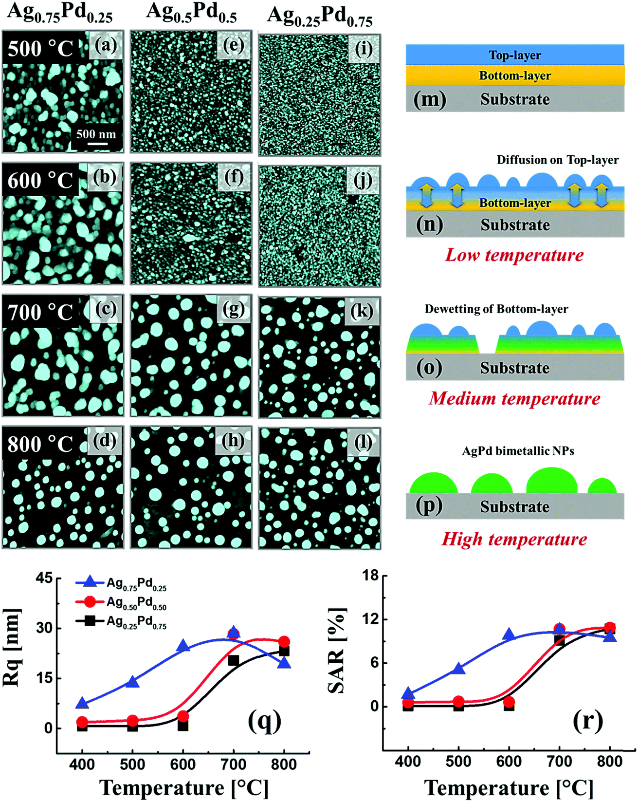
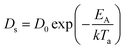
Fig. 1 shows the overall evolution process of Ag–Pd bimetallic nanoparticles (BMNPs) induced by the control of annealing temperature (Ta) between 500 and 800 °C for 120 s. The AFM top-views of 3 × 3 μm2 in Fig. 1(a)–(l) present the three distinct bilayer composition: Ag0.75Pd0.25, Ag0.50Pd0.50 and Ag0.25Pd0.75 (Pd being on top) and the schematic diagrams in Fig. 1(m)–(p) illustrate the BMNP evolution process. Line-profiles of specific samples are provided in Fig. S3.† In general, the bimetallic layers were gradually dewetted into the isolated Ag–Pd BMNPs along with the increased Ta and a sharp distinction in the dewetting process was observed for distinct composition. In case of monometallic film, the dewetting sequence of films follow series of morphological stages such as nucleation of voids and growth, and formation of isolated nanostructures and growth,18,19 which are similar to the dewetting sequence of bilayer films. In the dewetting of monometallic films, the main governing parameter is the surface diffusion, activation energy and surface energy of the metal films.20–22 Since, the surface energies of Ag and Pd are 1065 and 1808 mJ m−2 respectively23 and the activation energies for Ag and Pd are 200 and 203 kJ mol−1 respectively as reported earlier.24 Thus, the surface diffusion Pd and Ag adatoms are different, in which the surface diffusion of Ag adatoms are higher than that of Pd atoms. Meanwhile, the formation of BMNPs can be commenced by the solid-state-dewetting of bilayers by means of the surface diffusion as well as inter-diffusion of metal atoms.25,26 Along with the thermal energy applied, metallic atoms start to diffuse on the surface and at the Ag/Pd interface (inter-mixing) and the diffusion coefficient Ds of atom can be related to the Ta as | |
 | (1) |
where the D0 is the pre-exponential factor of surface diffusion coefficient, EA is activation energy of atoms and k is Boltzmann constant. The D0 and EA are material constants and thus, Ds is mainly related with the.Ta27 Meanwhile, the sputter-deposited metallic films generally possess numerous atomic vacancies, defects, grain boundaries as well as step/kinks, which offer low energy sites that triger the dewetting process by the void/pinholes nucleation.26 After the formation of voids, they can grow by absorbing more vacancies or colliding with nearby voids and the growth rate of voids rvoid can be expressed as | |
 | (2) |
where the t is the thickness of a layer. In eqn (2), the first term Ds/Ta indicates the surface diffusion effect on the.rvoid28 As seen in eqn (1), the Ds can be exponentially increased with the increased Ta and thus the void growth also can be accelerated with temperature. At the same time, along with the thermal energy applied, the interfacial diffusion of Ag atoms towards Pd layers and Pd atoms towards Ag layers can occur and the inter-mixed layer can be enlarged as illustrated in Fig. 1(n). Along with the increased Ta, the voids can keep growing larger, exposing the substrate surface due to the surface capillary forces around the voids rims28 as seen in Fig. 1(o). Finally, the void rims can be fragmented leading to the formation of individual nanostructures due to the energy perturbations such as Rayleigh instability.15,28,29 On the other hand, the binding energy between metallic atoms can be greater than that with substrate and thus, the growth can proceed to the 3-D island formation based on the Volmer–Weber growth model as seen in Fig. 1(p).30,31 Along with the dewetting of bilayer films, the elemental distribution of Ag and Pd atoms in isolated NPs can be improved toward the improved homogeneity due to the enhanced inter-diffusion with increased Ta.32,33 In the isolated Ag–Pd NPs, the Ag and Pd are completely miscible at any proportion due to the same crystallographic structure with the similar lattice parameters and no miscibility gap at any composition based on the Ag–Pd alloy phase diagram.34 In contrast to the monometallic dewetting, the bilayer dewetting can be slightly different and indeed somewhat more complex due to the various factors such as different diffusivity, surface energies, surface segregation, alloying, lattice mismatch and stress generation–relaxation between constituent materials, etc. Therefore, the dewetting extent can be significantly varied even at identical growth conditions such as annealing temperature, thickness and duration by the alteration of composition or sequence of individual atomic species. Initially, the sputtering deposited atoms on substrate can under goes a series of kinetic process including the surface diffusslqion, nucleation of pinholes and voids.35,36 Depending on the bi-layer composition, the growth at relatively lower temperature range can be regarded as a heterogeneous dewetting as the dewetting can be initiated by the diffusion of Ag atoms at the low energy sites such as defect and steps.37,38 As the temperature was increased more like homogeneous dewetting can be observed along with the full alloying of elements. The Ag–Pd bilayer film deposition on sapphire (0001) have a perforation morphology along with the formation of small pinholes. After the annealing at 500 °C for the Ag0.75Pd0.25 set as presented in the left-first column, the formation of voids and agglomeration of nanoclusters was already started and the alloy NPs were gradually improved in shape along with the elevated Ta. Whereas with the increased Pd component, small voids were seen up to 600 °C and abrupt surface morphology transformation occurred at 700 °C for the Ag0.50Pd0.50 and Ag0.25Pd0.75 sets as shown in second and third columns. From the previous studies,39,40 the monometallic Ag layers were well dewetted even at the low Ta of 400 °C and formed definite NPs whereas the Pd showed visible dewetting only above 600 °C, which was due to the lower diffusivity and higher surface energy of Pd. Thus, at relatively lower temperatures, the Pd films can induce the thermal stability against the dewetting, namely the lower the bilayers dewetting, which can be clearly seen with in the first two columns with the thicker the Pd layers. In the case of thinner Pd top-layer, owing to the higher diffusivity of the Ag adatoms, it can diffuse through the voids resulting in the extensive void growth and formation of nanoclusters at relatively lower Ta. However, at higher Ta, the surface and interface diffusion can be both sufficient and thus, the formation of isolated NPs was equally observed in all bilayer composition. With the further enhanced surface diffusion at 800 °C, NPs were developed into a spherical configuration due to the isotropic surface energy distribution of alloy NPs. The overall dewetting process can be driven by the surface and interface energy minimization of the thermodynamic system. In addition, the morphology evolution was studied in terms of RMS roughness (Rq) and surface area ratio (SAR) as displayed in Fig. 1(q) and (r). Specifically, the Rq was increased along with the development of partially dewetted clusters, irregular NPs and isolated alloy NPs as the surface height was gradually increased as discussed above. A similar trend was observed for the SAR. In the case of un-dewetted layer-like structures, the Rq and SAR were lower and were not changed significancy. In addition, at high Ta, the size of alloy NPs were decreased as suggested by the decrease in the Rq and SAR, which can be due to the sublimation of Ag atoms. As a material with a low melting point (961.8 °C), Ag undergoes a considerable sublimation at increased Ta as expressed by the relation, sublimation rate | |
 | (3) |
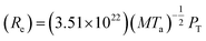
where, the M is the molecular weight of Ag and PT is the vapor pressure of Ag at specific Ta.41 As the increase of PT is exponential with the Ta, the Re can be significantly increased with Ta. As evidenced by the EDS spectra in Fig. 2(d)–(f), significant attenuation of Ag Lα1 peak was observed between 600 and 800 °C while a Pd Lα1 peak exhibited a constant intensity, suggesting no sublimation of Pd. As shown in the plot, the counts of the Ag Lα1 peak are generally higher than Pd Lα1 peak owing to the higher atomic number of Ag. The enhanced diffusion along with the sublimation of Ag atoms can induce a significant modulation in NP configuration. The contact angle ‘θ’ for the alloy NPs at 700 and 800 °C were measured for all compositions by the measurement of the average height and diameter as displayed in the Fig. 2(a)–(c). As clearly seen in the height and diameter histograms, the diameter of alloy NPs was decreased for all three sets due to the Ag sublimation loss. In terms of height, there was slight decrease in all three sets from 700 to 800 °C. As a consequence, the θ was increased for all three sets. In specific, the θ for Ag0.75Pd0.25 set was significantly increased whereas other compositions showed slight increase because of the size (diameter) reduction by the Ag sublimation.
 |
| | Fig. 1 Evolution of Ag–Pd bimetallic nanostructures on sapphire (0001) by the control of annealing temperature between 500 and 800 °C for 120 s with the deposition thickness of 15 nm with distinct bilayer composition as labelled. (a)–(l) AFM top-views of 3 × 3 μm2. (m)–(p) Schematic diagrams of bimetallic nanoparticle formation. (q) & (r) Root mean squared roughness (Rq) and surface area ratio (SAR) as a function of annealing temperature. | |
 |
| | Fig. 2 Morphological and elemental analysis of the Ag–Pd bimetallic nanostructures, fabricated at different annealing temperature. (a) Ag–Pd nanoparticle fabricated at 800 °C for 120 s with the bilayer composition of Ag0.5Pd0.5. (b) Average diameter, height and dewetting angle (θ) for the various Ag–Pd nanoparticles fabricated at 700 and 800 °C. Error bars for the diameter, height and dewetting angle are ± 5%. (c) Schematic diagrams of the control of dewetting angle. (d)–(e) EDS spectra of the Ag0.75Pd0.25 and Ag0.25Pd0.75 samples fabricated at 500 and 800 °C. (f)–(h) EDS intensities of Ag Lα1 and Pd Lα1 plotted as functions of annealing temperature. | |
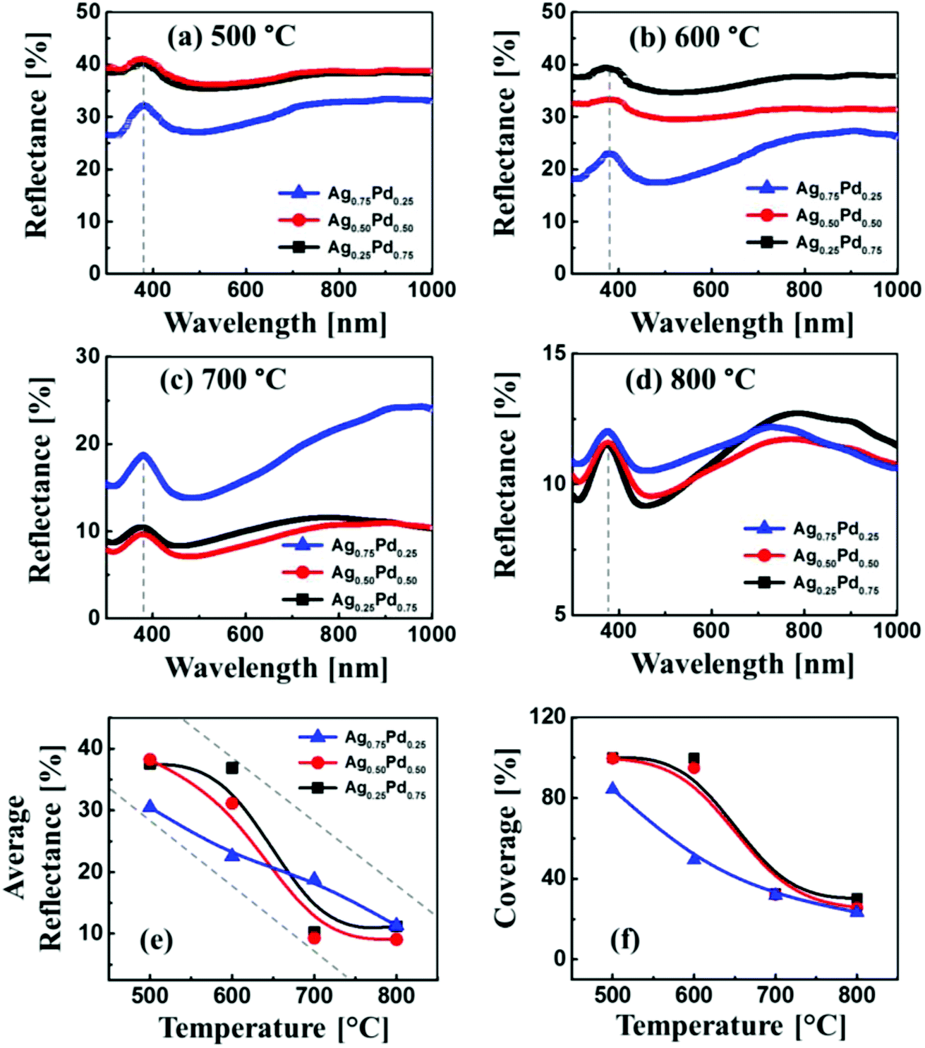
Fig. 3 shows the reflectance spectra of the Ag–Pd BMNPs, fabricated at various Ta with the different bilayer composition as labelled. Generally, all the Ag–Pd BMNPs showed a peak in UV region and dip in visible region corresponding to the surface plasmon resonance of the Ag–Pd alloy NPs.42 The monometallic Ag NPs exhibited a strong plasmon resonance band in the visible region while the monometallic Pd NPs have a weaker plasmon band.43,44 Particularly, the Ag NPs fabricated with the deposition amount below 15 nm exhibited the strong absorption dip and plasmon resonance band whereas the Pd NPs showed near-flat reflectance spectra over the VIS-IR range without the formation of specific absorption or reflectance bands. Thus, alloying Ag and Pd, i.e. fabrication of Ag–Pd BMNPs, can enhance the plasmonic properties as compared with the Pd NPs. In specific, the Ag–Pd BMNPs can have an intermediate frequency of plasmonic band, in which the intensity is lower than the monometallic Ag NPs but higher than monometallic Pd NPs. Furthermore, the intensity of absorption dip and plasmon resonance peak can be tunable by the control of elemental composition and morphology of the Ag–Pd BMNPs. As an example, the partially dewetted alloy nanostructures such as in case of Ag0.5Pd0.5 and Ag0.25Pd0.75 bilayer compositions, the peak intensity was quite weak. However, the intensity was gradually increased and the bandwidth of peaks was became narrower along with the annealing temperature likely due to the formation of well-structured isolated alloy NPs. On the other hand, the reflectance in the NIR region was gradually enhanced with the Ta, resulting in a NIR shoulder or broad peak. Furthermore, at an identical temperature, the peak intensity of samples with the high Ag component was higher, which can be related to the enhanced plasmon response of Ag NPs in UV-vis region.42 In terms of average reflectance as shown in Fig. 3(e), it was gradually suppressed along with the Ta for all bilayer composition while the trends was slightly varied for each composition due to the variation in the surface morphology of specific Ag–Pd nanostructures. Generally, as metallic layers possess higher reflectivity,45 the reflectance can be attenuated by the dewetting of bilayers along with the absorption or scattering enhancement of surface plasmon resonance of Ag–Pd nanostructures. As clearly seen in the average coverage plot of Ag–Pd nanostructures in Fig. 3(f), large similarity in two plots can be found: i.e. the higher surface coverage, the higher reflectance and vice versa.
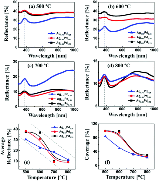 |
| | Fig. 3 (a)–(d) Reflectance spectra of the Ag–Pd nanostructures fabricated between 500 and 800 °C for 120 s with the deposition thickness of 15 nm and bilayers composition as labelled. (e) Average reflectance and (f) nanostructure coverage plots with respect to annealing temperature. | |
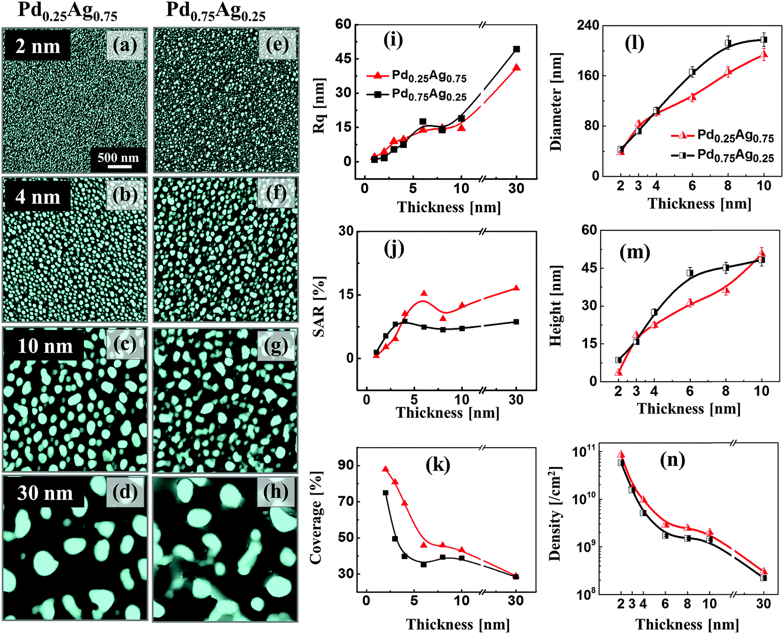
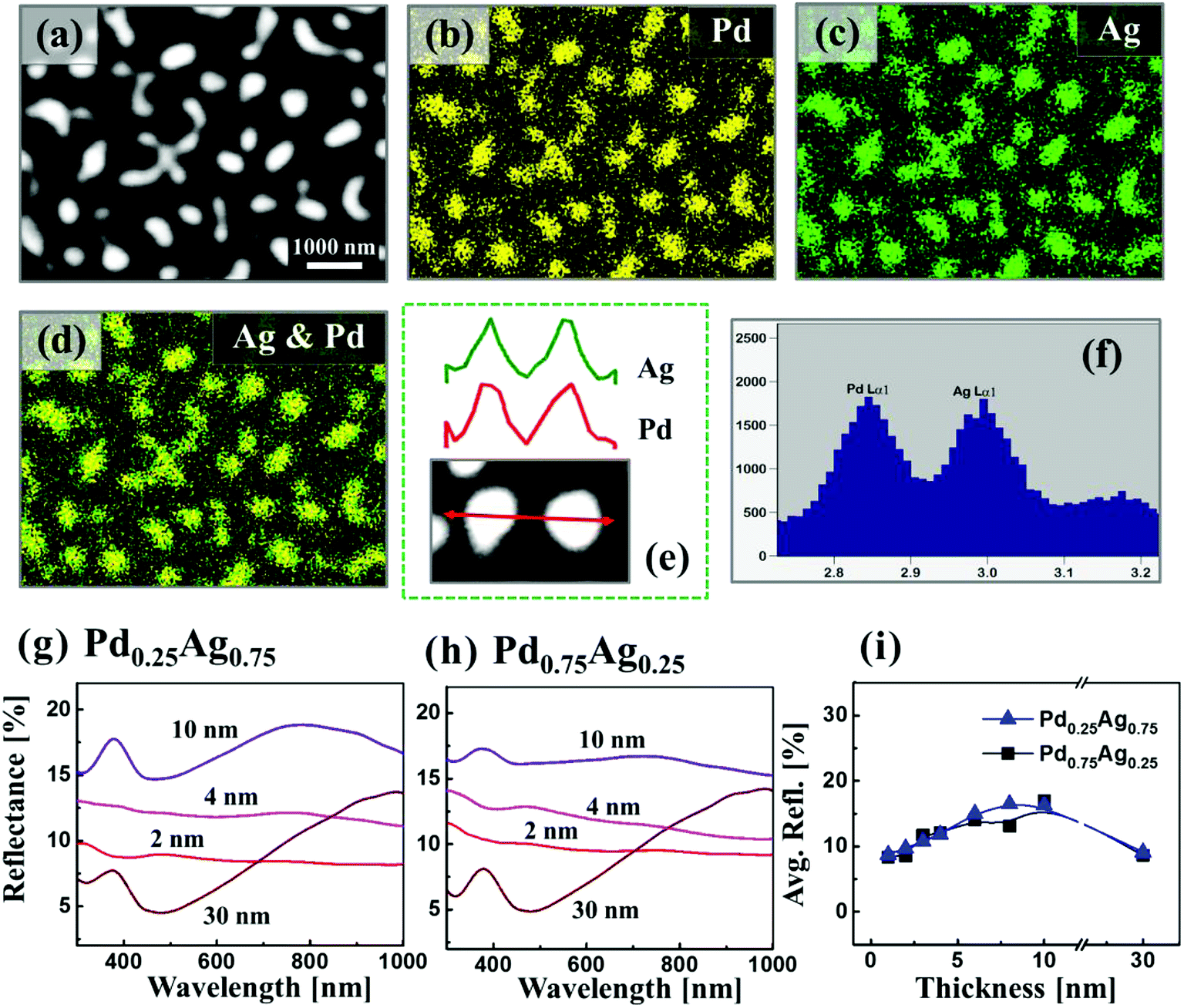
Fig. 4 presents the evolution of Ag–Pd bimetallic NPs by the control of deposition thickness between 2 and 30 nm at 650 °C for 120 s. In addition, the lineprofiles at specific locations are provided in the ESI Fig. S5–10.† The bilayers consist of Pd under layer and Ag top layer with variable individual composition (25% Pd in first column and 75% Pd in second column) as labelled. In this case, the Pd layer was deposited first to alter the dewetting process as compared to the temperature sets and hence the surface morphology of resulting nanostructures as the bilayers dewetting can be drastically varied by simply changing deposition order. In which, the change in binding energies with sapphire and surface diffusivities can play important role for dewetting process such that Pd-sapphire binding force is greater than Ag-sapphire and surface diffusivity of Ag is higher than Pd on sapphire.46,47 From the temperature sets and previous studies, the Ag and Pd films can attain sufficient dewetting around 650 °C, resulting in the formation of well-structured NPs.39,40 Thus, at this growth condition, sufficient surface diffusion and inter-mixing of Pd and Ag layers can be expected. At the same time, owing to the higher diffusivity of Ag on top, it can promote the overall dewetting of bilayers by the incorporation of Ag atoms into the Pd layers through the pinholes or viods. When the thermal energy for atoms diffusion is sufficient, once formed NPs can absorb the nearby diffusing adatoms through the self-assembly process resulting in the larger size with added materials.30,31 Therefore, at an identical growth environment, the NPs can grow sufficiently large possessing different surface configurations with the increased deposition thickness. In this case, the bimetallic NPs demonstrated a clear growing trend in size for both bilayer composition along with the increased deposition thickness. Specifically, in the first column with the Pd0.25Ag0.75 composition, the alloy NPs were mostly well-developed possessing spherical configuration whereas with the high Pd component (second column), slightly elongated NPs were obtained. This can be due to the lower diffusivity of thicker Pd, which tend to suppress the overall dewetting process as discussed. More specifically, tiny NPs were fabricated with relatively thinner thickness due to the enhanced diffusion of atoms and by increasing the bilayers thickness, the self-assembly of NPs was enhanced, resulting in larger size and lower density. Small bimetallic NPs normally fashioned in spherical configuration due to the isotropic surface energy distribution whereas larger NPs were irregular as they cannot sustaining the isotropy along with the coalescence of adjacent NPs. The surface morphology of NPs were studied in terms of Rq, SAR and coverage as shown in the Fig. 4(i)–(k). Generally, along with increased deposition thickness the Rq was gradually increased as the NP size was increased in both sets. However, the increase of SAR was interrupted or compensated between 6 and 30 nm due to the decrease in the NP density. In terms of the coverage in Fig. 4(k), a drastic decrease was observed with the deposition thickness between 2 and 6 nm and then it was slightly decreased up to 30 nm. In addition, the dimension were measured in terms of average diameter, height and density as shown in Fig. 4(l)–(n). Both the average height and diameter summary plots exhibited the increasing trends whereas density showed decreasing trends with respect to the bilayers thickness (specific numerical values and histograms are supplied in the ESI†). Furthermore, the alloy NPs, fabricated with higher Pd component possessed slightly larger dimension, which can be correlated to the Ag sublimation loss in Pd0.75Ag0.25 as compared to Pd0.25Ag0.75 bilayer composition. As displayed in Fig. 5(a)–(d), the elemental distribution of Pd and Ag was investigated for a typical sample with the Pd0.75Ag0.25 composition and 30 nm total thickness. The spectral images of Pd, Ag and Ag–Pd are in a good agreement with the NPs displayed in SEM image, suggesting an even distribution of both Ag and Pd atoms. Furthermore, the elemental line-profiles in Fig. 5(e) clearly depict the Ag and Pd elemental distribution in specific Ag–Pd bimetallic NPs. The corresponding Pd and Ag Lα1 peaks were observed at 2.84 and 2.98 keV respectively as seen in Fig. 5(f). About 3 times higher sensitivity was consistently observed for Ag in the system. The reflectance spectra of Ag–Pd BMNPs with various thickness are shown in Fig. 5(g)–(i). The reflectance spectra were significantly varied based on the evolution of various Ag–Pd alloy NPs along with the thickness control. For example, with the Pd0.25Ag0.75 composition, the tiny and compact NPs, i.e. 2 and 4 nm, demonstrated the uniform spectral response within 300 to 1000 nm wavelength, indicating a broadband absorption without the formation of obvious peaks or valleys due to the smaller dimension of NPs than that of incident wavelength.48 When the NPs became larger with the wider spacing, a sharp peak in UV region, wide dip in visible region and broad peak in the NIR region were gradually developed as seem in case of 10 nm thickness, suggesting the existence of surface plasmon resonance edge of the Ag–Pd alloy NPs.42 Meanwhile, with the increment of NPs size at higher deposition thickness, the NIR peak was red-shifted from ∼750 to ∼1000 nm whereas there was large attenuation of reflectance in visible region. Similarly, the Pd0.75Ag0.25 composition demonstrated comparable reflectance characteristic, however, the peak intensity was slightly weaker between 4–10 nm as compared to the previous set. As shown in Fig. 5(i), the average reflectance was gradually increased along with the size of Ag–Pd NPs up to 8 nm and showed a decreasing trend. This can be correlated to the decreased surface coverage with the larger spacing between the NPs.
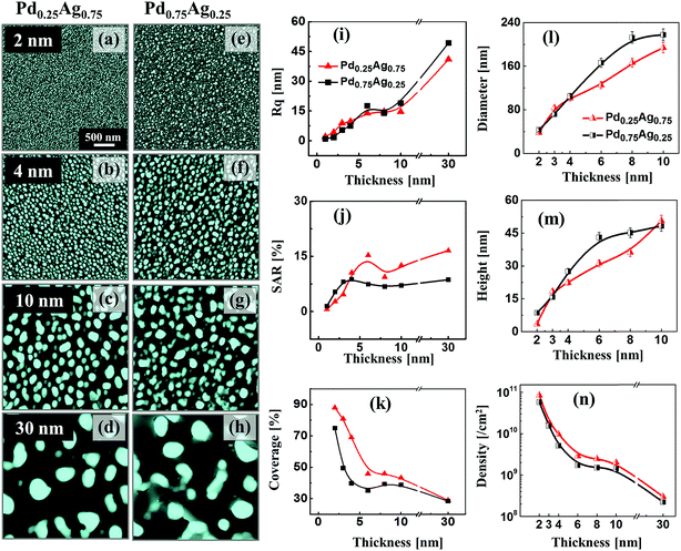 |
| | Fig. 4 Evolution of the Ag–Pd bimetallic nanostructures by the control of deposition thickness between 2 and 30 nm at different bilayer composition. The samples are fabricated at 650 °C for 120 s. (a)–(h) AFM top-views of 3 × 3 μm2. (i)–(k) Summary of Rq, SAR and coverage plot with respect to the deposition thicknesses. (l)–(n) Summary plots of average diameter, height and density. Error bars: ±5%. | |
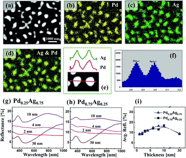 |
| | Fig. 5 EDS spectral map of the Ag–Pd alloy nanoparticles fabricated at 650 °C with the deposition thickness of 30 nm and Pd0.75Ag0.25 bilayer composition. (a) SEM image. (b) Pd, (c) Ag and (d) Pd–Ag phase mappings. (e) EDS line-profiles of two typical bimetallic nanoparticles. (f) Corresponding EDS spectrum for the sample. (g) and (h) Reflectance spectra of the Ag–Pd alloy nanostructures fabricated with the control of deposition thickness. (i) Summary plot of average reflectance with respect to thickness. | |
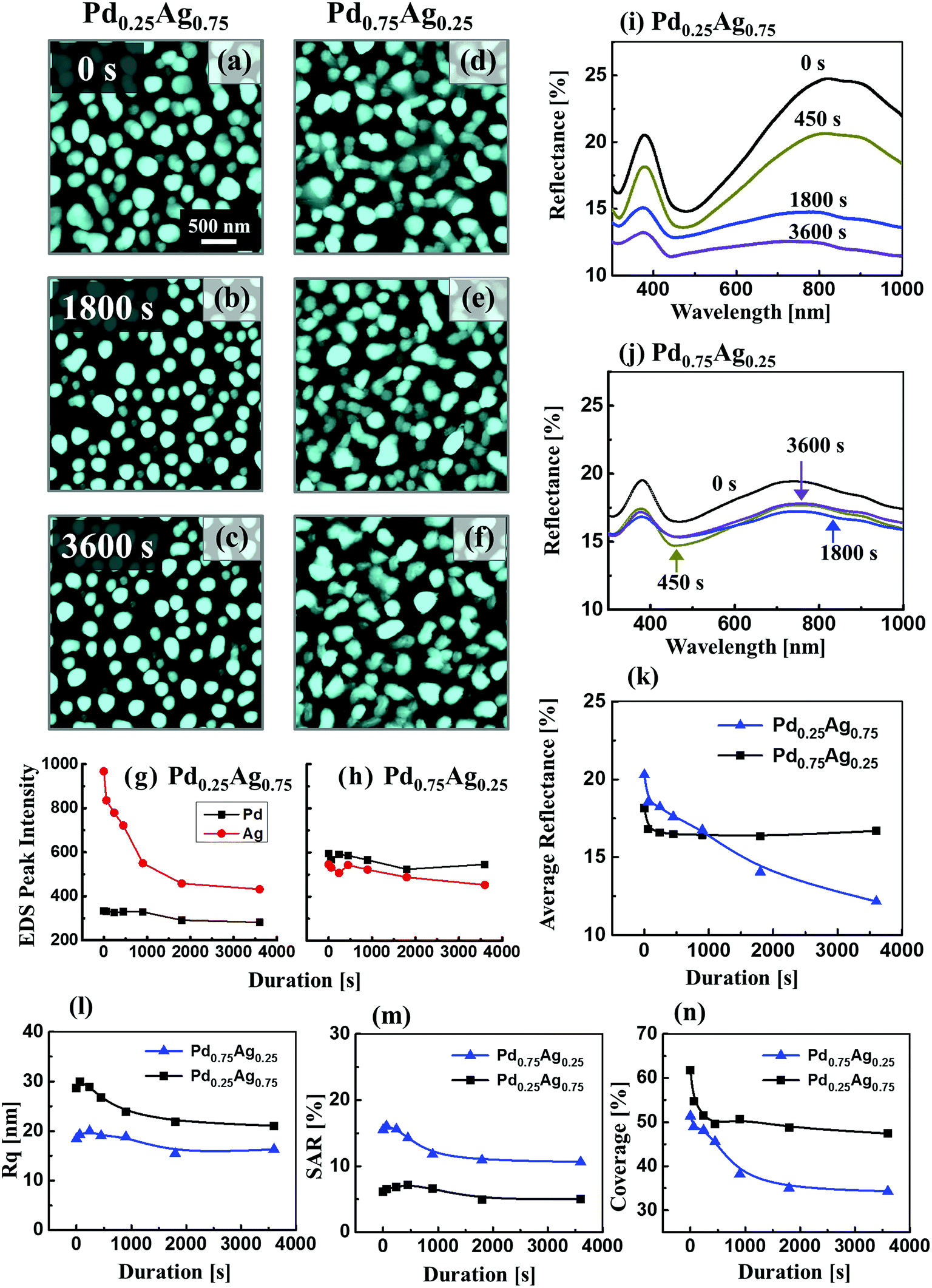
Fig. 6 presents the investigation of annealing duration effect on the evolution of Ag–Pd BMNPs at 650 °C with the distinct bilayer composition (Pd0.25Ag0.75 and Pd0.75Ag0.25) of 10 nm total thickness. The large-scale AFM images, line profiles and specific values of Rq and SAR are supplied in the ESI Fig. S11–14 and Table S7.† In this set, thinner (10 nm) bilayers were adpated to study the dewetting enhancement along with the elongated annealing duration. Generally, well-structured Ag–Pd BMNPs were fabricated in both bilayer compositions due to the enhanced diffusion and inter-mixing of atoms for thinner bilayer films while a sharp distinction was witnessed between two bilayer compositions. For instance, the Pd0.25Ag0.75 demonstrated the formation of isolated-spherical NPs at 0 s. Then, they were gradually becoming more regular and isolated along with the annealing duration. However, irregular-connected Ag–Pd BMNPs were formed with the increased Pd component as shown in second column due to the low diffusivity of Pd atoms. As the overall diffusivity of bilayers was suppressed with the increased Pd content, the irregular NPs were resulted with the increased spacing up to 3600 s. In both cases, when the annealing duration was increased, the overall dewetting was progressively improved, such that Ag–Pd NPs became more regular shape and the inter-spacing was gradually increased. This can be attributed to the enhanced diffusion and agglomeration of adatoms with longer diffusion time, partial sublimation of Ag and shape transformation to gain the equilibrium configuration. Furthermore, the Pd0.25Ag0.75 showed gradual decrease in overall dimension of BMNPs with the annealing duration, which can be due to the Ag sublimation as discussed.39 As evidenced by the EDS summary plots in Fig. 6(g), there observed an exponential drop in Ag count indicating the sublimation loss. However, the Ag sublimation was not too obvious for the Pd0.75Ag0.25 composition due to the initially lower content as shown in Fig. 6(h). In terms of Rq, SAR and coverage as shown in the Fig. 6(l) and (m), the Pd0.25Ag0.75 set showed relatively higher Rq values, suggesting the enhanced vertical growth of NPs due to the sufficient surface diffusion with the higher Ag component. Along with the annealing duration, the Rq was gradually reduced due to the dimensional decrease of alloy NPs by the Ag sublimation. Similar evolution trend of SAR was observed as shown in Fig. 6(m). In terms of the surface coverage, it was generally decreased along with the annealing duration due to the formation of isolated NPs with size devolution. More specifically, the Pd0.75Ag0.25 set exhibited higher coverage as compared to the Pd0.25Ag0.75. Fig. 6(i)–(k) show the reflectance spectra of the Ag–Pd BMNPs, fabricated with the control of annealing duration. In response to the morphology change, the reflectance spectra were clearly modulated for both bilayer compositions as displayed in Fig. 6(i) and (j). For the Pd0.25Ag0.75 composition, a sharp UV peak, dip in visible region and broader NIR peak were witnessed corresponding to the surface plasmon resonance of alloy NPs as discussed.42 The UV peak was consistently found at ∼380 nm for all samples whereas the NIR peak was firstly observed ∼850 nm at 0 s and gradually became weaker. At that same time, the absorption band was slightly blue-shifted to ∼750 nm for longer annealing duration due to the shift of resonance wavelength based on the size reduction of alloy NPs.49,50 Also, the significant decrease in the peak intensity and broadening was observed, which can be related to the decreased Ag composition along with the sublimation. Meanwhile, for Pd0.75Ag0.25, while the UV peak was observed at ∼380 nm, the NIR peak was slightly below 800 nm likely due to lager Pd component in the NPs. On the other hand, the peak intensity was much weaker as compared to previous sets as the NPs consist of lower Ag. In terms of average reflectance, it was generally decreased along with the annealing duration and showed a similar trend with the surface coverage as shown in Fig. 6(k) and (n). More specifically, the average reflectance was decreased sharply in case of Pd0.25Ag0.75 whereas the Pd0.75Ag0.25 set showed minor reduction depending upon the morphology evolution and average coverage.
 |
| | Fig. 6 Evolution of Ag–Pd bimetallic nanostructures by the variation of annealing durations between 0 and 3600 s at 650 °C with the deposition thickness of 10 nm and distinct bilayer composition as labelled. (a)–(f) AFM top-views of 3 × 3 μm2. (g) and (h) Summary of EDS intensities of Ag Lα1 and Pd Lα1 with respect to the annealing durations. (i) and (j) Reflectance spectra of Ag–Pd nanostructures. (k) Summary plot of average reflectance. (l)–(n) Summary plot of Rq, SAR and coverage plots with respect to the annealing duration. | |
Conclusions
In summary, the dewetting of Ag/Pd bilayers on sapphire (0001) was demonstrated to fabricate various structures of Ag–Pd BMNPs by controlling the annealing temperature, duration, bilayers thickness, composition and deposition sequence. Based on the control of growth conditions, the dewetting of bilayers was readily differed resulting in the formation of diverse Ag–Pd BMNPs such as; irregular-connected, elongated-spherical and spherical configuration by means of diffusion and inter-diffusion of Ag and Pd atoms. At relatively low temperature (<600 °C), the thick Pd top-layer was found to hinder the dewetting process however, the surface morphology was drastically transformed from layers to isolated NPs at 700 °C. On the other hand, the Ag sublimation at high temperature caused the overall size reduction of BMNPs. From the time evolution of Ag–Pd bimetallic NPs, further improvement in the structural configurations were gradually witnessed due to the enhanced diffusion of atoms. By the control of deposition thickness, the dimension, density and spacing of BMNPs were modulated over wide range based on equilibrium configurational and coalescence growth mechanism. The influence of bilayer composition demonstrate drastic change in the dewetting process, such as high Pd composition exhibited extra thermal stability against dewetting. A strong dependency of the reflectance spectra on the surface morphology of Ag–Pd BMNPs was probed, i.e. a UV peak didn't respond the morphology change but the NIR peaks showed gradual blue-shift with size reduction. In addition, the peak intensity and absorption band were significantly affected by the Ag concentration on NPs. This work can potentially be used as a simple approach to fabricate the Ag–Pd bimetallic NPs for plasmonic and catalytic applications.
Conflicts of interest
The authors declare that they have no competing interests.
Acknowledgements
Financial support from the National Research Foundation of Korea (no. 2011-0030079 and 2016R1A1A1A05005009), and in part by the research grant of Kwangwoon University in 2017 is gratefully acknowledged.
References
- M. Höltig, et al., Highly efficient fuel cell electrodes from few-layer graphene sheets and electrochemically deposited Palladium nanoparticles, J. Phys. Chem. C, 2016, 120(14), 7476–7481 Search PubMed.
- J.-r. Choi, et al., Current achievements of nanoparticle applications in developing optical sensing and imaging techniques, Nano Convergence, 2016, 3(1), 30 CrossRef PubMed.
- M. Höltig, et al., Highly efficient fuel cell electrodes from few-layer graphene sheets and electrochemically deposited Palladium nanoparticles, J. Phys. Chem. C, 2016, 120(14), 7476–7481 Search PubMed.
- H. Miura, et al., Supported Palladium–Gold Alloy Catalysts for Efficient and Selective Hydrosilylation under Mild Conditions with Isolated Single Palladium Atoms in Alloy Nanoparticles as the Main Active Site, ACS Catal., 2017, 7(3), 1543–1553 CrossRef CAS.
- C. Chang, et al., Efficient Solar-Thermal Energy Harvest Driven by Interfacial Plasmonic Heating-Assisted Evaporation, ACS Appl. Mater. Interfaces, 2016, 8(35), 23412–23418 CAS.
- T. Jiang, et al., old and gold–palladium alloy nanoparticles on heterostructured TiO2 nanobelts as plasmonic photocatalysts for benzyl alcohol oxidation, Nanoscale, 2015, 7(1), 209–217 RSC.
- M. M. Claudia and R. Spolenak, Dewetting of Au and AuPt alloy films: a dewetting zone model, J. Appl. Phys., 2013, 113(9), 094301 CrossRef.
- W. Li and F. Chen, Alloying effect on performances of bimetallic Ag–Au cluster sensitized solar cells, J. Alloys Compd., 2015, 632, 845–848 CrossRef CAS.
- M. Legawiec-Jarzyna, A. Srebowata and Z. Karpinski, Hydrodechlorination of dichlorodifluoromethane (CFC-12) over Pd/Al2O3 and Pd-Au/Al2O3 catalysts, React. Kinet. Catal. Lett., 2003, 79(1), 157–163 CrossRef CAS.
- A. M. Venezia, V. La Parola, B. Pawelec and J. L. G. Fierro, Hydrogenation of aromatics over Au-Pd/SiO2-Al2O3 catalysts; support acidity effect, Appl. Catal., A, 2004, 264(1), 43–51 CrossRef CAS.
- M.-K. Kwon, J.-Y. Kim, B.-H. Kim, I.-K. Park, C.-Y. Cho, C. C. Byeon and S.-J. Park, Surface-plasmon-enhanced light-emitting diodes, Adv. Mater., 2008, 20(7), 1253–1257 CrossRef CAS.
- K. Jia, et al., Strong improvements of localized surface plasmon resonance sensitivity by using Au/Ag bimetallic nanostructures modified with polydopamine films, ACS Appl. Mater. Interfaces, 2013, 6(1), 219–227 Search PubMed.
- M. Tang, et al., Broad-band plasmonic Cu-Au bimetallic nanoparticles for organic bulk heterojunction solar cells, Org. Electron., 2016, 38, 213–221 CrossRef CAS.
- H. F. Zarick, et al., Improving Light Harvesting in Dye-Sensitized Solar Cells Using Hybrid Bimetallic Nanostructures, ACS Photonics, 2016, 3(3), 385–394 CrossRef CAS.
- K. Sugawara, Y. Minamide, M. Kawamura, Y. Abe and K. Sasaki, Agglomeration behavior of Ag films suppressed by alloying with some elements, Vacuum, 2008, 83(3), 610–613 CrossRef CAS.
- A. Panáček, L. Kvítek, R. Prucek, M. Kolář, R. Večeřová, N. Pizúrová, V. K. Sharma, T. Nevěčná and R. Zbořil, Silver colloid nanoparticles: synthesis, characterization, and their antibacterial activity, J. Phys. Chem. B, 2006, 110(33), 16248–16253 CrossRef PubMed.
- S. Kunwar, M. Sui, Q. Zhang, P. Pandey, M.-Y. Li and J. Lee, Ag nanostructures on GaN (0001): morphology evolution controlled by the solid state dewetting of thin films and corresponding optical properties, Cryst. Growth Des., 2016, 16(12), 6974–6983 CAS.
- E. Jiran and C. V. Thompson, Capillary instabilities in thin, continuous films, Thin Solid Films, 1992, 208(1), 23–28 CrossRef CAS.
- A. B. Tesler, B. M. Maoz, Y. Feldman, A. Vaskevich and I. Rubinstein, Solid-state thermal dewetting of just-percolated gold films evaporated on glass: development of the morphology and optical properties, J. Phys. Chem. C, 2013, 117(21), 11337–11346 CAS.
- F. Ruffino and M. G. Grimaldi, Template-confined
dewetting of Au and Ag nanoscale films on mica substrate, Appl. Surf. Sci., 2013, 270, 697–706 CrossRef CAS.
- E. J. Luber, B. C. Olsen, C. Ophus and D. Mitlin, Solid-state dewetting mechanisms of ultrathin Ni films revealed by combining in situ time resolved differential reflectometry monitoring and atomic force microscopy, Phys. Rev. B: Condens. Matter Mater. Phys., 2010, 82(8), 085407 CrossRef.
- E. J. Luber, B. C. Olsen, C. Ophus and D. Mitlin, Solid-state dewetting mechanisms of ultrathin Ni films revealed by combining in situ time resolved differential reflectometry monitoring and atomic force microscopy, Phys. Rev. B: Condens. Matter Mater. Phys., 2010, 82(8), 085407 CrossRef.
- K. K. Nanda, S. N. Sahu and S. N. Behera, Liquid-drop model for the size-dependent melting of low-dimensional systems, Phys. Rev. A: At., Mol., Opt. Phys., 2002, 66(1), 013208 CrossRef.
- I. Beszeda, E. G. Gontier-Moya and A. W. Imre, Surface Ostwald-ripening and evaporation of gold beaded films on sapphire, Appl. Phys. A: Mater. Sci. Process., 2005, 81(4), 673–677 CrossRef CAS.
- C. V. Thompson, Solid-state dewetting of thin films, Annu. Rev. Mater. Res., 2012, 42, 399–434 CrossRef CAS.
- J.-Y. Kwon, T.-S. Yoon, K.-B. Kim and S.-H. Min, Comparison of the agglomeration behavior of Au and Cu films sputter deposited on silicon dioxide, J. Appl. Phys., 2003, 93(6), 3270–3278 CrossRef CAS.
- P. Pandey, M. Sui, M.-Y. Li, Q. Zhang, E.-S. Kim and J. Lee, Systematic study on the self-assembled hexagonal Au voids, nano-clusters and nanoparticles on GaN (0001), PLoS One, 2015, 10(8), e0134637 Search PubMed.
- D. T. Danielson, D. K. Sparacin, J. Michel and L. C. Kimerling, Surface-energy-driven dewetting theory of silicon-on-insulator agglomeration, J. Appl. Phys., 2006, 100(8), 083507 CrossRef.
- L. Rayleigh, On the instability of jets, Proc. Lond. Math. Soc., 1878, 1(1), 4–13 CrossRef.
- J. A. Venables, G. D. T. Spiller and M. Hanbucken, Nucleation and growth of thin films, Rep. Prog. Phys., 1984, 47(4), 399 CrossRef.
- M. Sui, P. Pandey, M.-Y. Li, Q. Zhang, S. Kunwar and J. Lee, Tuning the configuration of Au nanostructures: from vermiform-like, rod-like, triangular, hexagonal, to polyhedral nanostructures on c-plane GaN, J. Mater. Sci., 2017, 52(1), 391–407 CrossRef CAS.
- P. M. Hall, J. M. Morabito and J. M. Poate, Diffusion mechanisms in the Pd/Au thin film system and the correlation of resistivity changes with Auger electron spectroscopy and Rutherford backscattering profiles, Thin Solid Films, 1976, 33(1), 107–134 CrossRef CAS.
- M. A. Noah, D. Flötotto, Z. Wang and E. J. Mittemeijer, Interdiffusion and stress development in single-crystalline Pd/Ag bilayers, J. Appl. Phys., 2016, 119(14), 145308 CrossRef.
- S. Arai and J. Fujii, Electroless deposition of silver on multiwalled carbon nanotubes using iodide bath, J. Electrochem. Soc., 2011, 158(8), D506–D510 CrossRef CAS.
- F. Ruffino, V. Torrisi, G. Marletta and M. G. Grimaldi, Growth morphology of nanoscale sputter-deposited Au films on amorphous soft polymeric substrates, Appl. Phys. A: Mater. Sci. Process., 2011, 103(4), 939–949 CrossRef CAS.
- C. T. Campbell, Ultrathin metal films and particles on oxide surfaces: structural, electronic and chemisorptive properties, Surf. Sci. Rep., 1997, 27(1–3), 1–11 CrossRef CAS.
- L. Zhang, F. Cosandey, R. Persaud and T. E. Madey, Initial growth and morphology of thin Au films on TiO2(110), Surf. Sci., 1999, 439(1), 73–85 CrossRef CAS.
- M. Zinke-Allmang, L. C. Feldman and M. H. Grabow, Clustering on surfaces, Surf. Sci. Rep., 1992, 16(8), 377–463 CrossRef CAS.
- M. Sui, P. Pandey, S. Kunwar, M. Y. Li, Q. Zhang and J. Lee, Evolution of self-assembled Ag nanostructures
on c-plane sapphire by the systematic control of annealing temperature, Superlattices Microstruct., 2016, 100, 1128–1142 CrossRef CAS.
- M. Sui, Q. Zhang, S. Kunwar, P. Pandey, M. Y. Li and J. Lee, Study on the dimensional, configurational and optical evolution of palladium nanostructures on c-plane sapphire by the control of annealing temperature and duration, Appl. Surf. Sci., 2017, 416, 1–3 CrossRef CAS.
- P. Pandey, S. Kunwar, M. Sui, M.-Y. Li, Q. Zhang and J. Lee, Fabrication of Ag nanostructures by the systematic control of annealing temperature and duration on GaN (0001) via the solid state dewetting, Phys. Status Solidi A, 2017, 214(3), 1600702 CrossRef.
- E. Thouti, N. Chander, V. Dutta and V. K. Komarala, Optical properties of Ag nanoparticle layers deposited on silicon substrates, J. Opt., 2013, 15(3), 035005 CrossRef.
- S. Kunwar, M. Sui, Q. Zhang, P. Pandey, M. Y. Li and J. Lee, Various silver nanostructures on sapphire using plasmon self-assembly and dewetting of thin films, Nano-Micro Lett., 2017, 9(2), 17 CrossRef.
- S. Kunwar, M. Sui, P. Pandey, Q. Zhang, M. Y. Li, H. Bhandari and J. Lee, Determination of growth regimes of Pd nanostructures on c-plane sapphire by the control of deposition amount at different annealing temperatures, Phys. Chem. Chem. Phys., 2017, 19(23), 15084–15097 RSC.
- H. Proehl, R. Nitsche, T. Dienel, K. Leo and T. Fritz, In situ differential reflectance spectroscopy of thin crystalline films of PTCDA on different substrates, Phys. Rev. B: Condens. Matter Mater. Phys., 2005, 71(16), 165207 CrossRef.
- K. H. Hansen, T. Worren, S. Stempel, E. Lægsgaard, M. Bäumer, H.-J. Freund, F. Besenbacher and I. Stensgaard, Palladium nanocrystals on Al2O3: structure and adhesion energy, Phys. Rev. Lett., 1999, 83(20), 4120 CrossRef CAS.
- J. Feng, W. Zhang and W. Jiang, Ab initio study of Ag/Al2O3 and Au/Al2O3 interfaces, Phys. Rev. B: Condens. Matter Mater. Phys., 2005, 72(11), 115423 CrossRef.
- E. J. Guidelli, O. Baffa and D. R. Clarke, Enhanced UV emission from silver/ZnO and gold/ZnO core-shell nanoparticles: photoluminescence, radioluminescence, and optically stimulated luminescence, Sci. Rep., 2015, 5, 14004 CrossRef CAS PubMed.
- S. Agnihotri, S. Mukherji and S. Mukherji, Size-controlled silver nanoparticles synthesized over the range 5–100 nm using the same protocol and their antibacterial efficacy, RSC Adv., 2014, 4(8), 3974–3983 RSC.
- U. Guler and R. Turan, Effect of particle properties and light polarization on the plasmonic resonances in metallic nanoparticles, Opt. Express, 2010, 18(16), 17322–17338 CrossRef CAS PubMed.
Footnote |
| † Electronic supplementary information (ESI) available. See DOI: 10.1039/c7ra11058h |
|
| This journal is © The Royal Society of Chemistry 2017 |
Click here to see how this site uses Cookies. View our privacy policy here. 
 Open Access Article
 This Open Access Article is licensed under a
  *ab
*ab