
 Open Access Article
 This Open Access Article is licensed under a
 Creative Commons Attribution 3.0 Unported Licence
Peculiar electronic, strong in-plane and out-of-plane second harmonic generation and piezoelectric properties of atom-thick α-M2X3 (M = Ga, In; X = S, Se): role of spontaneous electric dipole orientations†
Lei Hu * and
Xuri Huang*
* and
Xuri Huang*
Institute of Theoretical Chemistry, Jilin University, Changchun 130000, People's Republic of China. E-mail: 598450225@qq.com; Xurihuang12@gmail.com
First published on 4th December 2017
Abstract
Second harmonic generation (SHG) and piezoelectric properties of two-dimensional (2D) materials are sparking great interest. However, out-of-plane SHG in 2D materials has been rarely reported; the theoretical out-of-plane piezoelectric response in atom-thick 2D materials is very limited at the present stage. α-M2X3 monolayers exhibit out-of-plane spontaneous polarizations, promising out-of-plane SHG and piezoelectricity. Here, we perform first-principles calculations of the electronic, SHG and piezoelectric properties of single- and few-layer α-M2X3. Results indicate the bandgaps of α-M2X3 monolayers are in the visible range, and become much narrower as the layer number goes up. Furthermore, the narrower bandgaps are broadened by more than 1.00 eV by switching the electric dipole orientation in few-layer α-M2X3. α-M2X3 monolayers exhibit superior in-plane and out-of-plane SHG properties; in particular, their out-of-plane SHG coefficients are comparable with those of GaAs crystals. Furthermore, the out-of-plane SHG coefficients can be effectively tuned by switching the electric dipole orientation in α-M2X3 few-layers. α-M2X3 monolayers exhibit superior in-plane and considerable out-of-plane piezoelectricity, and the latter is significantly enhanced in bilayer α-M2X3 because of the built-in electric field originating from the parallel electric dipoles. Our work will stimulate research on the ultrathin 2D photo detection, SHG and piezoelectric devices.
1. Introduction
Second harmonic generation (SHG) and piezoelectric properties caused by noncentrosymmetry in two-dimensional (2D) atom-thick materials are sparking great interest. For instance, 2D MoS2,1,2 GaSe,3,4 SiC,5 BN6 and GeC7 nanosheets display fascinating prospects in ultrathin SHG devices. However, these 2D materials only exhibit in-plane SHG properties as they embody out-of-plane centrosymmetric characters, i.e. out-of-plane SHG has not been discovered in these 2D materials. On the other hand, monolayer BN,8 MoS2,9 GaSe,10 GaSSe,11 buckled hexagonal compounds12 and doped graphene,13 have a wide range of applications including in mechanical stress sensors, actuators and energy harvesting devices14 since they are piezoelectric. Even though a recent calculation has found strong out-of-plane piezoelectricity in multilayer MoSTe15 and a recent experiment has shown that out-of-plane piezoelectricity occurs in multilayer (10 nm-thick) α-In2Se3 flakes,16 the obtained out-of-plane piezoelectricity in atom-thick 2D materials such as monolayers11–13 and bilayers is very limited. This makes it impossible to fabricate effective ultrathin 2D piezoelectric devices allowing out-of-plane mechanical–electrical energy conversions.On the other hand, 2D nanosheets exfoliated from α- and β-In2Se3 bulk crystals are attracting great attention in the aspects of the thermal conductivity, phase transformation,17,18 photo-responsibility,19,20 sensitivity,21 dielectric22 and optical properties.23 The electric field perpendicular to α- and β-In2Se3 monolayers induce a semiconductor to metal transition.24 Remarkably, the class of α-M2X3 ferroelectric monolayers exhibit in-plane and out-of-plane reversible spontaneous polarizations,25 promising in-plane and out-of-plane SHG and piezoelectric responses. Indeed, out-of-plane SHG has been recently discovered in monolayer α-In2Se3; however the features and magnitude of the SHG coefficients are still unknown.16 Moreover, monolayer multiferroics exhibit very small out-of-plane SHG coefficients χ(2)zzy and χ(2)zyz.26 This simulates us to explore the SHG and piezoelectricity of α-M2X3 monolayers using first-principles calculations, expecting to find strong out-of-plane SHG and piezoelectricity.
Experiments indicate that the physical properties of In2Se3 multilayer nanosheets, such as optical bandgap23 and thermal conductivity,17 show a strong layer-dependent behavior. These remind us to study the correlation between the layer thickness and the electronic, piezoelectric and SHG properties of atomic-thick M2X3 nanosheets. It should be noted that the nanosheet in our theoretical calculations is much thinner than that in previous experiments.17,23 Moreover, the van der Waals heterostructure of α-In2Se3/WSe2 shows a significant bandgap reduction when switching the electric dipole orientation of the In2Se3 layer. In essence, switching the electric orientation is changing stacking sequences. It has been shown SHG of few-layer GaSe nanosheets27 and piezoelectricity of multilayer MoSTe15 can be effectively tuned by using various stacking sequences. Therefore, it is meaningful to explore how the electric dipole orientation affects the electronic, piezoelectric and SHG properties of few-layer M2X3.
2. Calculation models and details
Single- and few-layer β-M2X3 nanosheets are centrosymmetric, their piezoelectricity and SHG vanish. We thereby study the electronic, piezoelectric and SHG properties of monolayer α-M2X3 (M = Ga, In; X = S, Se), and their top and side views are displayed in Fig. 1. To study the layer-dependent behavior, the bilayer and trilayer exfoliated from α-Ga2S3 and α-In2Se3 bulk crystals are considered, which are respectively named as AA and AAA stacking. Furthermore, to investigate the effect of the electric dipole orientation, bilayer AB is achieved by switching the electric dipole orientation of the bottom layer in AA, while trilayer ABA is attained by switching the electric dipole orientation of the middle layer in AAA.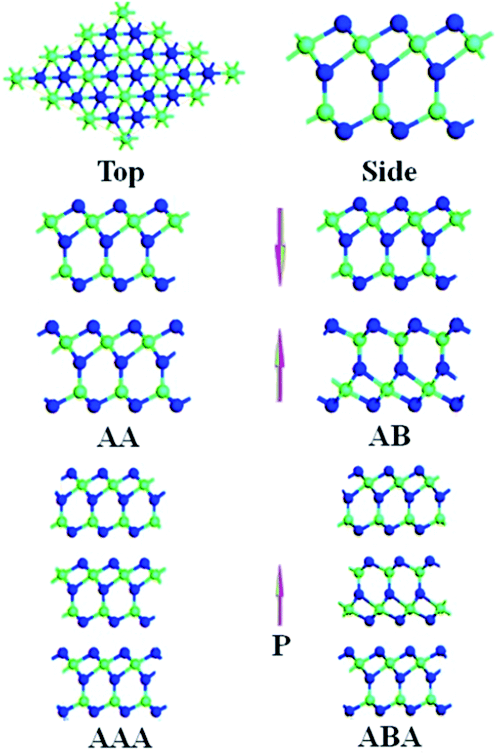 | ||
| Fig. 1 Schematics of top and side views of monolayer α-M2X3. The green atoms denote M (M = Ga, In) atoms, while the blue atoms denote X (X = S, Se) atoms. This figure represents bilayer AB is achieved by switching the electric dipole orientation of the bottom α-M2X3 layer in bilayer AA, and trilayer ABA is obtained by switching the electric dipole orientation of the middle α-M2X3 layer in trilayer AAA. | ||
All calculations are on the basis of the density functional theory (DFT) using the projector-augmented wave (PAW)28 method as implemented in the Vienna Ab initio Simulation Package (VASP).29–32 The generalized gradient approximation (GGA) parameterized by Perdew, Burke, and Ernzerhof (PBE)33 with van der Waals (vdW) correction proposed by Crimme (DFT-D2)34 is employed. The single electron wave functions are expanded with a large wave cutoff energy of 500 eV. To minimize the periodic interaction along the z axis, the vacuum spacing between adjacent nanosheets is set to be at least 20 Å. A gamma-centered k-point grid of 11 × 11 × 1 is used to optimize geometry structures, and the convergence criteria for electronic and ionic relaxations are respectively set as 10−7 and 10−3 eV Å−1. A k-point grid of 31 × 31 × 1 is used to calculate piezoelectric coefficients of monolayers and few-layers. The more dense k-point grid of 60 × 60 × 1 is used to obtain SHG coefficients of monolayers, while the k-point of 45 × 45 × 1 is applied for few-layers.
3. Results and discussions
3.1. Structural properties
As shown in Fig. 1, α-M2X3 monolayers are five atoms thick, with atoms arranged in the sequence of X–M–X–M–X in the direction perpendicular to the layers. Table 1 summarizes the calculated in-plane constant a and effective thickness h of α-M2X3 monolayers. As the α-M2X3 bulk crystal contains three basic layers, the theoretical h of α-M2X3 monolayers is simply taken as 1/3 of the lattice constant c of optimized bulk crystals. The calculated h are larger than that of monolayer MX2 (M = Mo, W; X = S, Se)35 and GaX (X = S, Se, Te),27 indicating a stronger SHG intensity in α-M2X3 monolayers than that in MoX2 and GaX monolayers as the SHG intensity shows a quadratic dependence on the thickness, according to the dipole theory.4 It is very convenient to identify layer numbers of α-M2X3 nanosheets using the effective thickness value in further experiments, which will accelerate explorations of their properties.| a | h | EPBEg | EHSE06g | EHSE06min | χ(2)xxy(0) | χ(2)zxx(0) | χ(2)zzz(0) | ||
|---|---|---|---|---|---|---|---|---|---|
| α-Ga2S3 | ML | 3.59 | 8.94 | 1.79(I) | 2.95(I) | 3.25(G) | 25.4 | 23.8 | 162.6 |
| AA | 3.59 | 17.88 | 0.65(I) | 1.80(I) | 2.05(G) | 23.0 | 27.4 | 184.2 | |
| AB | 3.59 | 17.88 | 1.64(I) | 2.80(I) | 3.04(G) | 25.0 | −0.3 | 0.8 | |
| ABA | 3.59 | 26.82 | 1.52(I) | 2.64(I) | 2.81(G) | 24.2 | 6.4 | 47.6 | |
| α-Ga2Se3 | ML | 3.77 | 9.40 | 1.06(I) | 2.04(I) | 2.30(G) | 34.6 | 26.2 | 208.0 |
| α-In2S3 | ML | 3.83 | 9.18 | 1.29(I) | 2.30(I) | 2.36(G) | 30.6 | 36.6 | 207.6 |
| α-In2Se3 | ML | 3.99 | 9.68 | 0.88(I) | 1.80(I) | 1.83(G) | 42.2 | 41.8 | 252.6 |
| AB | 3.99 | 19.36 | 0.57(I) | 1.45(I) | 1.46(G) | 44.0 | −1.80 | −0.02 | |
| ABA | 4.00 | 29.04 | 0.45(I) | 1.25(I) | 1.26(G) | 48.2 | 8.2 | 61.4 |
Similar to previous calculations,36 the formation energies of single- and few-layer α-M2X3 nanosheets are defined as Ef = E/N − Eref/Nref, where E and Eref are respectively the energies of nanosheets and corresponding bulk crystals. N and Nref are the numbers of atoms in the respective unit cells. The calculated formation energies of monolayer α-M2X3, few-layer α-Ga2S3 and α-In2Se3 are shown in Fig. 2. The formation energies of α-M2X3 monolayers are comparable or even smaller than that of monolayer MoS2. The formation energies of monolayer, bilayer AA, and trilayer AAA α-Ga2S3 (α-In2Se3) decrease as their layer numbers increase, suggesting it is more likely to successfully obtain α-Ga2S3 (α-In2Se3) nanosheets with larger layer numbers. Indeed, trilayer AAA α-In2Se3, i.e. 3.1 nm-thick α-In2Se3 nanosheets have been synthesized using mechanical exfoliation.23 Moreover, the formation energy of α-Ga2S3 nanosheets is to some extent smaller than that of corresponding α-In2Se3 nanosheets, indicating it is more likely to obtain α-Ga2S3 nanosheets. Furthermore, the difference of the formation energy can be negligible for AA (AAA) and AB (ABA), ensuring the feasibility to achieve AB (ABA) by switching the electric dipole orientation in AA (AAA) from the standpoint of energetics.
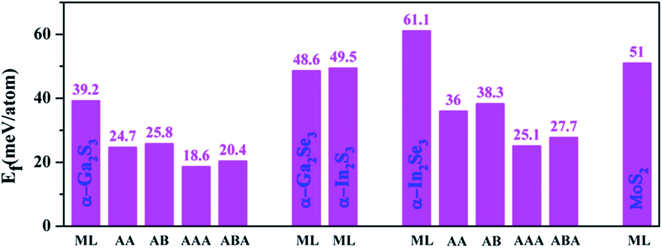 | ||
| Fig. 2 Calculated formation energies of monolayer α-M2X3, few-layer α-Ga2S3 and α-In2Se3. The formation energy of the synthesized MoS2 monolayer is shown for comparison. | ||
3.2. Electronic properties
In contrast to the previous bandgap calculation using the HSE06 functional with 25% exact exchange,25 we calculated the band structure of single-layer α-M2X3 using 30% EE, cf. ESI (SI-1†). The calculated band structures are displayed in Fig. 3. α-M2X3 monolayers are indirect bandgap semiconductors with their valence band maximum (VBM) located between the M (0.0, 0.5, 0.0) and gamma (0.0, 0.0, 0.0) points. The conduction band minimum (CBM) is located at the M point for monolayer α-Ga2S3 and α-Ga2Se3, while for single-layer α-In2S3 and α-In2Se3 it is located at the gamma point. The top valence band of α-M2X3 monolayers is relatively flat, resulting in a high density of electronic states in the top valence band region as shown in Fig. 3(e), which is the origin of large SHG coefficients.7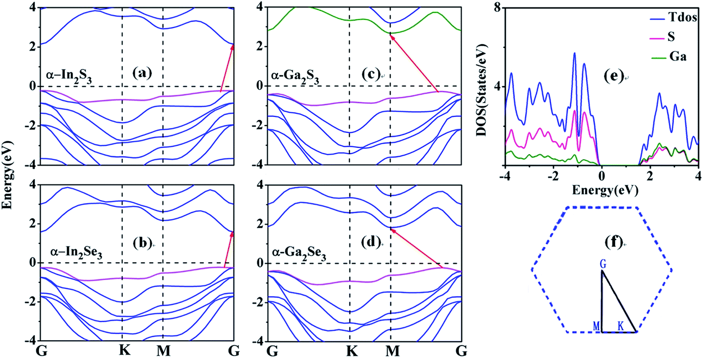 | ||
| Fig. 3 Calculated band structure of (a) α-In2S3, (b) α-In2Se3, (c) α-Ga2S3 and (d) α-Ga2Se3 using HSE06 incorporating 30% EE. (e) Total and partial density of states of monolayer α-Ga2S3 calculated using PBE. (f) The high symmetry k-point path in the Brillouin Zone is chosen as: gamma (0, 0, 0) → k (−1/3, 2/3, 0) → M (0, 1/2, 0) → gamma (0, 0, 0), and gamma is abbreviated as G. | ||
Table 1 summarizes the PBE and HSE06 bandgaps of α-M2X3 monolayers. The PBE bandgap of 0.88 eV for monolayer α-In2Se3 gets very close to the calculated bandgap of 0.82 eV using PBE + SOC,24 suggesting spin-orbital coupling (SOC) does not significantly modify the electronic property. The HSE06 bandgap of 1.80 eV for single-layer α-In2Se3 gets close to the calculated bandgap of 1.92 eV using the GW approximation,24 but slightly larger than the bandgap of 1.45 eV calculated using HSE06 with 25% exact exchange.25 The energy gaps of each monolayer at the gamma point are close to their respective indirect bandgaps, which is more evident for α-In2S3 and α-In2Se3 monolayers. It is expected the interband optical transition at the gamma point improves optical responses of α-M2X3 monolayers because no phonons are required for this optical transition to proceed. Additionally, the HSE06 bandgaps of α-M2X3 monolayers are large enough to avoid current leakages, and thereby they are promising in piezoelectric devices.
Fig. 4 displays the band structures of bilayer AA and AB, and trilayer ABA α-Ga2S3 calculated using HSE06. If there were no interlayer interaction, the band structure of bilayer AA α-Ga2S3 should be identical to that of monolayer α-Ga2S3. Nevertheless, the bands from different α-Ga2S3 layers in AA are pronouncedly splitted. Comparisons of Fig. 3(c) and 4(c) show the bottom valence bands from various α-Ga2S3 layers in AA are splitted by as large as 1.31 eV. Resultantly, the bandgap of AA significantly gets reduced by 1.15 eV in comparison with that of monolayer α-Ga2S3 as Table 1 shows, and that of trilayer AAA α-Ga2S3 further decreases as shown in Fig. 4(a). In brief, we find the bandgap of few-layer α-Ga2S3 nanosheets becomes much narrower as their layer number increases. This bandgap reduction is also pronounced for few-layer α-In2Se3 nanosheets. Fig. 4(a) indicates the bandgap of trilayer AAA α-In2Se3 nearly vanishes. Similarly, optical absorption spectra show the bandgap decreases from 2.80 eV to 1.45 eV as the layer thickness increases from 3.1 nm to 20.1 nm.23 Considering the effective thickness of monolayer α-In2Se3 is ∼1 nm, the optical bandgap of 1.45 eV for α-In2Se3 nanosheets with ∼20 layers gets close to our theoretical value of 1.48 eV for α-In2Se3 bulk crystals. Nevertheless, the experimental bandgap of 2.8 eV for 3.1 nm-thick (trilayer) α-In2Se3 nanosheets significantly varies from the zero bandgap of trilayer AAA α-In2Se3. Moreover, PBE calculations also find the bandgap of bilayer AA and trilayer AAA α-In2Se3 is closed.25 It seems further bandgap measurements of few-layer α-In2Se3 are emergently needed to interpret the huge divergence between experimental and theoretical bandgaps. On the other hand, we note the band splitting in non-ferroelectric MoS2 nanosheets is not so pronounced.35 Single-layer MoS2 embodies out-of-plane centrosymmetric characters and in-plane non-centrosymmetric characters. Therefore, the pronounced band splitting in few-layer α-Ga2S3 (α-In2Se3) nanosheets is caused by the built-in electric field originated from the parallel out-of-plane electric polarizations (dipoles) of α-Ga2S3 (α-In2Se3) layers (cf. ESI-3†). This is further affirmed by semiconducting α-In2Se3 monolayers becoming metallic when an electric filed perpendicular is applied.24
 | ||
| Fig. 4 (a) Bandgap variation of monolayer (ML), bilayer AA and AB, trilayer AAA and ABA α-Ga2S3 (α-In2Se3) nanosheets. Calculated Band structure of bilayer (c) AA and (d) AB, and (b) trilayer ABA α-Ga2S3 calculated using HSE06. Total and partial density of states (DOS) of bilayer (e) AA and (f) AB α-Ga2S3 calculated using PBE. | ||
The band splitting of bilayer AB α-Ga2S3 is not pronounced, and accordingly the bandgap difference between monolayer and bilayer AB α-Ga2S3 is very small. This is because the built-in electric field significantly decreases as the out-of-plane electric polarizations (dipoles) of α-Ga2S3 layers are antiparallelly aligned (cf. ESI-3†). Furthermore, the band splitting in Fig. 4(b) is minor in ABA α-Ga2S3 as expected. The divergence of electronic properties between AA and AB α-Ga2S3 is further emphasized in Fig. 4(e) and (f). The peaks in the conduction band region of bilayer AB α-Ga2S3 look similar to that of monolayer α-Ga2S3. Nevertheless, the peaks in AA α-Ga2S3 are significantly splitted, particularly for the peaks between −3 and −2 eV. Briefly, the bandgap in AA α-Ga2S3 is broadened by 1.00 eV in AB α-Ga2S3, which is very advantageous for applications as photodetectors since one can select the sensing photon energy window by switching electric dipole orientation. Additionally, the zero bandgap in AAA α-In2Se3 is opened in ABA α-In2Se3, indicating the semiconducting nature can be achieved by switching the electric dipole orientation.
3.3. SHG properties
The length-gauge formulism at the independent-particle level derived by Aversa and Sipe37 and rearranged by Rashkeev et al.38 is used to calculate second-harmonic generation (SHG) coefficients (cf. ESI-2†), and its details are displayed in a previous work.39 Similar to previous works,7,27 the energy differences between HSE06 and PBE bandgaps are used for scissors corrections to reduce the errors caused by neglected many-body effects;40–42 the effective unit cell volume is applied to reduce underestimations caused by the large vacuum spacing. For α-M2X3 monolayers and few-layers, the effective volume is obtained by multiplying the area of in-plane unit cell and the effective thickness.Because single- and few-layer α-M2X3 belong to C3v symmetry, they have eleven static SHG coefficients and only three of them are independent dictated by Kleiman's symmetry: χ(2)yyy(0) = −χ(2)yxx(0) = −χ(2)xxy(0) = −χ(2)xyx(0), χ(2)zzz(0) and χ(2)zxx(0) = χ(2)zyy(0) = χ(2)yyz(0) = χ(2)yzy(0) = χ(2)xzx(0) = χ(2)xxz(0). The static χ(2)xxy(0), χ(2)zxx(0) and χ(2)zzz(0) are summarized in Table 1. The static χ(2)xxy(0) describes the in-plane SHG phenomenon, which has been discovered in previous experiments of MoS2,2 GaSe4 and BN43 monolayers. Even though the static χ(2)xxy(0) of α-M2X3 monolayers is much smaller than that of MoS2 (ref. 35) and GaSe27 monolayers, it is still comparable with χ(2)zxy(0) of 28.2 pm V−1 for an archetypical nonlinear optical crystal AgGaS2,44 ensuring α-M2X3 monolayers can be used as in-plane two-dimensional SHG devices. More importantly, α-M2X3 monolayers have additional SHG components χ(2)zzz(0) and χ(2)zxx(0) compared with MoS2 and GaSe monolayers. Especially, the calculated χ(2)zzz(0) of α-M2X3 monolayers are comparable or even larger than the static SHG coefficient of 173.2 pm V−1 for GaAs crystals.45 Therefore, α-M2X3 monolayers are of great importance in ultrathin two-dimensional devices allowing strong out-of-plane SHG occurs.
Fig. 5 represents the calculated real and imaginary parts of SHG coefficients χ(2)zzz(−2ω,ω,ω), χ(2)zxx(−2ω,ω,ω) and χ(2)xxy(−2ω,ω,ω) of α-M2X3 monolayers. The χ(2)zzz(−2ω,ω,ω) and χ(2)xxy(−2ω,ω,ω) components are significant in the entire range of optical energy. The χ(2)zzz(−2ω,ω,ω) component is several times larger than χ(2)xxy(−2ω,ω,ω) and χ(2)zxx(−2ω,ω,ω). For χ(2)zxx(−2ω,ω,ω), the electric field of both incoming and outgoing photons is parallel to the z axis, and thereby the electric depolarization vanishes. To analyze the prominent features in SHG spectra, the absolute values of imaginary part of χ(2)zzz(−2ω,ω,ω) and χ(2)xxy(−2ω,ω,ω) for monolayer α-Ga2S3 are plotted in Fig. 6 and compared with the absorptive part of corresponding dielectric function ε′′. The first prominent peak between 1.7 and 3.8 eV in the χ(2)zzz(−2ω,ω,ω) spectrum is caused by double-photon resonances (cf. Fig. 6(a) and (b)). In contrast, the double-peak structure between 3.8 and 5.6 eV in χ(2)zzz(−2ω,ω,ω) comes from single- and double-photon resonances. These single- and double-photon resonances only involve optical transitions for the electric filed vector ![[E with combining right harpoon above (vector)]](https://www.rsc.org/images/entities/i_char_0045_20d1.gif) parallel to the z axis (‖z). Fig. 6 further suggests the first prominent peak between 2.2 and 3.6 eV in the χ(2)xxy(−2ω,ω,ω) spectrum is caused by double-photon resonances with ‖x (cf. Fig. 6(c) and (d)), while the peak between 3.9 and 5.4 eV in χ(2)xxy(−2ω,ω,ω) comes from both single- and double-photon resonances with ‖x.
parallel to the z axis (‖z). Fig. 6 further suggests the first prominent peak between 2.2 and 3.6 eV in the χ(2)xxy(−2ω,ω,ω) spectrum is caused by double-photon resonances with ‖x (cf. Fig. 6(c) and (d)), while the peak between 3.9 and 5.4 eV in χ(2)xxy(−2ω,ω,ω) comes from both single- and double-photon resonances with ‖x.
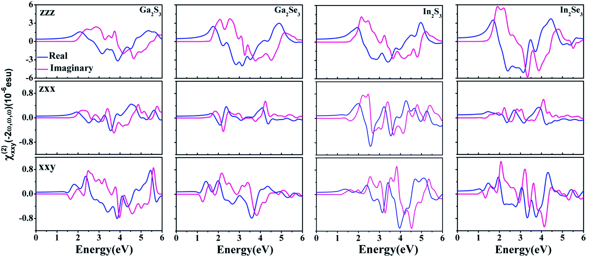 | ||
| Fig. 5 Calculated real and imaginary parts of SHG coefficients χ(2)zzz(−2ω,ω,ω), χ(2)zxx(−2ω,ω,ω) and χ(2)xxy(−2ω,ω,ω) of monolayer α-M2X3. | ||
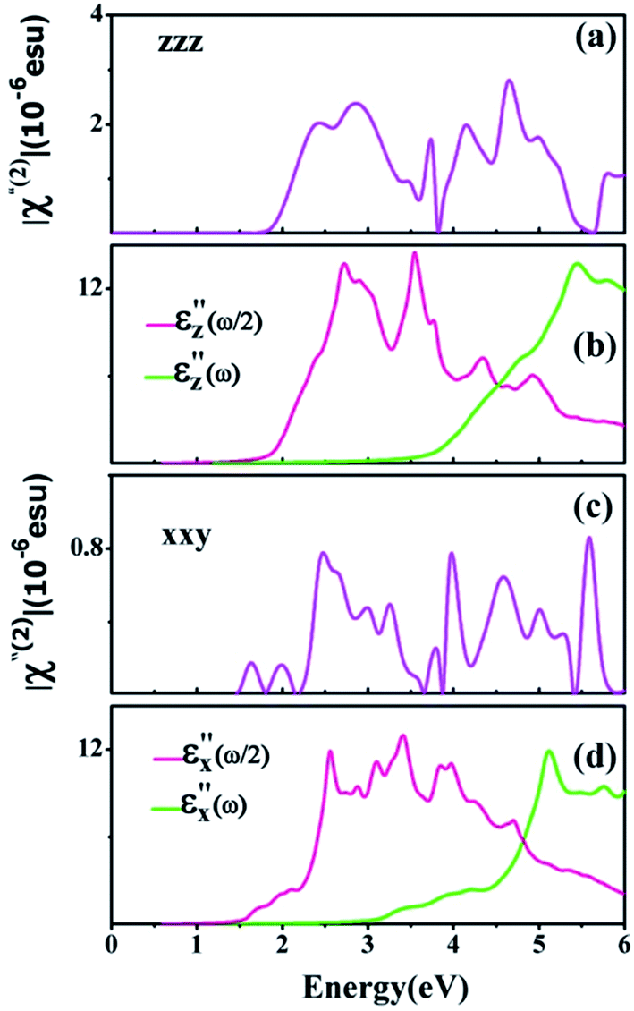 | ||
| Fig. 6 (a) Absolute value of the imaginary part of χ(2)zzz(−2ω,ω,ω), (b) imaginary part of the dielectric function ε′′z as a function of ω/2 and ω, (c) absolute value of the imaginary part of χ(2)xxy(−2ω,ω,ω), and (d) imaginary part of the dielectric function ε′′x as a function of ω/2 and ω of monolayer α-Ga2S3. | ||
As shown in Table 1, the HSE06 bandgaps of few-layer α-Ga2S3 are in the visible range. In contrast, the HSE06 bandgaps of few-layer α-In2Se3 and AAA α-Ga2S3 are much narrower, which promises low laser damage thresholds. Therefore, we focus on SHG properties of bilayer AA and AB, and ABA α-Ga2S3, and their real and imaginary parts of χ(2)zzz(−2ω,ω,ω), χ(2)zxx(−2ω,ω,ω) and χ(2)xxy(−2ω,ω,ω) are displayed in Fig. 7. The line shape of the three SHG spectra of AA α-Ga2S3 is very similar to that of monolayer α-Ga2S3, and the SHG spectra of AA are significantly redshifted in comparison with that of monolayer α-Ga2S3 because of the sizable bandgap reduction. Moreover, the calculated χ(2)zzz(0), χ(2)zxx(0) and χ(2)xxy(0) of AA α-Ga2S3 are very close to those of monolayer α-Ga2S3, respectively. These suggest that optical transitions occur within each α-Ga2S3 layer, namely the SHG property of each α-Ga2S3 layer is not modified by the built-in electric field of the neighboring α-Ga2S3 layer. According to the electric dipole theory, the SHG intensity shows a quadratic dependence on the SHG coefficient and the layer thickness,4 and thereby the non-resonant SHG intensity in bilayer AA is about four times that in monolayers.
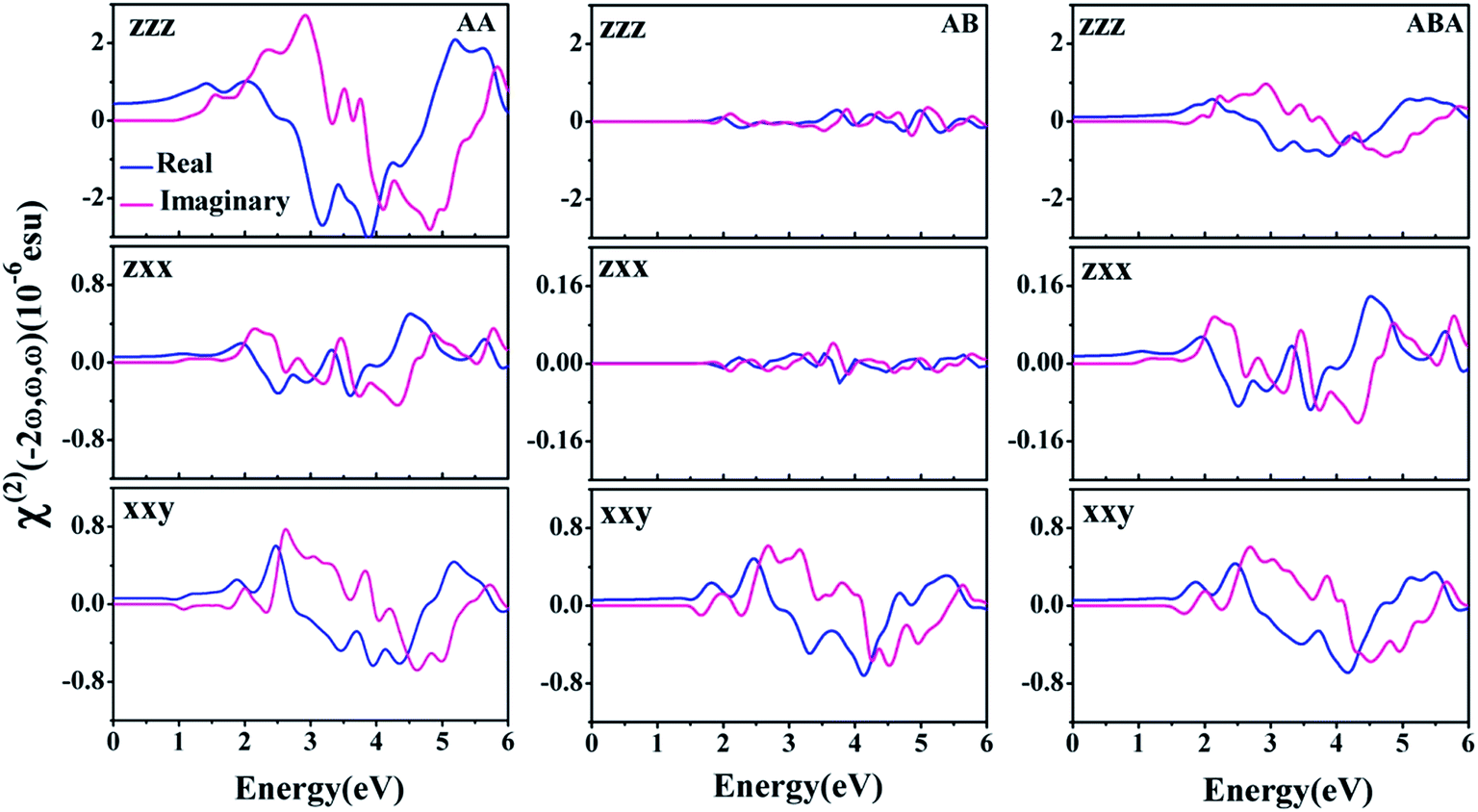 | ||
| Fig. 7 Calculated real and imaginary parts of SHG coefficients χ(2)zzz(−2ω,ω,ω), χ(2)zxx(−2ω,ω,ω) and χ(2)xxy(−2ω,ω,ω) of bilayer AA, AB, and trilayer ABA α-Ga2S3. | ||
The redshift of χ(2)xxy(−2ω,ω,ω) for AB α-Ga2S3 is negligible as the bandgap difference of monolayers and AB is small. χ(2)zzz(−2ω,ω,ω) and χ(2)zxx(−2ω,ω,ω) of AB α-Ga2S3 nearly vanishes, which is further corroborated by its vanishing static χ(2)zzz(0) and χ(2)zxx(0). The electric dipole in the z(x) direction of the top and bottom α-Ga2S3 layers in bilayer AB points oppositely, and accordingly their contribution to the static χ(2)zzz(0)(χ(2)zxx(0)) cancels each other. The electric dipole in the z direction is the out-of-plane electric dipole, while the electric dipole in the x direction is the in-plane electric dipole. The χ(2)zzz(−2ω,ω,ω) component of trilayer ABA α-Ga2S3 is 1/3 that of monolayer α-Ga2S3 as the contribution of the middle and bottom layers to χ(2)zzz(−2ω,ω,ω) in trilayer ABA cancels each other. Therefore, we propose that one can effectively tune the out-of-plane SHG coefficient by switching the electric dipole orientation in 2D nanosheets. Additionally, we summarize χ(2)(0) of AB and ABA α-In2Se3 in Table 1, which indicates the obtained optical rules are valid for other α-M2X3 nanosheets. The SHG property of few-layer α-In2Se3 in recent experiments could be obtained by analogy.16
3.4. Piezoelectric properties
To obtain piezoelectric strain coefficients dij which measure mechanical–electrical energy conversion ratios, we calculate elastic constants Cij and piezoelectric stress coefficients eij using density functional perturbation theory (DFPT).46 The clamped-ion elastic and piezoelectric coefficients are obtained from purely electronic contributions, while the relaxed-ion coefficients are obtained from the sum of electronic and ionic contributions. The relaxed-ion elastic and piezoelectric coefficients are physically meaningful and can be directly compared with experimental results. As shown in Table 2, single- and few-layer α-M2X3 have three independent elastic constants: C11, C12 and C66. The calculated clamped-ion and relaxed-ion elastic constants follow the correlation of C66 ≈ (C11 − C12)/2. The relaxed-ion elastic constants fulfil the Born criteria of stability of 2D hexagonal structures,47–49 i.e. C11 > 0 and C11–C12 > 0, ensuing these monolayers and few-layers are mechanically stable. The calculated relaxed-ion Young's moduli (Y = (C112 − C122)/C11) of single-layer α-M2X3 are smaller than that of graphene (341 N m−1) and monolayer BN (275.9 N m−1),50 and comparable with that of monolayer TMDCs.51 Therefore, α-M2X3 monolayers are much softer than graphene and monolayer BN, and their stiffness is comparable with that of monolayer TMDCs. Moreover, the calculated Young's moduli of bilayer (trilayer) α-Ga2S3 are about two (three) times that of monolayer α-Ga2S3. This is because, of the same strain, the force needed for bilayers (trilayers) is two (three) times that of monolayers.| Clamped-ion | Relaxed-ion | ||||||||
|---|---|---|---|---|---|---|---|---|---|
| C11 | C12 | C66 | Y | C11 | C12 | C66 | Y | ||
| α-Ga2S3 | ML | 146.7 | 48.6 | 48.9 | 130.5 | 115.5 | 45.0 | 35.1 | 104.3 |
| AA | 293.3 | 97.6 | 97.6 | 261.0 | 228.2 | 83.3 | 72.4 | 197.7 | |
| AB | 292.3 | 96.2 | 97.6 | 260.6 | 224.3 | 85.4 | 69.3 | 191.7 | |
| ABA | 439.2 | 145.8 | 146.7 | 390.7 | 348.7 | 134.5 | 106.6 | 296.8 | |
| AB | |||||||||
| ab | |||||||||
| α-Ga2Se3 | ML | 120.9 | 39.9 | 40.2 | 107.7 | 91.8 | 42.0 | 24.6 | 72.5 |
| α-In2S3 | ML | 117.0 | 43.2 | 36.6 | 101.0 | 75.6 | 36.6 | 19.2 | 57.8 |
| α-In2Se3 | ML | 96.3 | 35.1 | 30.6 | 83.5 | 68.4 | 24.0 | 21.9 | 59.9 |
Single- and few-layer α-M2X3 have two independent piezoelectric stress coefficients e11 and e31 dictated by C3v symmetry. The piezoelectric strain coefficients d11 and d31, which respectively measure the mechanical–electrical energy conversion ratios in x and z directions, are expressed as d11 = e11/(C11 − C12) and d31 = e31/(C11 + C12).12 The relaxed-ion e11 values of monolayer α-Ga2S3 and α-Ga2Se3 in Fig. 8(a) are even larger than that of monolayer 2H-CrTe2, which has the largest e11 of 654 pC m−1 among TMDCs.12 The relaxed-ion d11 values of single-layer α-Ga2Se3 and α-In2Se3 in Fig. 8(c) are comparable with the maximum d11 of 13.45 pm V−1 for monolayer TMDCs, and larger than the maximum d11 of 8.47 pm V−1 for Janus group-III chalcogenide monolayers.11 The relaxed-ion d11 values of α-In2S3 and α-In2S3 monolayers are comparable with the maximum d11 of 2.30 pm V−1 for group-III chalcogenides.10 Therefore, α-M2X3 monolayers are promising in ultrathin piezoelectric sensors and nano-generators. Fig. 8(a) and (c) further suggest the electronic and ionic polarizations of α-Ga2S3 and α-Ga2Se3 monolayers both positively contribute to relaxed-ion piezoelectric coefficients e11 and d11, resulting in significant in-plane piezoelectricity. In contrast, the electronic and ionic polarizations of α-In2S3 and α-In2Se3 monolayers oppositely contribute to relaxed-ion e11 and d11, resulting in smaller in-plane piezoelectricity. Our calculation also generates relaxed-ion e11 and d11 are respectively 369 pC m−1 and 3.72 pm V−1 for monolayer MoS2, in good agreement with previous theoretical values of 364 pC m−1 and 3.73 pm V−1,8 indicating our theoretical results are numerically reliable.
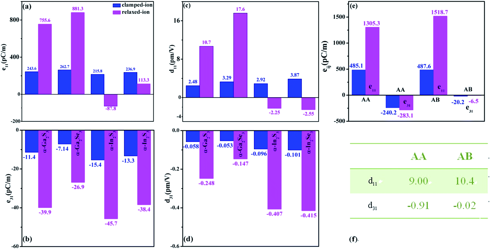 | ||
| Fig. 8 Piezoelectric coefficients (a) e11, (b) e31, (c) d11 and (d) d31 of monolayer α-M2X3 in clamped- and relaxed-ion cases. (e) Clamped- and relaxed-ion e11 and e31 of bilayer AA and AB α-Ga2S3. (f) Relaxed-ion d11 and d31 (pm V−1) of AA and AB α-Ga2S3. | ||
Fig. 8(b) and (d) suggest α-M2X3 monolayers have nonzero out-of-plane piezoelectric coefficients e31 and d31. The electronic and ionic polarizations of all α-M2X3 monolayers both negatively contribute to e31 and d31. The d31 values of α-M2X3 monolayers are comparable with the maximum d31 of 0.46 pm V−1 for monolayer Janus group-III chalcogenides11 and the maximum d31 of 0.658 pm V−1 for bucked hexagonal compounds.12 However, the bucked hexagonal compounds are energetically metastable. In contrast, α-M2X3 monolayers are energetically, dynamically25 and mechanically stable, ensuing they are experimentally feasible.
The calculated piezoelectric coefficients e11 and e31 of AA and AB α-Ga2S3 are summarized in Fig. 8(e), while their d11 and d31 coefficients are displayed in Fig. 8(f). Comparisons of Fig. 8(a) and (e) show the clamped-ion (relaxed-ion) e11 of AB α-Ga2S3 is exactly twice that of monolayer α-Ga2S3. This is because, of the same strain, the change of polarization charges in the x direction of bilayer AB α-Ga2S3 is twice that of monolayer α-Ga2S3. Therefore, the piezoelectric effect occurs within each α-Ga2S3 layer in AB, namely the piezoelectricity of each α-Ga2S3 layer is not modified by the built-in electric field of the neighboring α-Ga2S3 layer. This is further affirmed by the relaxed-ion d11 of 10.4 pm V−1 for AB α-Ga2S3 being very close to that (10.7 pm V−1) for monolayer α-Ga2S3. The relaxed-ion d31 of bilayer AB nearly vanishes since the piezoelectric contribution to d31 of each α-Ga2S3 layer cancels each other.
Fig. 8(a) and (e) further suggest the clamped-ion e11 of 485.1 pC m−1 for bilayer AA α-Ga2S3 is exactly twice that (243.6 pC m−1) of monolayer α-Ga2S3, while the relaxed-ion e11 of 1350.3 pC m−1 for AA α-Ga2S3 is to some extent smaller than twice that (755.6 pC m−1) of monolayer α-Ga2S3. The clamped-ion e31 of −240.2 pC m−1 for AA α-Ga2S3 is much larger than that (−11.4 pC m−1) of monolayer α-Ga2S3, namely the clamped-ion e31 of AA α-Ga2S3 is much enhanced by the strong built-in electric field originated from the parallel out-of-plane electric polarizations of α-Ga2S3 layers. The relaxed-ion d31 of −0.91 pm V−1 for AA α-Ga2S3 is accordingly several times larger than that (−0.248 pm V−1) of monolayer α-Ga2S3, suggesting AA α-Ga2S3 is much more easily polarized than monolayer α-Ga2S3. Similarly, the electric dipole (0.165 eÅ) of AA α-In2Se3 is much larger than that (0.07 eÅ) of monolayer α-In2Se3.25
Briefly, we find AA α-Ga2S3 has the largest out-of-plane d31 among all atomic-thick 2D materials up to date. More importantly, the built-in electric field can induce strong out-of-plane piezoelectricity in atomic-thick 2D materials, which is corroborated by a recent calculation which finds large d31 of −1.234 pm V−1 and d33 of −13.517 pm V−1 in multilayer MoSTe.15 However, the large d33(∂P3/∂σ3, P is the electric polarization and σ is the stress) in multilayer MoSTe will vanish in atomic-thick 2D MoSTe such as monolayer15 and bilayer MoSTe (cf. ESI-4†). This reflects it is very difficult to impose stresses along the z direction for atomic-thick 2D materials since their effective thickness is far smaller than their flake size. For instance, the effective thickness of monolayer MoSSe is about 6.3 Å while its flake size is more than 5 μm.52 The effective thickness of monolayer MoSSe is considered as the average of that of MoS2 and MoSe2 monolayers.35 In contrast, it is easy to impose stresses along the x direction to achieve large d31(∂P3/∂σ1) because of the large size of atomic-thick 2D materials. Therefore, it is more reasonable to induce out-of-plane piezoelectricity by imposing stresses along the x direction within atomic-thick 2D materials. Moreover, the d31 coefficient of −1.234 pm V−1 for multilayer MoSTe decreases to −0.417 pm V−1 of bilayer MoSTe (cf. ESI-4†), being smaller than that of AA Ga2S3. The small bandgap of AAA α-Ga2S3 is disadvantageous to avoid current leakages. The piezoelectric coefficient d11 of ABA α-Ga2S3 should be close to that of monolayer α-Ga2S3, while its d31 coefficient is around 1/3 that of monolayer α-Ga2S3 since the piezoelectric response occurs within each α-Ga2S3 layer.
4. Summaries
We have carried out first-principles calculations of structural, electronic, SHG and piezoelectric properties of single- and few-layer α-M2X3 (M = Ga, In; X = S, Se). Firstly, α-M2X3 few-layers are energetically favorable and mechanically stable, ensuring bilayer AA and trilayer AAA can be successfully attained by mechanical exfoliation and bilayer AB and trilayer ABA can be achieved by switching the electric dipole orientation. Secondly, the relative flat top valence band of α-M2X3 monolayer promises large SHG coefficients, and their large bandgaps are helpful to avoid current leakages in piezoelectric devices. The splitting of energy bands in few-layer AA and AAA is very pronounced because of the built-in electric field originated from the parallel out-of-plane electric dipoles, while in contrast, that of AB and ABA is not pronounced because the built-in electric field significantly diminishes as the out-of-plane electric dipoles are antiparallelly aligned. Therefore, we propose a completely new method, i.e. switching the electric dipole orientation to tune electronic structures and bandgaps, which is very advantageous to tune the sensing photon energy window and achieve the semiconducting nature. Thirdly, the in-plane SHG coefficients of α-M2X3 monolayers are comparable with that of AgGaS2 crystals. More importantly, we find out-of-plane SHG in α-M2X3 monolayers and their out-of-plane SHG coefficients are comparable with that of GaAs crystals. Furthermore, SHG occurs within each α-M2X3 layers in AA and AB, and accordingly one can achieve an enhanced out-of-plane SHG intensity in AA and eliminate the out-of-plane SHG in AB. Fourthly, the stiffness of α-M2X3 monolayers is comparable that with monolayer TMDCs. α-M2X3 monolayers exhibit strong in-plane and considerable out-of-plane piezoelectricity. Furthermore, out-of-plane piezoelectricity vanishes in AB α-Ga2S3, and it is greatly enhanced in AA α-Ga2S3 as the electric dipoles are parallelly aligned. To our knowledge, out-of-plane SHG in 2D materials has been rarely reported, while the out-of-plane piezoelectricity is very limited in ultrathin 2D materials. Here we have presented strong out-of-plane SHG and piezoelectricity in ultrathin 2D materials. In general, our research will stimulate researches on the ultrathin 2D photo detection, SHG and piezoelectric devices.Conflicts of interest
There are no conflicts to declare.Acknowledgements
This work is supported by National Nature Science foundation of China (21373099, 21573090), Jilin Province Science and Technology Development Plan (20150101005JC) and the Ministry of Education of China (20130061110020). We also thank professor Yong-Fan Zhang in Fuzhou University for SHG calculation program developing.References
- D. Neshev and Y. Kivshar, Science, 2014, 344, 483 CrossRef CAS PubMed.
- X. Yin, Z. Ye, D. A. Chenet, Y. Ye, K. O'Brien, J. C. Hone and X. Zhang, Science, 2014, 344, 488 CrossRef CAS PubMed.
- W. Jie, X. Chen, D. Li, L. Xie, Y. Y. Hui, S. P. Lau, X. Cui and J. Hao, Angew. Chem., Int. Ed., 2015, 54, 1185 CrossRef CAS PubMed.
- X. Zhou, J. Cheng, Y. Zhou, T. Cao, H. Hong, Z. Liao, S. Wu, H. Peng, K. Liu and D. P. Yu, J. Am. Chem. Soc., 2015, 137, 7994 CrossRef CAS PubMed.
- I. J. Wu and G. Y. Guo, Phys. Rev. B: Condens. Matter Mater. Phys., 2008, 78, 035447 CrossRef.
- G. Y. Guo and J. C. Lin, Phys. Rev. B: Condens. Matter Mater. Phys., 2005, 72, 075416 CrossRef.
- L. Hu and D. S. Wei, Phys. Chem. Chem. Phys., 2017, 19, 2235 RSC.
- K. A. N. Duerloo, M. T. Ong and E. J. Reed, J. Phys. Chem. Lett., 2012, 3, 2871 CrossRef CAS.
- H. Zhu, Y. Wang, J. Xiao, M. Liu, S. Xiong, Z. J. Wong, Z. Ye, Y. Ye, X. Yin and X. Zhang, Nat. Nanotechnol., 2015, 10, 151 CrossRef CAS PubMed.
- W. Li and J. Li, Nano Res., 2015, 8, 3796 CrossRef CAS.
- Y. Guo, S. Zhou, Y. Bai and J. Zhao, Appl. Phys. Lett., 2017, 110, 163102 CrossRef.
- M. N. Blonsky, H. L. Zhuang, A. K. Singh and R. G. Hennig, ACS Nano, 2015, 9, 9885 CrossRef CAS PubMed.
- M. T. Ong and E. J. Reed, ACS Nano, 2012, 6, 1387 CrossRef CAS PubMed.
- W. Wu, L. Wang, Y. Li, F. Zhang, L. Lin, S. Niu, D. Chenet, X. Zhang, Y. Hao, T. F. Heinz, J. Hone and Z. L. Wang, Nature, 2014, 514, 470 CrossRef CAS PubMed.
- L. Dong, J. Lou and V. B. Shenoy, ACS Nano, 2017, 11, 8242 CrossRef CAS PubMed.
- Y. Zhou, D. Wu, Y. Zhu, Y. Cho, Q. He, X. Yang, K. Herrera, Z. Chu, Y. Han, M. C. Downer, H. Peng and K. Lai, Nano Lett., 2017, 17, 5508 CrossRef CAS PubMed.
- S. Zhou, X. Tao and Y. Gu, J. Phys. Chem. C, 2016, 120, 4753 CAS.
- X. Tao and Y. Gu, Nano Lett., 2013, 13, 3501 CrossRef CAS PubMed.
- G. Almeida, S. Dogan, G. Bertoni, C. Giannini, R. Gaspari, S. Perissinotto, R. Krahne, S. Ghosh and L. Manna, J. Am. Chem. Soc., 2017, 139, 3005 CrossRef CAS PubMed.
- R. B. Jacobs-Gedrim, M. Shanmugam, N. Jain, C. A. Durcan, M. T. Murphy, T. M. Murray, R. J. Matyi, R. L. Moore and B. Yu, ACS Nano, 2014, 8, 514 CrossRef CAS PubMed.
- W. Feng, W. Zheng, F. Gao, X. Chen, G. Liu, T. Hasan, W. Cao and P. Hu, Chem. Mater., 2016, 28, 4278 CrossRef CAS.
- D. Wu, A. J. Pak, Y. Liu, Y. Zhou, X. Wu, Y. Zhu, M. Lin, Y. Han, Y. Ren, H. Peng, Y. Tsai, G. S. Hwang and K. Lai, Nano Lett., 2015, 15, 8136 CrossRef CAS PubMed.
- J. Quereda, R. Biele, G. Rubio-Bollinger, N. Agraït, R. D'Agosta and A. Castellanos-Gomez, Adv. Opt. Mater., 2016, 4, 1939 CrossRef CAS.
- L. Debbichi, O. Eriksson and S. Lebègue, J. Phys. Chem. Lett., 2015, 6, 3098 CrossRef CAS PubMed.
- W. Ding, J. Zhu, Z. Wang, Y. Gao, D. Xiao, Y. Gu, Z. Zhang and W. Zhu, Nat. Commun., 2017, 8, 14956 CrossRef CAS PubMed.
- H. Wang and X. Qian, Nano Lett., 2017, 17, 5027 CrossRef CAS PubMed.
- L. Hu, X. R. Huang and D. S. Wei, Phys. Chem. Chem. Phys., 2017, 19, 11131 RSC.
- P. E. Blöchl, Phys. Rev. B: Condens. Matter Mater. Phys., 1994, 50, 17953 CrossRef.
- G. Kresse and J. Furthmüller, Phys. Rev. B: Condens. Matter Mater. Phys., 1996, 54, 11169 CrossRef CAS.
- G. Kresse and J. Furthmüller, Comput. Mater. Sci., 1996, 6, 15 CrossRef CAS.
- G. Kresse and J. Hafner, Phys. Rev. B: Condens. Matter Mater. Phys., 1993, 47, 558 CrossRef CAS.
- G. Kresse and J. Hafner, Phys. Rev. B: Condens. Matter Mater. Phys., 1994, 49, 14251 CrossRef CAS.
- J. P. Perdew, K. Burke and M. Ernzerhof, Phys. Rev. Lett., 1996, 77, 3865 CrossRef CAS PubMed.
- S. Grimme, J. Comput. Chem., 2006, 27, 1787 CrossRef CAS PubMed.
- C. Y. Wang and G. Y. Guo, J. Phys. Chem. C, 2015, 119, 13268 Search PubMed.
- H. L. Zhuang and R. G. Hennig, Chem. Mater., 2013, 25, 3232 CrossRef CAS.
- C. Aversa and J. E. Sipe, Phys. Rev. B: Condens. Matter Mater. Phys., 1995, 52, 14636 CrossRef CAS.
- S. N. Rashkeev, W. R. L. Lambrecht and B. Segall, Phys. Rev. B: Condens. Matter Mater. Phys., 1998, 57, 3905 CrossRef CAS.
- Z. Fang, J. Lin, R. Liu, P. Liu, Y. Li, X. Huang, K. Ding, L. Ning and Y. Zhang, CrystEngComm, 2014, 16, 10569 RSC.
- M. Grüning and C. Attaccalite, Phys. Rev. B: Condens. Matter Mater. Phys., 2014, 89, 081102 CrossRef.
- H. C. Hsueh, G. Y. Guo and S. G. Louie, Phys. Rev. B: Condens. Matter Mater. Phys., 2011, 84, 085404 CrossRef.
- F. Karlický and M. Otyepka, Ann. Phys., 2014, 526, 408 CrossRef.
- Y. Li, Y. Rao, K. F. Mak, Y. You, S. Wang, C. R. Dean and T. F. Heinz, Nano Lett., 2013, 13, 3329 CrossRef CAS PubMed.
- L. Bai, Z. Lin, Z. Wang, C. Chen and M. H. Lee, J. Chem. Phys., 2004, 120, 8772 CrossRef CAS PubMed.
- Z. Ma, K. Wu, R. Sa, Q. Li and Y. Zhang, J. Alloys Compd., 2013, 568, 16 CrossRef CAS.
- X. Wu, D. Vanderbilt and D. R. Hamann, Phys. Rev. B: Condens. Matter Mater. Phys., 2005, 72, 035105 CrossRef.
- H. L. Zhuang, M. D. Johannes, M. N. Blonsky and R. G. Hennig, Appl. Phys. Lett., 2014, 104, 022116 CrossRef.
- M. Born and H. Huang, Dynamical Theory of Crystal Lattices, Clarendon Press, Oxford, 1954 Search PubMed.
- F. Mouhat and F. X. Coudert, Phys. Rev. B: Condens. Matter Mater. Phys., 2014, 90, 224104 CrossRef.
- D. Çakır, F. M. Peeters and C. Sevik, Appl. Phys. Lett., 2014, 104, 203110 CrossRef.
- M. M. Alyörük, Y. Aierken, D. Çakır, F. M. Peeters and C. Sevik, J. Phys. Chem. C, 2015, 119, 23231 Search PubMed.
- J. Zhang, S. Jia, I. Kholmanov, L. Dong, D. Er, W. Chen, H. Guo, Z. Jin, V. B. Shenoy, L. Shi and J. Lou, ACS Nano, 2017, 11, 8192 CrossRef CAS PubMed.
Footnote |
| † Electronic supplementary information (ESI) available. See DOI: 10.1039/c7ra11014f |
| This journal is © The Royal Society of Chemistry 2017 |