
 Open Access Article
 This Open Access Article is licensed under a
 Creative Commons Attribution 3.0 Unported Licence
Si nanorod arrays modified with metal–organic segments as anodes in lithium ion batteries†
Yingjian Yuac,
Chuang Yuea,
Yingzi Hanb,
Chuanhui Zhangb,
Mingsen Zheng b,
Binbin Xub,
Shuichao Lin*b,
Jing Li*a and
Junyong Kanga
b,
Binbin Xub,
Shuichao Lin*b,
Jing Li*a and
Junyong Kanga
aCollaborative Innovation Center for Optoelectronic Semiconductors and Efficient Devices, Department of Physics/Pen-Tung Sah Institute of Micro-Nano Science and Technology, Xiamen University, Xiamen, Fujian 361005, China. E-mail: lijing@xmu.edu.cn
bState Key Lab of Physical Chemistry of Solid Surfaces, College of Chemistry and Chemical Engineering, Xiamen University, Xiamen, Fujian 361005, China. E-mail: sclin@xmu.edu.cn
cDepartment of Physics Science and Technology, Kunming University, Kunming, Yunnan 650217, China
First published on 22nd November 2017
Abstract
Metal–organic segments (MOSs) have been controllably synthesized to composite with Si nanorod (NR) arrays as electrodes in lithium ion batteries (LIBs). These kinds of MOSs are suggested to be derived from solution species such as [Zn(C4H6N2)Ac]+, [Zn(C4H6N2)2Ac]+ and [Zn(C3H4N2)(C4H6N2)Ac]+ as detected by electrospray ionization time-of-flight mass spectrometry (ESI-TOF-MS). It is found that solution concentration and growth time have significant effects on the MOS coating around Si NRs. The uniform coating of MOSs around Si NRs has been successfully produced at relatively low solution concentrations or for shorter growth time, which was proved to be helpful to enhance the capacity of the composite electrode up to ∼1.1 mA h cm−2 at a current density of 10 μA cm−2 and ∼0.5 mA h cm−2 on increasing the current density to 50 μA cm−2. Furthermore, at an even higher current density of 200 μA cm−2 (vs. initial 10 μA cm−2) the composite electrodes still can maintain more than 50% of the initial capacities. While, given a higher solution concentration or longer reaction time, large ZIF-61 crystals, a kind of metal–organic framework (MOF), would form on the top of Si NRs. Unlike MOSs, large ZIF-61 crystals fail to cover the Si NR homogeneously, and consequently the capacities of ZIF-61/Si NR composite electrodes are much lower than those of MOS/Si NR electrodes. This work not only demonstrates a simple method for Si surface modification to enhance its corresponding electrochemical performance, but also provides a potential general strategy for the coating of different surfaces by the cross-linking of metal nodes and organic ligands.
Introduction
Given their long working life and high energy/power density, LIBs have been widely investigated, with focus on electrode materials and configurations et al.1–3 Meanwhile, micro-LIBs are attracting increasing attention due to the fast growth of micro/nano-electro-mechanical system (M/NEMS) techniques.4,5 Si, with the feasible integration with electronic devices, not to mention its high theoretical capacity of ∼4200 mA h g−1 and low potential plateau at 0.5 V as an anode material, has been initially applied in LIBs and micro-LIBs.6–8 In order to address the volume expansion (>300%) issue of the Si anode during cycling processes,9,10 nanostructures like nanowires (NWs)11–18 and surface coating layers19–35 such as graphene, pyrolytic carbon, carbon nanotubes and Ge are often utilized. However, during generating the carbon coatings, thermal decomposition may cause the release of CO, CO2, and volatile organic compounds and changes in active material structures sometimes.36,37 While for coatings like Ge, it may be inevitable to use high-cost precursors like GeH4 (ref. 18 and 38) and complicated instruments such as ultra-high vacuum chemical vapor deposition (UHVCVD).39–41 So, feasible, efficient and low-cost strategies are still in demand for the modification of Si surfaces as well-performed anodes in LIBs or micro-LIBs.Metal–organic frameworks (MOFs) have been researched as electrodes for LIBs in recent years.39,42–47 However, some MOFs' inherent crystalline properties restraint their uniform fabrications on the Si NWs.48
Herein, a feasible method was developed to fabricate the metal–organic segments (MOSs) homogeneously covering around the Si nanorods (NRs) as anodes in LIBs or micro-LIBs. The MOS/Si NRs electrode was fabricated by inductive coupled plasma (ICP) dry etching followed by a solution growth process. It is found that the morphologies of MOSs vary by the synthesis conditions like solution concentrations and growth time. At relatively low solution concentrations or for shorter growth time, the uniform coating of MOSs around Si NRs was produced; for comparison, given a higher solution concentration or longer reaction time, large ZIF-61 crystals would form on the top of Si NRs. Furthermore, by the characterizations of transmission electron microscope (TEM) and ESI-TOF-MS, the growth mechanisms of MOSs were demonstrated, which would provide guidelines for the growth of other MOSs-like materials. With the uniform coating of MOSs around Si NRs, the corresponding promising electrochemical characteristics were accomplished. This work proposed a convenient strategy to fabricate nanostructured Si-based composite electrode by the cross-linking of metal nodes and organic ligands, which would facilitate the applications of MOS or other MOF-like materials in lithium ion batteries without the pyrolysis process or the introduction of conducting layers.
Experimental section
Fabrication of MOS/Si NRs
As shown in Scheme 1, polystyrene (PS) template method followed by the inductive coupled plasma (ICP) etching was conducted to prepare Si NR arrays by referring to our previous work.39 After the prepared Si NR arrays were immersed in a 50 mL mixed solution containing 2-methylimidazole and imidazole with proper concentrations, the 25 mL Zn(Ac)2·2H2O solution was added and the mixed solution was kept at 20 °C for 4–24 h to fabricate MOS/Si NRs. The prepared MOS/Si composite NRs were rinsed by methanol and dried. | ||
| Scheme 1 Fabrication processes for the MOS/Si NR arrays: (i) ICP Etching to fabricate Si NR Arrays, (ii) template removal by washing, and (iii) growth of MOS around Si NR arrays by the solution growth. | ||
Characterization
The morphologies of MOS/Si NRs were investigated by the SU70 scanning electron microscope (SEM). The high-resolution (HR) transmission electron microscope (TEM) images were visualized by JEM-2100 HRTEM and the elemental analyses were realized by Tecnai F30 TEM.The 10 × 10 mm2 pieces of Si NR substrates with the Cr/Au current collector were prepared for the electrochemical measurements. The 20/200 nm Cr/Au were deposited on the back side of the substrates by magnetron sputtering (JC-500-3/D) for 1.5/7 min at powers of 360/420 W. The Si, MOS/Si and ZIF-61/Si NRs were then assembled in coin cells (2025) for testing the corresponding cycling and rate abilities.39 Specifically, the coin cells consisted of lithium foils (counter electrodes), Celgard 2400 microporous film (separator), LiPF6 (electrolyte) and Si-based NR pieces (working electrodes). The tests for electrochemical properties of the coin cells were conducted on the electrochemical workstation (CHI660D) and Land CT2001A battery test system. As well known, the properties of micro-LIBs are usually evaluated by energy or power densities in a unit area or volume. So, the areal capacity (μA h cm−2) was applied to discuss the lithium storage ability of the composite electrodes in this work.
Results and discussions
Different solution concentrations and reaction time were conducted to modify the surface of Si NRs, as visualized in Fig. 1 and 2. When the lower solution concentrations of 2-methylimidazole, imidazole and Zn(Ac)2·2H2O at 1.2 mmol L−1, 1.2 mmol L−1 and 0.6 mmol L−1 respectively were employed, with the reaction time of 4 h, no apparent change can be found around Si NR arrays compared with the only Si NRs as seen in Fig. S1,† except for the unconspicuous particle-like coating formed on Si NRs' side walls as displayed in Fig. 1a. This particle-like coating was lacking in crystallinity characterized within the detection limit of X-ray diffraction (XRD) pattern, which was then named as metal–organic segments (MOSs). It should be noted that the “segments” often represents the metal–organic complexes presenting during the growth of MOFs or parts of synthesized MOFs.49,50 While, MOFs usually refer to crystals consisting of metal nodes coordinated to organic ligands.51 So, here, the definition of “metal–organic segments (MOSs)” may include both an amorphous coating layer and tiny ZIF-61 particles around Si NRs, which share the similar basic units of metal–organic complexes. Further verification will be demonstrated in the following. Further, after a 6 hour reaction, these tiny particles grew visibly. And expectably, the quantity of the particles increased apparently after the reaction time of 12 h. The corresponding energy dispersive X-ray (EDX) spectrum exhibited in Fig. S2† identifies the C, N, Zn, Si elements, indicating the successful fabrication of MOSs around Si NRs. Dramatically, the tiny particles disappeared after a 24 hour growth process; however, a large number of ZIF-61 crystals with dimensions of several micrometers formed on the top of Si NRs as shown in Fig. S3,† further identified by the X-ray diffraction (XRD) pattern51 as seen in Fig. S4.† Additionally, the similar phenomenon also happened when the solution concentrations of 2-methylimidazole, imidazole and Zn(Ac)2·2H2O were increased to 3.0 mmol L−1, 3.0 mmol L−1 and 1.5 mmol L−1, respectively, as exhibited in Fig. 2. In these higher concentration cases, when the growth time is 4 h, more tiny particles appeared than those in the above samples synthesized at the lower solution concentrations, indicating the positive correlation of solution concentration to the MOS coating. At the higher solution concentration, the quantities of the raw materials such as 2-methylimidazole, imidazole and Zn(Ac)2·2H2O are sufficient. So, it is easier to collect enough molecules and ions on the surface of Si NRs, and faster to form the MOS coating. After the 6 hour growth, the quantity of tiny particles decreases; however, large crystals can be found on the top of the Si NRs as seen in Fig. S5a.† Consequently, tiny particles almost disappear after the 12 hour reaction and similarly large numbers of ZIF-61 crystals were produced as shown in Fig. S5b.† The barely characterized elements of Zn and N on the sidewalls of those Si NRs after a 12 hour growth process, as seen in the EDX pattern of Fig. S6,† evidenced the dissolution of MOSs around the Si NRs. According to the above phenomena, at the initial stage of the growth, the coating of MOS on Si NRs would be denser as the reactions proceeded; however, the MOS would dissolve after a certain reaction time and larger ZIF-61 crystals would gradually form similarly as the Ostwald ripening.52 | ||
| Fig. 1 Vertical-view and lateral-view SEM images of various MOS/Si NRs fabricated by 1.2 mmol L−1 2-methylimidazole, 1.2 mmol L−1 imidazole and 0.6 mmol L−1 Zn(Ac)2·2H2O with growth time of (a and b) 4 h, (c and d) 6 h, (e and f) 12 h, and (g and h) 24 h. | ||
 | ||
| Fig. 2 Vertical-view and lateral-view SEM images of various MOS/Si NRs fabricated by 3.0 mmol L−1 2-methylimidazole, 3.0 mmol L−1 imidazole and 1.5 mmol L−1 Zn(Ac)2·2H2O with growth time of (a and b) 4 h, (c and d) 6 h, and (e and f) 12 h. | ||
More configuration details of the MOS/Si composite NR fabricated at the lower concentration for 12 h are visualized by TEM characterizations as seen in Fig. 3. An individual MOS/Si NR is presented in Fig. 3a, in which crystalline Si inner core is evidently coated by the amorphous layer with some tiny crystalline ZIF-61 particles as shown in Fig. 3b. Its corresponding elemental mappings were also characterized as seen in Fig. 3c, identifying the Si, N, and Zn elements and further evidencing the successful fabrication of the MOS/Si NRs. Therefore, it can be proposed that amorphous layer was first synthesized to adhere around the Si NRs and afterwards some tiny crystalline ZIF-61 were produced in the MOS layer.
 | ||
| Fig. 3 (a) TEM image of an individual MOS/Si NR fabricated at the lower concentration for 12 h; (b) HRTEM images of the interface between Si and MOS with dotted lines showing the (055) plane of tiny crystalline ZIF-61 particles; (c) dark-field TEM image of the MOS/Si NR with relevant elemental EDX mappings of Si K line (i), N K line (ii) and Zn L line (iii). | ||
To clarify the growth processes and structures of MOS, a representative spectrum of full range of positively charged molecular species detected using ESI-TOF-MS is exhibited in Fig. 4a, with their quantities shown in Fig. 4b. The samples were fabricated at the lower concentration for 12 h. Among them, Zn1 series (ligands coordination to one Zn ion) such as [Zn(C4H6N2)Ac]+, [Zn(C4H6N2)2Ac]+ and [Zn(C3H4N2)(C4H6N2)Ac]+ are the majority, which could consequently form the higher oligomers in different coordinations.53 These complexes are the basic structural unit in MOSs adhered around the Si NRs. Along with the undergoing of reactions, some oligomers tend to arrange in a certain order to form the tiny crystalline ZIF-61 particles as shown in Fig. 3b.54 However, larger crystals are more energetically favored than smaller particles stemming from the fact that molecules on the surface of a particle are less stable than the ones in the interior.52 Therefore, the MOS layer with larger interfacial energy is inclined to dissolve and form larger ZIF-61 crystals on the top of the Si NRs to decrease total energy of the system. The growth processes mentioned above are also illustrated in Scheme 2.
 | ||
| Fig. 4 (a) MS Spectrum of positive ions obtained with full range of species; (b) relative intensities of Zn1, Zn2 and Zn3 series. The samples were fabricated at the lower concentration for 12 h. | ||
 | ||
| Scheme 2 Growth processes of MOS/Si and ZIF-61/Si NRs: (i) adsorption of molecules such as [Zn(C4H6N2)Ac]+, [Zn(C4H6N2)2Ac]+ and [Zn(C3H4N2)(C4H6N2)Ac]+; (ii) MOS growth around Si NRs by the cross-linking of molecules; (iii) MOSs start exfoliating when the energy of interface reaches its limit; (iv) formation of large ZIF-61 crystals on the top of Si NRs. | ||
In order to study the electrochemical properties of the MOS/Si NRs electrodes fabricated at the lower concentration for 12 h, cyclic voltammetry (CV) measurements were conducted at the sweep rate of 0.5 mV s−1. The MOS/Si NR composite electrodes exhibit obvious lithiation processes below 0.2 V, as shown in Fig. 5a; and the cathodic peaks at ∼0.6 V represent the Li extraction from the Si active material.55 Meanwhile, during the first seven cycles, an activation process can be seen with the magnitudes of the current peaks slightly increasing one by one. The comparison of discharge capacities between only Si NR and MOS/Si composite NR electrodes are exhibited in Fig. 5b, tested by galvanostatic charge and discharge measurements. After a capacity climbing process during the first 25 cycles (current density: 10 μA cm−2), a capacity of ∼1.1 mA h cm−2 was presented in the MOS/Si composite NR anode, which is 50 times higher than that in Si NRs electrodes. The improved electrochemical performance is reasonably suggested to be induced by the MOS coating, which protects the Si NR surface from contacting with the electrolyte directly and increases the specific area to create more Li+ adsorption sites.39 Further investigation of the cycling properties of the composite was also conducted. As shown in Fig. 5b, the capacity of the composite electrode dropped after the current density was increased to 50 μA cm−2, which may be caused by some irretrievable structure changes and irreversible reactions during the tests. However, the composite electrode still can exhibit ∼0.5 mA h cm−2 capacities even after 70 cycles, indicating the acceptable cycling ability. The electrochemical performances of the Si-based composite electrode can be improved further by optimizing the coating of MOS or other carbon materials. In addition, the variation of the areal capacity of the MOS/Si NRs anode along with the changing of current densities can be found in Fig. 5c. The capacities rise from around 0.3 to 0.6 mA h cm−2 when the current density is kept at 10 μA cm−2. After the current density rises to 200 μA cm−2 gradually, 50% of the initial capacities still can be maintained. With the current density resumed to 20 μA cm−2, the capacities of ∼0.6 mA h cm−2 are obtained, evidencing the excellent cycling properties in the high rate. The post-morphology of the MOS/Si composite NR electrodes, after 50 cycles of the charging/discharging processes and subsequent washing procedures by DMF and methanol respectively, are shown in Fig. S7.† The array configuration is well kept in the electrode without obvious volume expansion and fractures, indicating the satisfied mechanical stability in this three dimensional (3D) composite MOS/Si configuration. The MOSs would not exfoliate and form ZIF-61 as the resources such as Zn(Ac)2, imidazole and 2-methylimidazole do not exist during the tests. As a comparison, the ZIF-61/Si NRs anodes were also tested as seen in Fig. 5d. The larger ZIF-61 crystals on the top of the Si NRs fail to protect the Si NR during the electrochemical cycling as shown in Fig. S8;† as a result, the capacities are only ∼140 μA h cm−2 after 50 cycles, which are observably lower than those of MOS/Si NR composite electrodes.
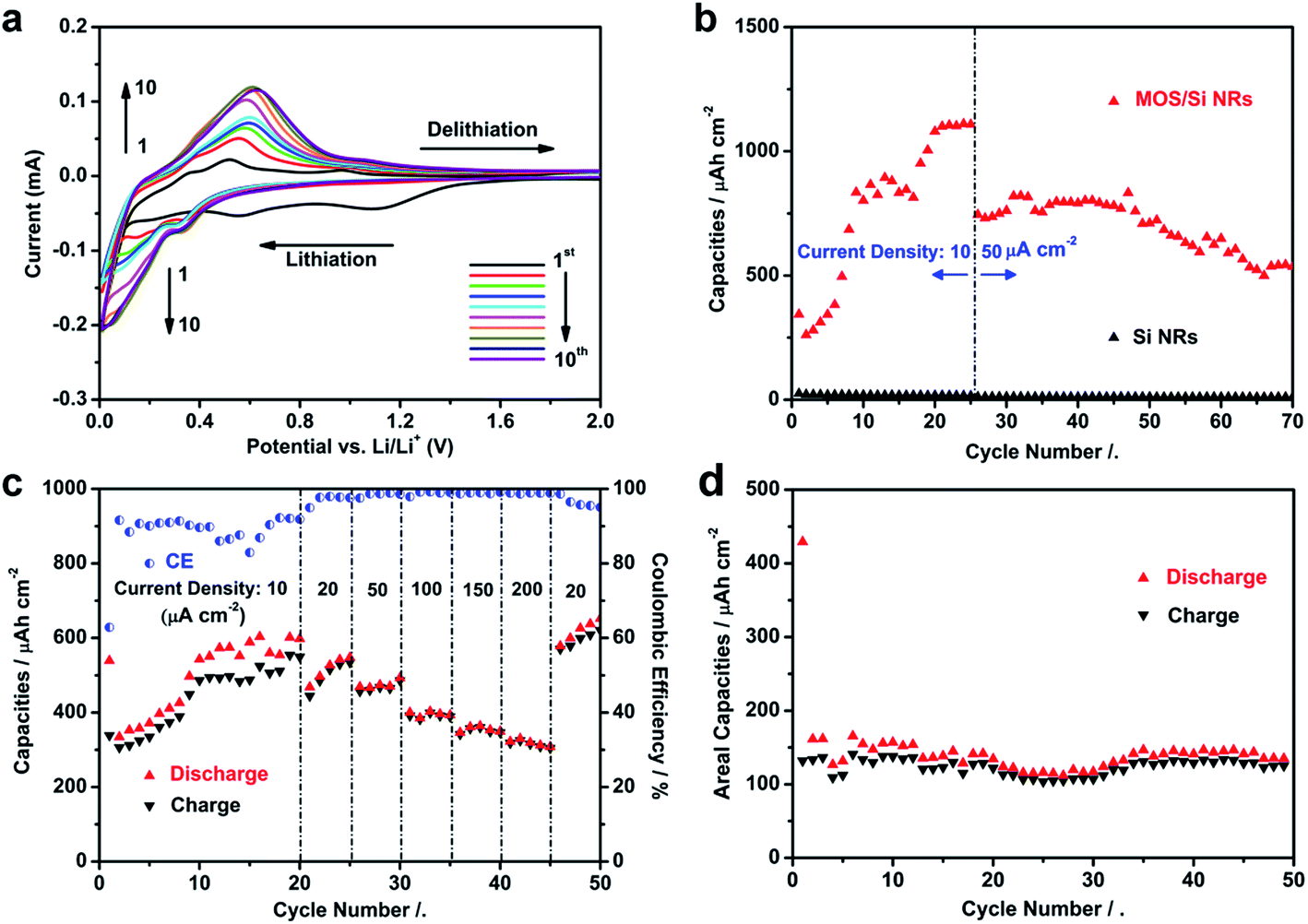 | ||
| Fig. 5 (a) Cyclic voltammograms curves of MOS/Si NRs electrodes in first ten circles within the voltage window between 2.0 V to 0.01 V versus Li/Li+ at a 0.5 mV s−1 sweep rate; (b) discharge capacities of Si NRs and MOS/Si NRs anodes at the current density of 10 and 50 μA cm−2 within the electric potential window from 2.0 V to 0.13 V vs. Li/Li+ till 70th cycles; (c) rate capabilities of the MOS/Si NRs anode at various current densities with its corresponding coulombic efficiency; (d) areal capacities of the ZIF-61/Si NR anodes under the current density of 10 μA cm−2 within the electric potential window from 2.0 V to 0.13 V vs. Li/Li+ till 50th cycles (the MOS/Si NRs samples for the tests were all fabricated at the lower concentration for 12 h). | ||
Conclusion
In conclusion, Si NR surfaces were modified with metal organic segments by the cross-linking of Zn(Ac)2·2H2O, imidazole and 2-methylimidazole with appropriate concentrations and growth time. These kinds of MOS are probably derived from the solution species such as [Zn(C4H6N2)Ac]+, [Zn(C4H6N2)2Ac]+ and [Zn(C3H4N2)(C4H6N2)Ac]+. Due to the cooperation of MOS around Si NRs, resulting in the effective hindering in the formation of SEI film around the Si NR surfaces and restriction of the volume expansion of Si, an up to 1.1 mA h cm−2 capacity was achieved in the composited anode. In addition, the capacity of ∼0.5 mA h cm−2 can be still remained within the high rate cycling. Based on the initial intention in this work, besides the cross-linking of Zn(Ac)2, imidazole and 2-methylimidazole, other kinds of metal sources and imidazolates may also be used to simply modify the surface of nanostructured-Si to achieve improved capacities and longer lifetime in electrodes.Conflicts of interest
There are no conflicts to declare.Acknowledgements
This work is financially supported by the National Basic Research Program of China (2015CB932301), National Natural Science Foundation of China (Grant No. 61675173 and 61505172), Natural Science Foundation of Fujian Province of China (No. 2017H6022), Science and Technology Program of Xiamen City of China (3502Z20161223 and 3502Z20144079).Notes and references
- J.-M. Tarascon and M. Armand, Nature, 2001, 414, 359–367 CrossRef CAS PubMed.
- M. Armand and J.-M. Tarascon, Nature, 2008, 451, 652–657 CrossRef CAS PubMed.
- B. Duun, H. Kamath and J.-M. Tarascon, Science, 2011, 334, 928–935 CrossRef PubMed.
- M. Roberts, P. Johns, J. Owen, D. Brandell, K. Edstrom, G. E. Enany, C. Guery, D. Golodnitsky, M. Lacey, C. Lecoeur, H. Mazor, E. Peled, E. Perre, M. M. Shaijumon, P. Simon and P.-L. Taberna, J. Mater. Chem., 2011, 21, 9876–9890 RSC.
- J. Song, X. Yang, S.-S. Zeng, M.-Z. Cai, L.-T. Zhang, Q.-F. Dong, M.-S. Zheng, S.-T. Wu and Q.-H. Wu, J. Micromech. Microeng., 2009, 19, 045004 CrossRef.
- B. A. Boukamp, G. C. Lesh and R. A. Huggins, J. Electrochem. Soc., 1981, 128, 725–729 CrossRef CAS.
- R. A. Sharma and R. N. Seefurth, J. Electrochem. Soc., 1976, 123, 1763–1768 CrossRef CAS.
- S.-C. Lai, J. Electrochem. Soc., 1976, 123, 1196–1197 CrossRef CAS.
- U. Kasavajjula, C. S. Wang and A. J. Appleby, J. Power Sources, 2007, 163, 1003–1039 CrossRef CAS.
- K. Zhao, W. L. Wang, J. Gregoire, M. Pharr, Z. Suo, J. J. Vlassak and E. Kaxiras, Nano Lett., 2011, 11, 2962–2967 CrossRef CAS PubMed.
- M.-H. Park, M. G. Kim, J. Joo, K. Kim, J. Kim, S. Ahn, Y. Cui and J. Cho, Nano Lett., 2009, 9, 3844–3847 CrossRef CAS PubMed.
- C. K. Chan, R. N. Patel, M. J. O'Connell, B. A. Korgel and Y. Cui, ACS Nano, 2010, 4, 1443–1450 CrossRef CAS PubMed.
- F. Xia, S. B. Kim, H. Cheng, J. M. Lee, T. Song, Y. Huang, J. A. Rogers, U. Paik and W. I. Park, Nano Lett., 2013, 13, 3340–3346 CrossRef CAS PubMed.
- R. Ruffo, S. S. Hong, C. K. Chan, R. A. Huggins and Y. Cui, J. Phys. Chem. C, 2009, 113, 11390–11398 CAS.
- H. Wu, G. Chan, J. W. Choi, I. Ryu, Y. Yao, M. T. McDowell, S. W. Lee, A. Jackson, Y. Yang, L. B. Hu and Y. Cui, Nat. Nanotechnol., 2012, 7, 310–315 CrossRef CAS PubMed.
- N. Liu, H. Wu, M. T. McDowell, Y. Yao, C. Wang and Y. Cui, Nano Lett., 2012, 12, 3315–3321 CrossRef CAS PubMed.
- L.-F. Cui, Y. Yang, C.-M. Hsu and Y. Cui, Nano Lett., 2009, 9, 3370–3374 CrossRef CAS PubMed.
- T. Song, H. Cheng, H. Choi, J.-H. Lee, H. Han, D. H. Lee, D. S. Yoo, M.-S. Kwon, J.-M. Choi, S. G. Doo, H. Chang, J. Xiao, Y. Huang, W. I. Park, Y.-C. Chuang, H. Kim, J. A. Rogers and U. Paik, ACS Nano, 2012, 6, 303–309 CrossRef CAS PubMed.
- W. Wei, G. Wang, S. Yang, X. Feng and K. Müllen, J. Am. Chem. Soc., 2015, 137, 5576–5581 CrossRef CAS PubMed.
- X. Liu, J. Zhang, W. Si, L. Xi, B. Eichler, C. Yan and O. G. Schmidt, ACS Nano, 2015, 9, 1198–1205 CrossRef CAS PubMed.
- J. Deng, H. Ji, C. Yan, J. Zhang, W. Si, S. Baunack, S. Oswald, Y. Mei and O. G. Schmidt, Angew. Chem., Int. Ed., 2013, 52, 2326–2330 CrossRef CAS PubMed.
- G. Zeb, P. Gaskell, Y. N. Kim, G. Jalani, X. Xiao, T. Szkopek and M. Cerruti, RSC Adv., 2016, 6, 45519–45524 RSC.
- F. Zhang, X. Yang, Y. Xie, N. Yi, Y. Huang and Y. Chen, Carbon, 2015, 82, 161–167 CrossRef CAS.
- Y. Sun, L. Fan, W. Li, Y. Pang, J. Yang, C. Wang and Y. Xia, RSC Adv., 2016, 6, 101008–101015 RSC.
- H. Wang, J. Xie, S. Zhang, G. Cao and X. Zhao, RSC Adv., 2016, 6, 69882–69888 RSC.
- D. Ji, Z. Yang, L. Xiong, H. Luo, G. Xiong, Y. Zhu and Y. Wan, RSC Adv., 2017, 7, 4209–4215 RSC.
- Z. Yang, Y. Xia, J. Ji, B. Qiu, K. Zhang and Z. Liu, RSC Adv., 2016, 6, 12107–12113 RSC.
- M. Zhang, T. Zhang, Y. Ma and Y. Chen, Energy Storage Materials, 2016, 4, 1–14 CrossRef.
- C. Li, T. Shi, D. Li, H. Yoshitake and H. Wang, RSC Adv., 2016, 6, 34715–34723 RSC.
- B. Zhao, Y. Jiang, H. Zhang, H. Tao, M. Zhong and Z. Jiao, J. Power Sources, 2009, 189, 462–466 CrossRef CAS.
- Y. Jiang, X. Ling, Z. Jiao, L. Li, Q. Ma, M. Wu, Y. Chu and B. Zhao, Electrochim. Acta, 2015, 153, 246–253 CrossRef CAS.
- B. Zhao, P. Liu, H. Zhuang, Z. Jiao, T. Fang, W. Xu, B. Lu and Y. Jiang, J. Mater. Chem. A, 2013, 1, 367–373 CAS.
- N. Tronganh, Y. Yang, F. Chen, M. Lu, Y. Jiang, Y. Gao, L. Cheng and Z. Jiao, RSC Adv., 2016, 6, 74436–74444 RSC.
- W. Long, B. Fang, A. Ignaszak, Z. Wu, Y. Wang and D. Wilkinson, Chem. Soc. Rev., 2017 10.1039/c6cs00639f.
- B. Fang, M. Kim, J. Kim, S. Lim and J. Yu, J. Mater. Chem., 2010, 20, 10253–10259 RSC.
- J. M. Jeong, B. G. Choi, S. C. Lee, K. G. Lee, S. J. Chang, Y. K. Han, Y. B. Lee, H. U. Lee, S. Kwon, G. Lee, C. S. Lee and Y. S. Huh, Adv. Mater., 2013, 25, 6250 CrossRef CAS PubMed.
- I. Son, J. Park, S. Kwon, S. Park, M. Rümmeli, A. Bachmatiuk, H. Song, J. Ku, J. Choi, J. Choi, S. Doo and H. Chang, Nat. Commun., 2015, 6, 7393 CrossRef CAS PubMed.
- T. Song, H. Cheng, K. Town, H. Park, R. W. Black, S. Lee, W. I. Park, Y. Huang, J. Rogers, L. F. Nazar and U. Paik, Adv. Funct. Mater., 2014, 24, 1458–1464 CrossRef CAS.
- Y. Yu, C. Yue, X. Lin, S. Sun, J. Gu, X. He, C. Zhang, W. Lin, D. Lin, X. Liao, B. Xu, S. Wu, M. Zheng, J. Li and J. Kang, ACS Appl. Mater. Interfaces, 2016, 8, 3992–3999 CAS.
- Y. Yu, C. Yue, S. Sun, W. Lin, H. Su, B. Xu, J. Li, S. Wu, J. Li and J. Kang, ACS Appl. Mater. Interfaces, 2014, 6, 5884–5890 CAS.
- C. Yue, Y. Yu, Z. Wu, X. He, J. Wang, J. Li, C. Li, S. Wu, J. Li and J. Kang, Nanoscale, 2014, 6, 1817–1822 RSC.
- K. Barthelet, J. Marrot, D. Riou and G. Férey, Angew. Chem., Int. Ed., 2002, 41, 281–284 CrossRef CAS PubMed.
- X. Li, F. Cheng, S. Zhang and J. Chen, J. Power Sources, 2006, 160, 542–547 CrossRef CAS.
- K. Saravanan, M. Nagarathinam, P. Balaya and J. J. Vittal, J. Mater. Chem., 2010, 20, 8329–8335 RSC.
- X. Zheng, Y. Li, Y. Xu, Z. Hong and M. Wei, CrystEngComm, 2012, 14, 2112–2116 RSC.
- C. D. Wessells, R. A. Huggins and Y. Cui, Nat. Commun., 2011, 2, 550 CrossRef PubMed.
- Y. Han, P. Qi, X. Feng, S. Li, X. Fu, H. Li, Y. Chen, J. Zhou, X. Li and B. Wang, ACS Appl. Mater. Interfaces, 2015, 7, 2178–2182 CAS.
- N. Liu, Y. Yao, J. Cha, M. McDowell, Y. Han and Y. Cui, Nano Res., 2012, 5, 109–116 CrossRef CAS.
- J. Lippke, B. Brosent, T. von Zons, E. Virmani, S. Lilienthal, T. Preusse, M. Hulsmann, A. M. Schneider, S. Wuttke and P. Behrens, Inorg. Chem., 2017, 56, 748–761 CrossRef CAS PubMed.
- W. Li, F. Lin, X. Li, L. Zhang, W. You and Z. Jiang, J. Coord. Chem., 2013, 66, 2829–2842 CrossRef CAS.
- R. Banerjee, A. Phan, B. Wang, C. Knobler, H. Furukawa, M. O'Keeffe and O. M. Yaghi, Science, 2008, 319, 939–943 CrossRef CAS PubMed.
- L. Ratke and P. W. Voorhees, Growth and Coarsening: Ostwald Ripening in Material Processing, Springer, 2002, pp. 117–118 Search PubMed.
- I. H. Lim, W. Schrader and F. Schuth, Chem. Mater., 2015, 27, 3088–3905 CrossRef CAS.
- P. Y. Moh, P. Cubillas, M. W. Anderson and M. P. Attfield, J. Am. Chem. Soc., 2011, 133, 13304–13307 CrossRef CAS PubMed.
- C. K. Chan, H. Peng, G. Liu, L. K. McIlwrath, X. F. Zhang, R. A. Huggins and Y. Cui, Nat. Nanotechnol., 2008, 3, 31–35 CrossRef CAS PubMed.
Footnote |
| † Electronic supplementary information (ESI) available. See DOI: 10.1039/c7ra10905a |
| This journal is © The Royal Society of Chemistry 2017 |