
 Open Access Article
 This Open Access Article is licensed under a
 Creative Commons Attribution 3.0 Unported Licence
Influence of external electric field on the electronic structure and optical properties of pyrite
Yuqiong Liab,
Jianhua Chen *c and
Cuihua Zhao*b
*c and
Cuihua Zhao*b
aGuangxi Colleges and Universities Key Laboratory of Minerals Engineering, Guangxi University, Nanning 530004, China
bSchool of Resources, Environment and Materials, Guangxi University, Nanning 530004, China. E-mail: xiaocui2000110@163.com
cInnovation Center for Metal Resources Utilization and Environment Protection, Guangxi University, Nanning, China. E-mail: jhchen@gxu.edu.cn
First published on 15th December 2017
Abstract
Pyrite (FeS2) is an attractive photovoltaic material due to its high absorption coefficient and suitable band gap. This work focuses on the effect of external electric field on the electronic band structure and optical properties using density functional theory with Hubbard U correction (DFT+U). Calculations suggest that the application of electric field in x, y and z directions produce similar results both in band structure and optical properties of pyrite. The addition of external electric field has not changed the p-type semiconductivity but band splits significantly and the gap also decreases obviously at high electric field, accompanied with the fracture of the crystal. The variation of dielectric function, absorption coefficient, reflectivity, refractive index, extinction coefficient and conductivity are observed due to the addition of electric field.
1. Introduction
Pyrite, which is the most common sulphide mineral on earth, has received much attention due to its high light absorption coefficient (>10−5 cm−1) for applications as optoelectronic and photovoltaic materials.1–5 It can be made into ultrathin film solar cells due to its high light absorption coefficient. However, its band gap of 0.95 eV is far lower than the theoretical optimal gap of ∼1.3 eV for good photovoltaic materials proposed by Shockley and Queisser.6 Much fundamental research has been carried out aiming to understand the optical properties and electronic structures of pyrite and improve the photovoltaic performance, including doping/alloying with ions (cation ions such as transition metals, anion ions such as oxygen and arsenic elements)5,7–9 varying surface stoichiometry,10 changing the preparation process for pyrite thin films,11–14 etc. However, the external electric effect has not been considered in previous studies.In practice, the addition of external electric field has the advantage of being easy to achieve and control, and is environmentally friendly. The electric field effects on the optical properties of a spherical quantum dot have received great interest for fundamental and application research. Applying an electric field to the material can cause electro-optical effects and change the optical properties. It is found that the optical absorption coefficients and the optical refractive index could be affected by electric field.15 Studies on the nanocomposites of benzyl mercaptan-capped cadmium sulfide (CdS) quantum dots found that electro-photoluminescence exhibits field-induced quenching of photoluminescence in the presence of electric fields, and the magnitude of the photoluminescence quenching monotonically increases with increasing field strength.16 Beside the influences on optical properties of materials, external electric field also affects the adsorption of molecules on catalyst interface.17–19
In order to provide an understanding on the nature of electric field effect on optical properties of pyrite, in this paper, theoretical calculations using density functional theory (DFT) were carried out. The influences of different electric field directions and sizes were considered.
2. Computational method
Pyrite (FeS2) belongs to the space group Th6 − Pa![[3 with combining macron]](https://www.rsc.org/images/entities/char_0033_0304.gif) , with the Fe2+ cations on the corners and the face-centers positions of the cubic cell and the S22− dimers (S1–S2) occupying the anion sites. The unit cell of pyrite contains four Fe atoms and eight S atoms, with formula Fe4S8. Each Fe atom is coordinated to six S atoms creating a distorted octahedron, while each S atom is coordinated to three Fe atoms and one S atom in a tetrahedral configuration (see Fig. 1). External electric filed was applied to x, y and z directions to obtain the structural, electronic and optical properties of pyrite.
, with the Fe2+ cations on the corners and the face-centers positions of the cubic cell and the S22− dimers (S1–S2) occupying the anion sites. The unit cell of pyrite contains four Fe atoms and eight S atoms, with formula Fe4S8. Each Fe atom is coordinated to six S atoms creating a distorted octahedron, while each S atom is coordinated to three Fe atoms and one S atom in a tetrahedral configuration (see Fig. 1). External electric filed was applied to x, y and z directions to obtain the structural, electronic and optical properties of pyrite.
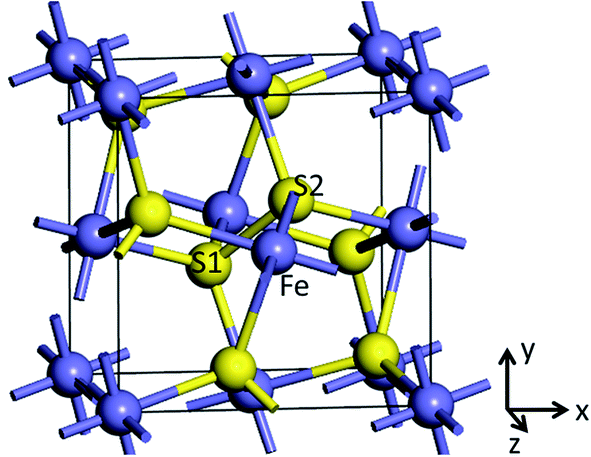 | ||
| Fig. 1 Unit cell of pyrite. x, y, and z indicate the axis direction of the cell. | ||
Structural optimizations and electronic and optical calculations were performed using CASTEP, GGA-PW91.20 The crystal structure was optimized by relaxing both the cell parameters and atomic coordinates. Only the valence electrons (Fe 3d64s2 and S 3s23p4) were considered using ultrasoft pseudopotentials.21 A plane wave cut-off energy of 350 eV was determined by tests and a Monkhorst–Pack22,23 k-point sampling density of 4 × 4 × 4 mesh was used. The self-consistent field (SCF) convergence tolerance was set to 2.0 × 10⁻⁶ eV per atom. The spin calculation was performed during the simulation.
The Hubbard U correction24,25 was adopted for treatment of Fe 3d and specified by tests in this study. Table 1 shows the testing results. It is noted that the band gap of pyrite is only 0.55 eV without the addition of parameter U. With the increase of U value, the band gap of pyrite increases. When 1.2 eV of U value was specified the band gap value of 0.95 eV is the same as the experimental value,26 and also close to the results of Zhang et al.10 and Sun et al.27 using GGA+U with U value of 2.0 eV which gave a band gap of 1.02 eV and 1.03 eV, respectively. Meanwhile, the error (0.56%) of cell parameter (5.3858 Å) in our work calculated at this U level is small compared with the experimental value of 5.4160 Å. The Wyckoff parameter for the position of the S atom (0.3844) is calculated to be very close to the experimental value of 0.3849.28
| Hubbard U value/eV | Band gap/eV | Cell parameter/Å | Wyckoff parameter |
|---|---|---|---|
| 0 | 0.55 | 5.3797 | 0.3829 |
| 1.0 | 0.89 | 5.3846 | 0.3842 |
| 1.2 | 0.95 | 5.3858 | 0.3844 |
| 1.5 | 1.05 | 5.3890 | 0.3847 |
| 2.0 | 1.18 | 5.3940 | 0.3849 |
| Experimental | 0.95 | 5.4160 | 0.3849 |
3. Results and discussion
3.1. Crystal structure
Electric field tests started at 0.05 eV Å−1 e−1 on the condition of 1.2 eV of U value. Fig. 2 shows the cell parameter changes with the increase of electric filed. When electric filed is less than 0.20 eV Å−1 e−1, the cell parameter of pyrite increases slowly with the increase of electric filed in x, y and z directions. In addition, the changes are very similar in the three directions. After that, the differences in lattice parameters progressively become larger. The changes in y and z directions are almost the same, whereas the result in x direction is different from them. It is clear that the increase of cell parameter applying electric field in x direction is faster than in y and z directions. The complete fracture of the crystal is found at 0.23 eV Å−1 e−1 in x direction, while it is occurred at 0.24 eV Å−1 e−1 in y and z directions.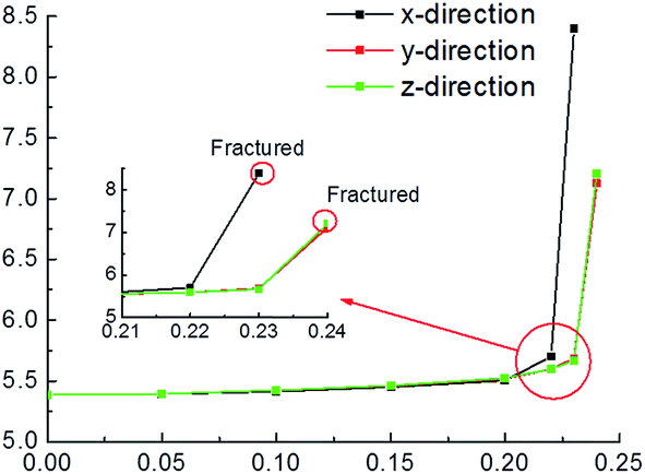 | ||
| Fig. 2 External electric filed effect on the cell parameter at different directions. | ||
The cell parameter expansion is related to the polarization effect produced by the electronic field. Under the polarization effect produced by electric field, the electron cloud of the ions in the lattice distribution is changed, leading to the change of the force on the atom. Consequently, the lattice atomic position varies and the cell parameter changes.
For the atomic structure calculations, we concentrated on the Wyckoff parameter for the position of the S atom. Table 2 shows the cell parameter and sulphur internal coordinate along x, y, and z axes changing with the application of electric field at x, y, and z directions. It is shown that with the increase of electric field applied in x-direction, the Wyckoff parameter decreases slowly but dramatically decreases at x-direction and increases at y-direction once the crystal are fractured, while in y- and z-directions the Wyckoff parameters along x, y, and z axes are decreased gradually.
| Electric field direction | Electric field/eV Å−1 e−1 | Cell parameter/Å | Wyckoff parameter for the position of the S atom | ||
|---|---|---|---|---|---|
| x | y | z | |||
| x-direction | 0 | 5.3858 | 0.3844 | 0.3844 | 0.3844 |
| 0.05 | 5.3921 | 0.3790 | 0.3844 | 0.3843 | |
| 0.1 | 5.4152 | 0.3755 | 0.3835 | 0.3836 | |
| 0.15 | 5.4516 | 0.3736 | 0.3825 | 0.3827 | |
| 0.2 | 5.5034 | 0.3738 | 0.3815 | 0.3812 | |
| 0.23 | 8.4001 | 0.2831 | 0.5558 | 0.3556 | |
| y-direction | 0.05 | 5.3942 | 0.3824 | 0.3800 | 0.3834 |
| 0.1 | 5.4220 | 0.3812 | 0.3756 | 0.3816 | |
| 0.15 | 5.4601 | 0.3796 | 0.3729 | 0.3797 | |
| 0.2 | 5.5217 | 0.3774 | 0.3726 | 0.3772 | |
| 0.25 | 7.1357 | 0.3302 | 0.3743 | 0.3068 | |
| z-direction | 0.05 | 5.3940 | 0.3824 | 0.3842 | 0.3798 |
| 0.1 | 5.4225 | 0.3812 | 0.3828 | 0.3752 | |
| 0.15 | 5.4612 | 0.3800 | 0.3813 | 0.3725 | |
| 0.2 | 5.5255 | 0.3787 | 0.3788 | 0.3719 | |
| 0.24 | 7.2082 | 0.2989 | 0.3320 | 0.3779 | |
The detailed crystal structure changes including bond lengths in pyrite is shown in Table 3. It is clear that at x-direction the S–S and Fe–S bonds lengths increase with the increase of electric field, and the S–S and Fe–S bonds are fractured simultaneous at 0.23 eV Å−1 e−1 of electric field. While the situation at y-direction is completely different that S–S bond is reduced, even at 0.25 eV Å−1 e−1 of electric field it is still not fractured with length of 1.922 Å, in fact the crystal has been fractured at 0.24 eV Å−1 e−1 due to the fracture of Fe–S bond (3.107 Å). For electric field applying at z-direction, both S–S and Fe–S bonds lengths increase with the increase of electric field; however, the S–S bond length increases faster than Fe–S bond length, resulting in the fracture of S–S bond at 0.22 eV Å−1 e−1 while Fe–S bond at 0.24 eV Å−1 e−1 and finally the fracture of the crystal.
| Electric field/eV Å−1 e−1 | x-direction/Å | y-direction/Å | z-direction/Å | |||
|---|---|---|---|---|---|---|
| S–S | Fe–S | S–S | Fe–S | S–S | Fe–S | |
| 0 | 2.154 | 2.250 | 2.154 | 2.250 | 2.154 | 2.250 |
| 0.05 | 2.174 | 2.251 | 2.132 | 2.256 | 2.202 | 2.249 |
| 0.10 | 2.193 | 2.259 | 2.096 | 2.273 | 2.256 | 2.257 |
| 0.15 | 2.209 | 2.275 | 2.050 | 2.296 | 2.302 | 2.270 |
| 0.20 | 2.225 | 2.297 | 1.985 | 2.333 | 2.358 | 2.294 |
| 0.22 | 2.261 | 2.384 | 1.948 | 2.374 | 2.369 | 2.323 |
| 0.23 | 4.656 | 3.341 | 1.913 | 2.520 | 2.437 | 2.352 |
| 0.24 | — | — | 1.927 | 3.107 | 4.125 | 2.943 |
| 0.25 | — | — | 1.922 | 3.114 | — | — |
3.2. Electronic structures
We calculated the electronic properties, including band gap, band structures and density of states (DOS) when electric filed is applied at x, y and z directions. Fig. 3 shows the band gap values as a function of electric field. It is suggested that the band gap of pyrite decreases after an initial slight increase. The increases of band gaps are almost the same in the three directions; however, the decrease of band gap at x direction is faster than at y and z directions. It means that at high electric field the differences of band gaps between x direction and y and z directions are great. In addition, at high electric field the band gap changes are also different between y and z directions. The band gap values in y direction decrease faster than in z direction. | ||
| Fig. 3 Band gap of pyrite applied electric field at different directions. | ||
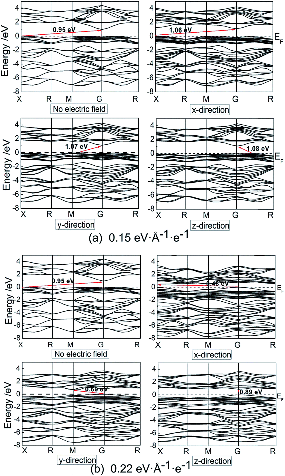
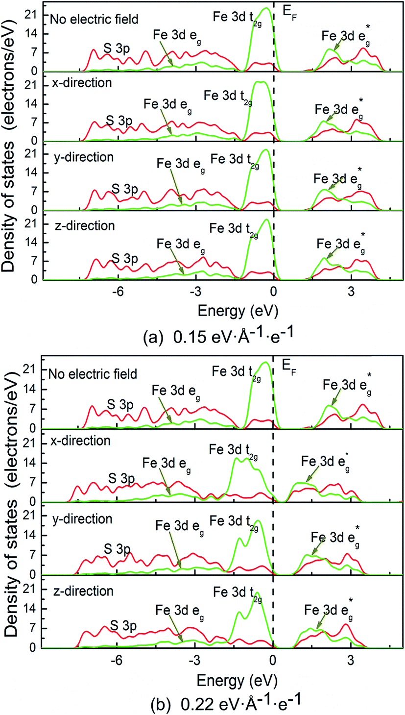
Electronic band structures and density of states (DOS) of pyrite were plotted at electric field of 0.15 and 0.22 eV Å−1 e−1, as shown in Fig. 4 and 5. It is found that when no electric field is applied, pyrite has an indirect p-type band gap from the valence band maximum (VBM) X point to the conduction band minimum (CBD) G(Γ) point. At 0.15 eV Å−1 e−1 (Fig. 4a), regardless of which direction the electric field is applied, the indirect gap p-type is not changed. Moreover, the introduction of electrical field in x direction does not change the positions of VBM and CBD; while electrical field in y and z directions changes the position of VBM.
 | ||
| Fig. 4 Electronic band structures of pyrite at external electric field. | ||
 | ||
| Fig. 5 Density of states (DOS) of pyrite at external electric field. | ||
Higher electrical field has greater influence on the position of VBM and CBD. At 0.22 eV Å−1 e−1 (Fig. 4b), the VBM is changed from X point to G(Γ) point when electric field is applied in either direction; whereas CBD is changed from G(Γ) point to X point, M point and G point in x, y and z directions, respectively. It is suggested applying electric field to z-direction causes the indirect band gap to direct type.
It is noted that no gap state is introduced in the band structure. However, it is found that no matter in which direction the electric field is applied, the energy level is split, especially at high electrical field in the shallow valence band and conduction band. We calculated and plotted the DOS patters shown in Fig. 5a and b. It is clear from the DOS that in valence band, non-bonding Fe 3d t2g state locating at −1.5 to 0 eV splits from on sharp peak to two or three peaks in the three directions, especially splitting significantly at high electric field. In addition, the clear boundary between bonding Fe 3d eg state (−7.5 to 1.5 eV) and non-bonding t2g state (−1.5 to 0 eV) disappears, and the same situation occurs for the two S 3p states locating at these two regions. These suggest that the delocalization of Fe 3d and S 3p electrons in valence band enhances.
3.3. Optical properties
CASTEP can calculate the optical properties of solids due to electronic transitions. In the present study, the frequently used quantity for expressing optical properties: dielectric function, absorption coefficient, and reflectivity, were calculated and the patterns are plotted shown in Fig. 6. Here only the influence of electric filed applied to x-axis is considered due to the results for electric field applied to y- and z-axis are similar to x-axis.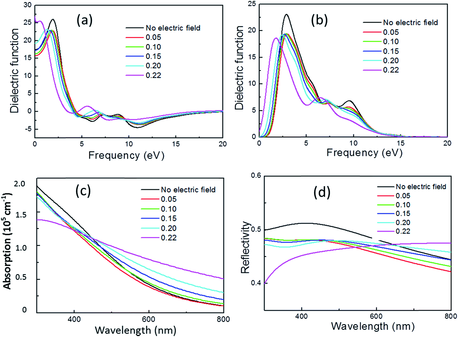 | ||
| Fig. 6 Real part (a) and imaginary part (b) of complex dielectric function, absorption coefficient (c) and reflectivity (d) as a function of electric field. | ||
The complex dielectric function is commonly used to evaluate optical properties and then other properties can be expressed in terms of it. The real and imaginary parts of complex dielectric function are plotted as function of electric field. The Gaussian broadening used for calculating the dielectric function is set to 0.5 eV. The real part of the dielectric function at frequency of 0 eV corresponds to the static dielectric function. It is calculated to be 17.5 without electric filed, compared to 20 for experimental result.29 We calculated the static dielectric function without Hubbard U correction and found a value of 20, consistent with the theoretical calculation result in ref. 29. It is shown that for pyrite with no electric field, there are three dielectric peaks locating at about 3.0, 7.5 and 9.5 eV with the strongest peak occurring at about 3.0 eV. This result is close to the calculation result of Vadkhiya and Ahuja using DFT approach with the full potential augmented plane wave (FP-LAPW) method30 and Antonov et al. using DFT approach with the fully relativistic linear-muffin-tinorbital (RLMTO) method.31 However, the Hubbard U correction may make a shift of the critical points of dielectric function.29
In the presence of external electric field, the static dielectric function decrease at electric field smaller than 0.15 eV Å−1 e−1 but increases after that, especially increases up to about 25 at 0.22 eV Å−1 e−1. For the imaginary part, peak intensity at about 3.0 eV and 9.5 eV significantly decreases and the peak at about 9.5 eV is almost disappeared with the increase of electric field, while the peak intensity at about 7.5 eV slightly increases. In addition, the larger the electric field, the more obvious the whole dielectric function shifts to the low energy direction.
The absorption of visible light across pyrite was investigated in terms of electric field. It is found that the absorption coefficients of pyrite are between 0.25 and 2.0 × 105 cm−1. The application of electric field leads to a decrease of absorption coefficient at wavelength less than 450 nm, but leads to a red shift of absorption edge, and with the increase of electric field the absorption edge red shift increases.
The light reflectivity of pyrite is plotted. The application of electric field results in the decrease of light reflectivity of pyrite in visible light region, even small electric field is applied the change in reflectivity is significant. However, it is found that with the increase of electric field larger than 0.20 eV Å−1 e−1, the light reflectivity increase when wavelength is larger than 650 nm compared with no application of electric field.
4. Conclusion
In conclusion, the application of electric field in x, y and z directions produces similar results both in band structure and optical properties of pyrite. The crystal will be fractured at high electric field, but the fracture of intrinsic Fe–S and S–S bond is different at the three directions with electric field. The p-type semiconductivity of pyrite is not changed but band splits significantly and the gap also decreases obviously at high electric field. With the increase of electric filed, the number of dielectric peaks is changed from 3 to 2. The absorption edge is red shifted but the reflectivity decreases.Conflicts of interest
There are no conflicts to declare.Acknowledgements
The research was supported by the National Natural Science Foundation of China (NSFC. 51764002 and 51574092), the Guangxi Natural Science Foundation (2017GXNSFAA198216), and by the open foundation of Guangxi Colleges and Universities Key Laboratory of Minerals Engineering (GXMP201602-1).References
- A. Ennaoui and H. Tributsch, Sol. Cells, 1984, 13, 197 CrossRef CAS.
- A. Ennaoui, S. Fiechter, C. Pettenkofer, N. Alonso-Vante, K. Buker, M. Bronold, C. Hopfner and H. Tributsch, Sol. Energy Mater. Sol. Cells, 1993, 29, 289 CrossRef CAS.
- S. Nakamura and A. Yamamoto, Sol. Energy Mater. Sol. Cells, 2001, 65, 79 CrossRef CAS.
- P. P. Altermatt, T. Kiesewetter, K. Ellmer and H. Tributsch, Sol. Energy Mater. Sol. Cells, 2002, 71, 181 CrossRef CAS.
- S. Khalid, M. A. Malik, D. J. Lewis, P. Kevin, E. Ahmed, Y. Khan and P. O'Brien, J. Mater. Chem. C, 2015, 3, 12068 RSC.
- W. Shockley and H. J. Queisser, J. Appl. Phys., 1961, 32, 510 CrossRef CAS.
- B. Mao, Q. F. Dong, Z. G. Xiao, C. L. Exstrom, S. A. Darveau, T. E. Webber, B. D. Lund, H. Huang, Z. H. Kang and J. S. Huang, J. Mater. Chem. C, 2013, 1, 12060 RSC.
- J. Hu, Y. N. Zhang, M. Law and R. Wu, J. Am. Chem. Soc., 2012, 32, 13216 CrossRef PubMed.
- R. S. Sun, M. K. Y. Chan, S. Y. Kang and G. Ceder, Phys. Rev. B: Condens. Matter Mater. Phys., 2011, 84, 035212 CrossRef.
- Y. N. Zhang, J. Hu, M. Law and R. Q. Wu, Phys. Rev. B: Condens. Matter Mater. Phys., 2012, 85, 085314 CrossRef.
- C. Wadia, Y. Wu, S. Gul, S. K. Volkman, J. Guo and A. P. livisatos, Chem. Mater., 2009, 21, 2568 CrossRef CAS.
- Y. Bi, Y. Yuan, C. L. Exstrom, S. A. Darveau and J. Huang, Nano Lett., 2011, 11, 4953 CrossRef CAS PubMed.
- L. Zhu, J. R. Beauardson and Q. M. Yu, Nanoscale, 2014, 6, 1029 RSC.
- D. Y. Wang, Y. T. Jiang, C. C. Lin, S. S. Li, Y. T. Wang, C. C. Chen and C. W. Chen, Adv. Mater., 2012, 24, 3415 CrossRef CAS PubMed.
- W. F. Xie, Phys. B, 2010, 405, 3436 CrossRef CAS.
- M. S. Mehata, M. Majumder, B. Mallik and N. Ohta, J. Phys. Chem. C, 2010, 114, 15594 CAS.
- F. Tielens, J. Andrés, T. D. Chau, T. V. Bocarmé, N. Kruse and P. Geerlings, Chem. Phys. Lett., 2006, 421, 433 CrossRef CAS.
- B. T. Visart, T. D. Chau, F. Tielens, J. Andrés, P. Gaspard, R. L. Wang, H. J. Kreuzer and N. Kruse, J. Chem. Phys., 2006, 125, 153 Search PubMed.
- F. Tielens, L. Gracia, V. Polo and J. Andrés, J. Phys. Chem. A, 2007, 111, 13255 CrossRef CAS PubMed.
- J. P. Perdew, J. A. Chevary, S. H. Vosko, K. A. Jackson, M. R. Pederson, D. J. Singh and C. Fiolhais, Phys. Rev. B: Condens. Matter Mater. Phys., 1992, 46, 6671 CrossRef CAS.
- D. Vanderbilt, Phys. Rev. B: Condens. Matter Mater. Phys., 1990, 40, 7892 CrossRef.
- H. J. Monkhorst and J. D. Pack, Phys. Rev. B: Solid State, 1976, 13, 5188 CrossRef.
- J. D. Pack and H. J. Monkhorst, Phys. Rev. B: Solid State, 1977, 16, 1748 CrossRef.
- V. I. Anisimov, J. Zaanen and O. K. Andersen, Phys. Rev. B: Condens. Matter Mater. Phys., 1991, 44, 943 CrossRef CAS.
- V. I. Anisimovy, F. Aryasetiawanz and A. I. Lichtenstein, J. Phys.: Condens. Matter, 1997, 9, 767 CrossRef.
- A. Schlegel and P. Wachter, J. Phys. C: Solid State Phys., 1976, 9, 3363 CrossRef CAS.
- R. S. Sun, M. K. Y. Chan and G. Ceder, Phys. Rev. B: Condens. Matter Mater. Phys., 2011, 83, 235311 CrossRef.
- M. Rieder, J. C. Crelling, O. Šustai, M. Drábek, Z. Weiss and M. Klementová, Int. J. Coal Geol., 2007, 71, 115 CrossRef CAS.
- S. G. Choi, J. Hu, L. S. Abdallah, M. Limpinsel, Y. N. Zhang, S. Zollner, R. Q. Wu and M. Law, Phys. Rev. B: Condens. Matter Mater. Phys., 2012, 86, 115207 CrossRef.
- L. Vadkhiya and B. L. Ahuja, J. Alloys Compd., 2011, 509, 3042 CrossRef CAS.
- V. N. Antonov, L. P. Germash, A. P. Shpak and A. N. Yaresko, Phys. Status Solidi B, 2009, 246, 411 CrossRef CAS.
| This journal is © The Royal Society of Chemistry 2017 |