
 Open Access Article
 This Open Access Article is licensed under a Creative Commons Attribution-Non Commercial 3.0 Unported Licence
One-pot synthesis of MoS2/WS2 ultrathin nanoflakes with vertically aligned structure on indium tin oxide as a photocathode for enhanced photo-assistant electrochemical hydrogen evolution reaction†
Xinxin Jiang,
Baoliang Sun,
Ye Song,
Meiling Dou,
Jing Ji* and
Feng Wang *
*
State Key Laboratory of Chemical Resource Engineering, Beijing Key Laboratory of Electrochemical Process and Technology for Materials, Beijing University of Chemical Technology, Beijing 100029, China. E-mail: jijing@mail.buct.edu.cn; wangf@mail.buct.edu.cn
First published on 23rd October 2017
Abstract
A hierarchical structure composed of vertically aligned ultrathin two dimensional (2D) MoS2/WS2 nanosheets is fabricated through a facile one-pot hydrothermal reaction. Scanning electron microscope (SEM), transmission electron microscope (TEM) and photoluminescence (PL) indicate that the MoS2/WS2 hybrid shows ultrathin nanoflakes with a thickness of 2–10 nm, and the as prepared heterostructure markedly enhances the separation of electro–hole pairs. Benefiting from the integrated W-doped MoS2, the vertically aligned nanostructure exhibits a moderate degree of disorder and increased active surface area. Electrochemical measurements (cyclic voltammetry (CV), linear sweep voltammetry (LSC) and electrochemical impedance spectroscope (EIS) under light illumination or in dark) indicated that the MoS2/WS2 hybrid (especially the hybrid with Mo![[thin space (1/6-em)]](https://www.rsc.org/images/entities/char_2009.gif) :W of 1/1) exhibits much better photo-and electrochemical performance than its counterpart of pure MoS2 or WS2, which made it a promising photocathode for electrocatalytic hydrogen evolution reaction (HER) by photo-assistance.
:W of 1/1) exhibits much better photo-and electrochemical performance than its counterpart of pure MoS2 or WS2, which made it a promising photocathode for electrocatalytic hydrogen evolution reaction (HER) by photo-assistance.
1. Introduction
Investigation of photoelectrocatalytic activities in transition metal dichalcogenides (TMDs) has revealed a new category of photonic nanomaterials with potential applications in hydrogen evolution reaction (HER).1–16 These materials are characterized by a unique 2 dimensional (2D) structure of trigonal-prismatic metal centres with weak interlayer S–S bonding. Among the TMDs, WS2 and MoS2 have an analogous structure and share similar physical and chemical properties. Both are the most interesting layered materials for HER because their hydrogen binding energy is close to that of Pt-group metals,17 and are considered as an alternative electrocatalyst to Pt-group metals towards the HER.18–22 In addition, their graphene-like structure possesses direct band gaps corresponding well to visible-to-near-IR photon energies,23 therefore, are much suitable in many optoelectronic applications.24–26However, MoS2 or WS2 alone has negligible photocatalytic activity probably due to the fact that MoS2 or WS2 has a relative narrow band gap, and thus is liable to cause recombination of photoinduced electron–hole. Up to now, most of MoS2 or WS2 based photoelectrocatalyst reported for HER applications concerned with traditional photocatalytic materials (e.g., MoS2/CdS, WS2/CdS,27 MoS2/Cu2O,28 MoS2/graphene/CdS,29 MoS2/TiO230 etc.).
Theoretical calculations have shown that MoS2/WS2 heterostructures present an ideal energy band alignment of type-II semiconductors which is in favor of the separation of photoinduced electron–hole pairs.31,32 And some investigations have quantitatively analysed and probed the model heterostructure MoS2/WS2 concerning with the 2D spatial distributions of the built in potential and the related electronic structure.33,34 Therefore, the cocatalyst of coupling of MoS2 with WS2 has the potential in the applications of photocatalysis.
On the other hand, the photo-and electrocatalytic activities can be improved by ways of tuning the morphologies of TMDs. Since previous experiments35–37 and density function theory studies38 have shown that the edges of MoS2 were identified as active sites for the HER, and both WS2 and MoS2 show morphology-dependent photo- and electrocatalytic activities,39–43 a large body of work has been directed at design and control of the morphologies and microstructures. Specifically, the investigations focused on controllable growth of MoS2 or WS2 nanostructures, especially as nanoparticles and mono-or- fewer layers that maximally expose active edge sites to the reactants, and optimization of the number of active sites by elemental doping TMDs.44–47
From the view point of electrocatalytic kinetics, vertically aligned 2D nanostructures on the conductive substrate is an ideal morphology for enhancing the photoelectrocatalytic activity due to their abundant active sites,48 large specific surface and easy electron transportation. Many different synthesis methods for the preparation of vertically aligned TMD-based 2D structured materials have been explored. However, the preparation of vertically aligned 2D nanosheets usually grows on the carbon based49,50 or porous substrate51 through multi-step synthetic processes, which find an application only in electrocatalysis for HER. In addition, most photo or electrocatalysts are prepared in form of powder assemblies, and require binder to prepare the electrodes. The related photo- or eletrocatalytic reaction is conducted either under open-circuit conditions (the electron and hole transport at the same electrode) using power suspensions or catalyst fixed on a support (especially for the electrocatalyst for HER, which is generally used as the cathode), or alternatively in a photo-electrochemical setting in which bias potential is applied to enhance the photocurrent.
To make use of the integration of electro- and photocatalytic activities as a superior photoelectrocatalyst for PEC cells, vertically aligned nanostructure of ultrathin 2D MoS2/WS2 nanosheets which is directly grown on transparent indium tin oxide (ITO) substrates is very critical, since they are compatible with the direct photocatalytic applications. This hybrid structure not only favors light harvesting and adsorption, but also is beneficial to fast electron transportation, ion diffusion and sufficient electrochemical reaction of individual nanostructures due to enriched active sites and binder free combination.
In this work, hierarchical structures composed of vertically aligned ultrathin 2D MoS2/WS2 nanosheets were fabricated through a facile one-pot hydrothermal reaction. By this approach, the whole scale of vertically grown ultrathin MoS2/WS2 sheets was fabricated directly on ITO substrate. Herein, the hybrid nanosheets of MoS2/WS2 supplied numbers of active sites with proper defects since the elements of Mo and W doped with each other. More meaningful, favorable band alignment, as well as intimate p–n heterojunction between MoS2 and WS2, provides an effective carrier separation in this composite based photoelectric device. Consequently, the as-synthesized composites of MoS2/WS2 nanosheets shows better visible light activities than that of either pure WS2 or MoS2 nanostructures and shows great potential for integration of electro- and photocatalysis as a superior photoelectrocatalyst for PEC cells.
Up to now, the investigations on MoS2/WS2 composites mainly focused on the electronic structure of the model heterostructure, and little attention has been given to the influence of the as prepared nanostructures on their photo-and electrocatalytic activities. Among the few literatures related to the photoelectrocatalysis of RHE for MoS2/WS2 composites (Table 1), the photoelectrocatalytic activity is far from satisfactory, and still needs to be improved. The rational use of the MoS2/WS2 cathode provided a new avenue toward achieving an enhanced electrocatalytic activity by photo-assistance.
| Photoelectrode | Light intensity (mW cm−2) | Electrolyte | Potential at −10 mA current density (vs. RHE) | Ref. (year) |
|---|---|---|---|---|
| SnO2@MoS2/FTO | 150 W xenon lamp (400 nm cutoff filter, ∼300 mW cm−2) | 0.10 M Na2SO4 electrolyte solution | −0.73 V | 61 (2017) |
| MoS2@Cu2O/FTO | A 350 W Xe arc lamp | Na2SO4 (0.1 mol L−1, pH = 7) aqueous solution. | −0.47 mA at −1.5V vs. SCE | 62 (2014) |
| Vertical WS2 or MoS2/SiO2 | 0.50 M H2SO4 | −0.34 or −0.41 V | 63 (2016) | |
| 1T@2H–MoS2/FTO | Visible light excitation | Na2SO4 (0.5 mol L−1) | −5 mA at −1.0 V vs. Ag/AgCl | 64 (2016) |
| Vertical aligned WS2/MoS2/ITO | A 300W Xe arc lamp (CEL-HXF300) equipped with an ultraviolet cutoff filter (λ > 420 nm) ∼100 mW cm−2 | 0.50 M H2SO4 | −0.37 V | This work |
| WS2/MoS2/Au | 100 mW cm−2 using a 300 W Xe lamp as source with a cut-off filter (>420 nm, newport) | 0.5 M H2SO4 | −0.24 V | 65 (2016) |
| WS2/MoS2 composites of nanosheets and quantum dots/GCE | 0.50 M H2SO4 | −0.26 V | 66 (2015) | |
| Vertical aligned WS2/MoS2/Ti | 0.50 M H2SO4 | −0.21 V | This work (ESI Fig. S6) |
2. Experimental section
2.1. Materials
Sulfuric acid was purchased from Sinopharm Chemical Reagent Co., Ltd. Sodium molybdate dehydrate, sodium tungstate dehydrate and thioacetamide was obtained from J&K. Indium tin oxide (ITO) coated glass was purchased from China South Glass. Deionized water (resistivity > 18.4 MΩ cm−1) was prepared using a pure water system (TTL-6B). All chemical reagents were used without further purification.2.2. Preparation of MoS2/WS2 vertical mesh-shaped structure
A simple hydrothermal method was preferred to prepare the vertical aligned MoS2/WS2 ultrathin sheets on the ITO substrate. The ITO substrate was ultrasonically cleaned in acetone, ethanol and deionized (DI) water for 15 min each, respectively, prior to use. In a typical reaction, a 2 × 4 cm2 area of the ITO substrate was placed vertically at the bottom of the Teflon-lined stainless-autoclave (25 ml) and immersed in a solution composing of 0.0086 mmol of (NH4)6Mo7O24·4H2O, 0.06 mmol of Na2WO4·2H2O and 0.4 mmol of L-cystine. And then, the autoclave was sealed and thermally treated at 220 °C for 20 hours. The as-prepared sample of vertically aligned MoS2/WS2 hybrid nanosheets (labelled MoS2/WS2) was then removed from the solution, washed thoroughly with ethanol and distilled water, and dried naturally. In control experiments, the vertically aligned pristine MoS2 and WS2 structures on the ITO substrate were prepared by the similar hydrothermal method, respectively, with that of MoS2/WS2 nanosheets, except that the ITO is immersed in a solution composing of 0.0172 mmol (NH4)6Mo7O24·4H2O, or 0.12 mmol Na2WO4·2H2O and 0.4 mmol L-cystine. In control experiments, the precursors of MoS2 and WS2 are stoichiometrically fed into the reaction system in mole ratio of 2:1, 1:1, and 1:2 for Mo/W, which is designated as the mole ratio of Mo and W (2:1), (1/1) and (1/2), respectively. It is notably that the concentration of (NH4)6Mo7O24·4H2O remains constant regardless of the mole ratio of Mo/W.
2.3. Characterization
Scanning electron microscopy (SEM) investigation was conducted by a JEOL-6701F field emission scanning electron microscope which is operated at a scanning current of 10 μA and an accelerating voltage of 5 kV. High resolution transmission electron microscopy (HRTEM) is performed by a JEOL JSM-3010 instrument operated at 200 kV. High-angle annular dark-field scanning transmission electron microscopy (HAADF-STEM) and corresponding energy dispersive spectroscopy (EDS) mapping analysis were carried out on a JEOL JEM-2010F STEM. The crystal phases of the samples were collected on an X-ray diffractometer with Cu–K radiation at a scan rate of 5° min−1 (Rigaku D/max-2500B2+/PCX). X-ray photoelectron spectroscopy (XPS) was performed on the as-synthesized samples using a ESCALAB 250 XPS system with an Al Kα source (Thermo Fisher Scientific USA). UV-visible diffuse reflectance spectra were recorded using a UV-visible spectrophotometer with an integrating sphere (Shimadzu UV2450, Japan). Photoluminescence measurements (PL) were carried out on a Hitachi F-4500 FL spectrophotometer at an excitation wavelength of 400 nm.2.4. Electrochemical measurements
Electrochemical experiments were performed in a three-electrode cell in which a Pt plate and calomel were used as the counter and reference electrodes, respectively, and the as prepared samples were employed as the working electrode with an area of 0.16 cm2. All the samples were analysed in 0.50 M H2SO4 solution (pH = 0.48). A 300W Xe arc lamp (CEL-HXF300) equipped with an ultraviolet cutoff filter (λ > 420 nm) was utilized as the visible light source with 150 mW cm−2 incident light intensity. Linear sweep voltammetry (LSV) with scan rate of 10 mV s−1 was conducted by an electrochemical workstation (CHI660E, Chenhua, China). All the potentials were transformed into the reversible hydrogen electrode (RHE) according to the Nernst equation:E(vs. RHE) = E(vs. SCE) + 0.0591 pH + E0SCE. E0SCE = 0.245 V at 25 °C. EIS measurements were performed at an overpotential of −0.559 V vs. RHE over frequency range from 10−1 to 105 Hz. Electrochemical capacitance measurements were conducted by cyclic voltammetry (CV) for two cycles between 0.1 and 0.2 V vs. RHE with scanning rates of 60, 80, 100, 120 and 150 mV s−1.
2.5. Photocatalytic activity measurement for HER
The photocatalytic H2 production reactions of photocatalysts were carried out under open-circuit conditions (electron and hole transfer occur from the same electrode) using MoS2/WS2 layers fixed on an ITO support (8 cm2). Specifically, the photocatalytic H2 evolution is conducted in an outer irradiation-type photoreactor (Pyrexglass) connected to a closed gas-circulation system. The catalyst samples were put into 20 ml of aqueous solution containing 0.50 M H2SO4 solution. The catalysts were irradiated with a 300 W Xe arc lamp (CEL-HXF300). The photocatalytic H2 evolution rate was analyzed with an online gas chromatograph (GC-7920, TCD detector).3. Results and discussion
3.1. Structure characterization
:W ratios display similar morphologies (Fig. S1†). More details of the morphology and microstructure of the MoS2/WS2 hybrid nanosheets can be obtained from their TEM and HRTEM surveys shown in Fig. 2a–c. As revealed in Fig. 2b, a single MoS2/WS2 hybrid nanosheet consists of 2 to 10 layers, less than 10 nm, and each interlayer distance is characterized by ∼0.62 nm (002). The lattice-resolved HRTEM image shown in Fig. 2c, enclosed by red boxes, and the corresponding FFT pattern indicate the highly crystalline characteristics and undoubtedly attributes to the hexagonal characteristics of the 2H–MoS2 (upper right). In addition, the HRTEM image of the MoS2/WS2 hybrid nanosheets shown in Fig. 2c, enclosed by dark blue boxes, show some trigonal lattice area (octahedral coordination) of the 1T phase besides the common honey-comb lattice area of the trigonal prismatic coordination in the 2H phase. Nevertheless, the FFT of Fig. 2c (lower right) does not reveals the perfect hexagonal packing usually observed for 2H structure due to the overlap with the 1T structure. Furthermore, Raman spectra (Fig. S2†) show a set of characteristic peaks for MoS2 nanosheets at 375 cm−1, 403 cm−1 and 445 cm−1 arising from the E12g, A1g and longitudinal acoustic phonon modes,52,53 respectively, which corresponds to the presence of the 2H phase. The peaks at 220 cm−1 is ascribed to the 1T–MoS2 phase, suggesting the existence of 1T phase ingredient embedded in the 2H–MoS2 host.54 1T–MoS2 nanosheets show higher HER catalytic activity than 2H–MoS2 (ref. 12, 54 and 55) due to its metallic characteristics.56 The fringe spacings of 0.27, 0.227, and 0.247 nm correspond to the (100), (103) and (102) planes of MoS2, respectively.
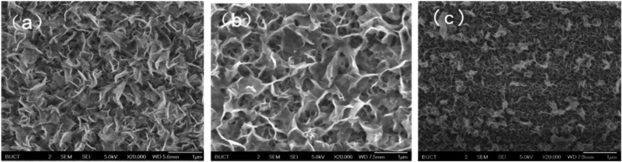 | ||
| Fig. 1 SEM images of (a) WS2, (b) MoS2 and (c) MoS2/WS2 hybrid nanosheets. The calculated mole ratio of Mo:W is 1:1. | ||
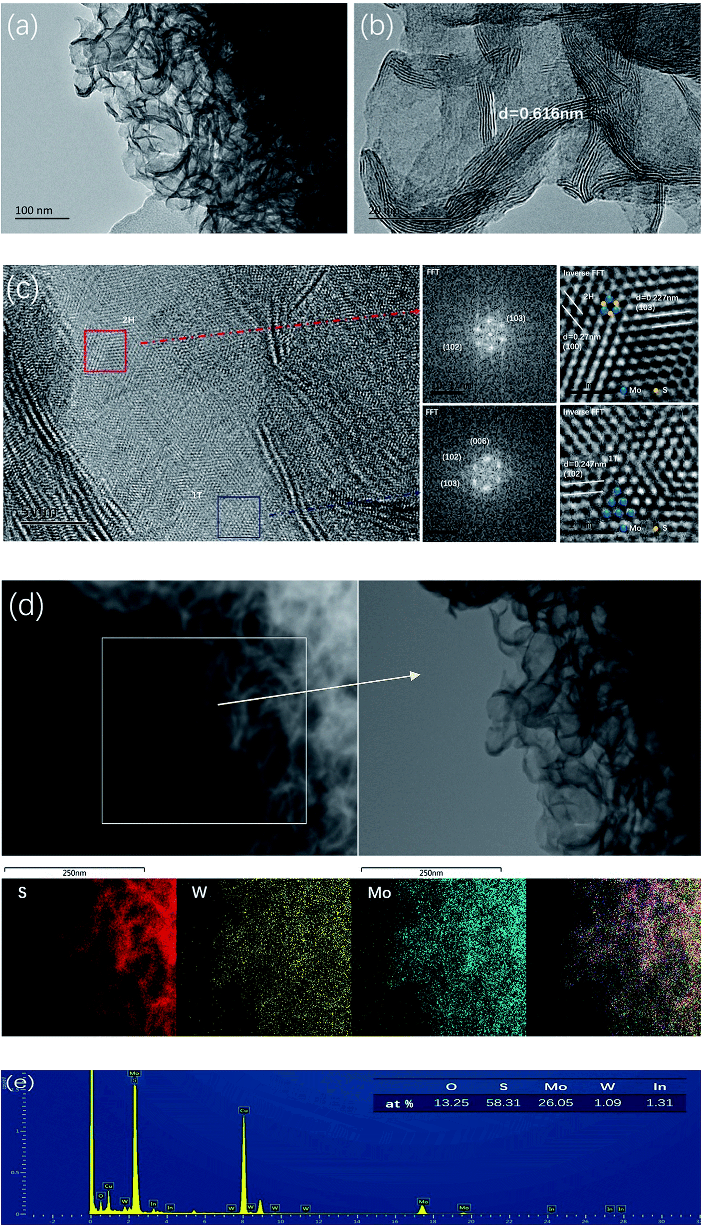 | ||
| Fig. 2 (a) TEM images of MoS2/WS2, (b) HRTEM images, (c) HRTEM image of MoS2/WS2 with its corresponding Fast Fourier Transform (FFT), highlighting the random orientation of individual building blocks (evidenced by both the lattice fringes and the FFT ring pattern), (d) elemental mapping and (e) EDS spectrum of vertical aligned MoS2/WS2 structure. The calculated mole ratio of Mo:W is 1:1. | ||
The formation of 1T–MoS2 is due to the intercalation of ammonia-ions, thus leading to the release of free 1T-MoS2 nanosheets.57 Nevertheless, the precursor of W source of Na2WO4·2H2O is only beneficial to the formation of 2H structure58
Furthermore, we carried out elemental mapping and energy-dispersive X-ray spectroscopy (EDS) under scanning transmission electron microscopy (STEM) to probe the composition and spatial distribution of the constituent elements. Fig. 2d and e showed the intimate contact between WS2 and MoS2 by showing a perfect spatial correspondence and homogeneous S element distribution. More meaningful, the co-existence of the W and Mo element are both uniformly distributed with each other. The energy-dispersive spectrum (EDS) (Fig. 2e) of the hybrid confirms the coexistence of Mo, W and S, and the atomic ratio of S:Mo:W is 58.3:26.1:1.1, respectively. A relative small ratio of W indicates that the element of W doped MoS2, and WS2 is successfully implanted in the MoS2 nanosheet matrix. However, the small ratio of W determined by EDS in the hybrid is obviously not consistent with the stoichiometric feeding ratio of 1/1. This is because Mo4+ and W4+ have difference in affinity to sulphur59 The equilibrium constant of Mo-sulfidation is two orders of magnitude higher than that of W-sulfidation.60,61 Therefore, the constituent proportion of MoS2 is much higher than that of WS2 in the composite.
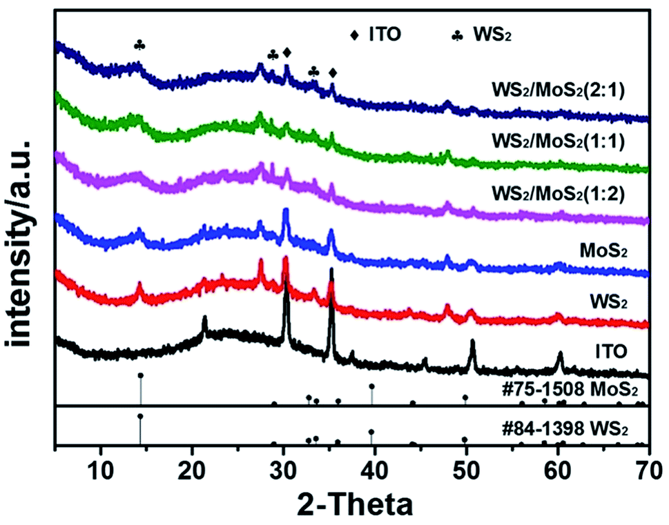 | ||
| Fig. 3 XRD patterns of the as prepared samples. | ||
The as-prepared MoS2/WS2 samples were further analyzed with XPS analysis (Fig. 4). The binding energies for each element are used to identify the individual elements due to their distinct values. In Fig. 4a, the XPS survey spectrum that Mo, W and S elements coexist in the surface elemental composition. Fig. 4b–d revealed a series of high-resolution XPS spectra of W 4f, Mo 3d, and S 2p. As presented in Fig. 4d, the S 2p peak splits into two peaks at 162.1 eV and 163.3 eV, which is corresponding to S 2p3/2 and S 2p1/2, respectively. Two peaks of Mo 3d3/2 at 232.9 eV and Mo 3d5/2 at 229.7 eV are typical characteristics of Mo 3d, and the other two peaks observed at 231.6 and 228.1 eV are ascribed to Mo 3d3/2 (1T) and Mo 3d5/2 (1T), respectively (Fig. 4c).
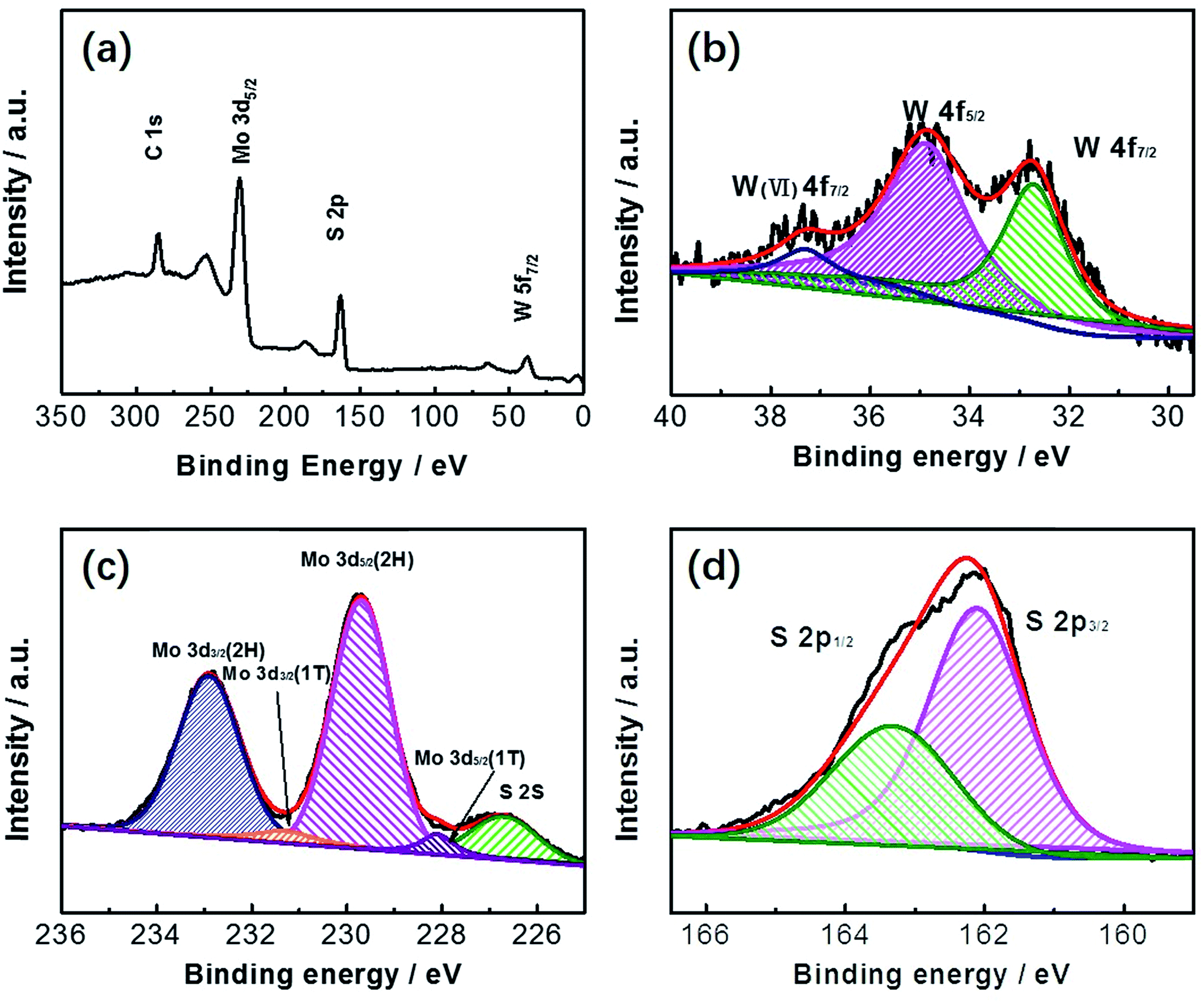 | ||
| Fig. 4 (a) XPS spectrum of the MoS2/WS2 nanosheets, (b) high resolution XPS spectrum of Mo 3d, (c) high resolution XPS spectrum of W 3d, and (d) high resolution XPS spectrum of S 2p. The calculated mole ratio of Mo:W is 1:1. | ||
Two main peaks of W4+ in WS2 are at the binding energies of 32.7 and 34.9 eV, which is the semiconducting prismatic 2H form.62,63 Upon further scrutiny, W6+ was observed are at 37.3 eV, which are due to the presence of WO3.64
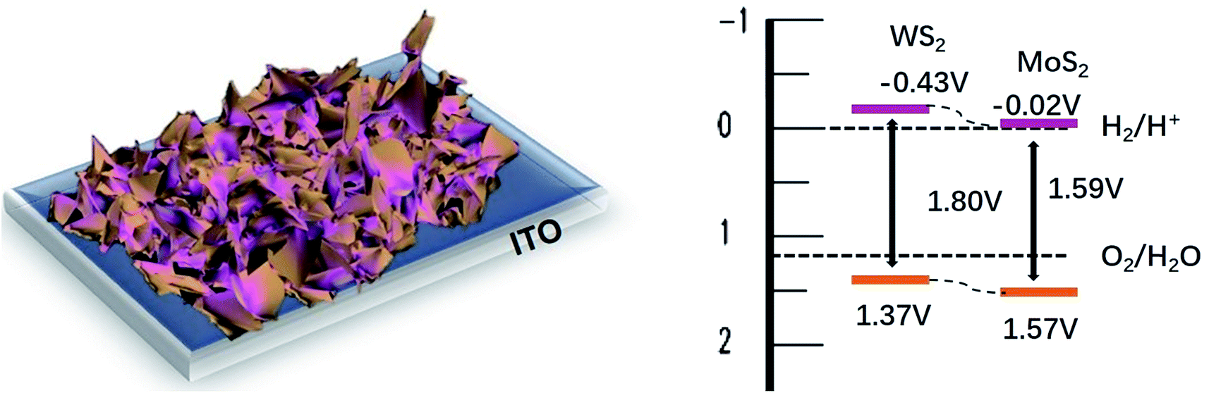
:1 exhibits the strongest adsorption. In addition, the resulting Eg values for WS2, MoS2 and MoS2/WS2(1:1) are 1.59, 1.80 and 1.67 eV, (Fig. S3†) respectively. In this context, both WS2 and MoS2 exhibit a small increase in the band gap, not well consistent with the theoretical bandgap of fewer layers WS2 or MoS2 (∼1.3 eV). The increase in the band gap is properly attributed to the effect of the Eg of In2S3 (∼2.4 eV) derived of ITO under hydrothermal condition (ESI Fig. S4†).
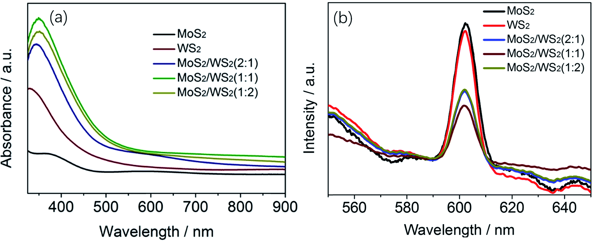 | ||
| Fig. 5 (a) UV-visible absorption spectra of MoS2/WS2(1/1), (b) PL spectra of MoS2/WS2 nanosheets with different stoichiometric mole ratio of Mo:W. | ||
The PL spectra of MoS2 and MoS2/WS2 were measured at an excitation wavelength of 400 nm to assess the separation efficiency of photogenerated electron–hole pairs. According to the PL spectra shown in Fig. 5b, the PL intensity of the MoS2/WS2 heterostructure is much weaker than that of MoS2 or WS2, suggesting reduced recombination of photogenerated charge carriers under illumination. Apparently, the MoS2/WS2 heterostructure with mole ration of 1:1 shows the lowest PL intensity among all of the samples. With the reduced photogenerated charge carrier recombination and thus quick photogenerated charge carrier transportation and the interaction of the photoinduced electrons with H+ in water occurs directly, the as-prepared composite is anticipated to enhance the photocatalytic activity for HER.
To confirm the enhanced separation efficiency of photogenerated charge carriers, we measured the transient photocurrent (chronoamperometric) of the samples at bias of 0.372 V vs. RHE (Fig. 6). All of the samples exhibit good reproducibility of the photocurrent, and the intensity of MoS2/WS2 is much stronger than that of pristine MoS2 or WS2. The strongest photocurrent is obtained from the sample of MoS2/WS2 of 1:1. A higher photocurrent response of the composite suggests that heterostructures do has a higher separation efficiency of photogenerated electrons and holes.65
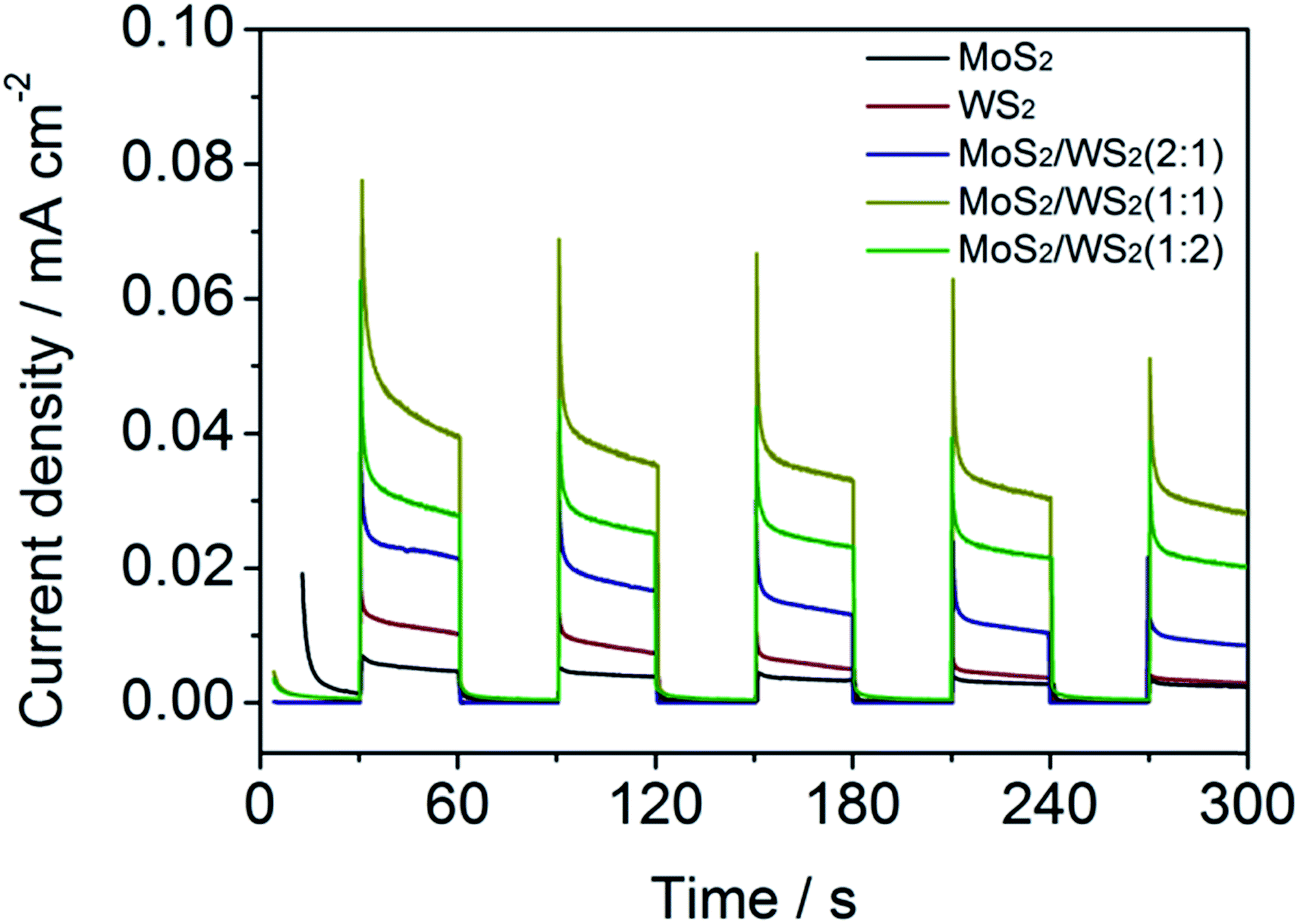 | ||
| Fig. 6 On-off J–t curves of MoS2/WS2 vertically aligned structure of nanosheets prepared with different ratio of Mo to W precursor concentration at bias of 0.372 V vs. RHE in 0.5 mol L−1 H2SO4. | ||
Additionally, operational stability is also an important criterion for a HER catalyst. To assess the stability of MoS2/WS2 for HER, a current density vs. time (I–t) curve was recorded over a longer reaction time (ESI Fig. S5†) at 0.372 V (vs. RHE). As shown in Fig. S5,† MoS2/WS2 (Mo/W = 1:1) electrode showed a photocurrent of ∼0.04 mA in the initial stage of photoirradiation, then decreased to 0.03 mA gradually and maintained the constant photocurrent for more than 7000 s.
:W, were investigated in dark or under light illumination (Fig. 7a). As shown in Fig. 7a, a standalone cathode of MoS2 or WS2 does not show noticeable cathodic current, whether in dark or under illumination condition. As expected, the cathodic polarization curves recorded for the vertically aligned MoS2/WS2 nanostructures exhibited a comparatively obvious photocurrent in comparison with that of standalone cathode of MoS2 or WS2, and shows greater current under light illumination than in the dark. In addition, the cathodic currents for all MoS2/WS2 samples are greater than the sum of the cathodic currents of pristine MoS2 and WS2, implying that the combination of MoS2 and WS2 in hybrid structures is synergistic rather than additive. The nano-structured MoS2/WS2 electrode (Mo/W ratio of 1/1) displays the highest current density among all the tested electrodes. Fig. 7b shows the differences in photocurrent density of the catalysts at the potential of −0.5 V vs. RHE, which is indicated by column charts for clarity. The corresponding Tafel slops are also evacuated, shown in Fig. S7.†
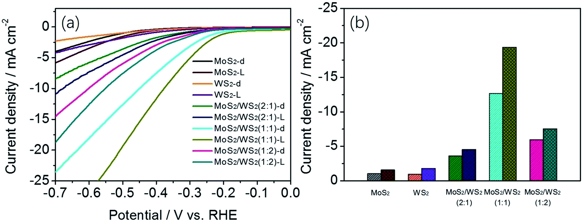 | ||
| Fig. 7 (a) J–V curves of cathodic polarization of MoS2, WS2 and MoS2/WS2 catalysts and (b) histogram of current density at −0.5 V (vs. RHE) of MoS2, WS2 with different Mo:W ratios in dark and under simulated solar light (0.5 M H2SO4). | ||
The photoelectrocatalytic activity for MoS2/WS2 hybrid was further evaluated by comparing its potential at −10 mA of photo-assistant current density with that from the related literature (Table 1).66–71 They are comparable, since all these catalyst samples were prepared in form of ultrathin film on a less conductive substrate except Au and GCE. From the Table 1, we found that vertically aligned MoS2/WS2 hybrid shows a better photo assistant electrocatalytic activity on both less conductive and conductive substrate. This improvement in catalytic activity derives from the characteristics of the vertical aligned ultrathin MoS2/WS2 sheets that integrate energy band alignment and abundant active sites of MoS2/WS2 catalyst. We also highlighted the photocatalytic activity of MoS2/WS2 through photocatalytic H2 production. The H2 evolution rates under light irradiation without any applied bias for MoS2/WS2/ITO manifests the rate of 0.049 ml h−1. It should be noted that the hydrogen evolution rate of 0.049 ml h−1 is produced from the ultrathin MoS2/WS2 layer of ∼223 nm (Fig. S11†) which dispersed uniformly on the 8 cm2 of surface area of ITO. For comparison with the previous studies, we have to convert ml h−1 to μmol g−1 h−1, a customary unit used for hydrogen production rate. It was revealed that the MoS2/WS2 hierarchical nanosheet possesses significantly high photocatalytic activity (>2065 μmol h−1 g−1). (ESI, Table S1†) noteworthy is, the estimated mass weight of MoS2/WS2 nanosheet is greater than the actual mass weight because the MoS2/WS2 structure is hierarchical and poriferous rather than solid, thus leading to an underestimate for H2 evolution production.
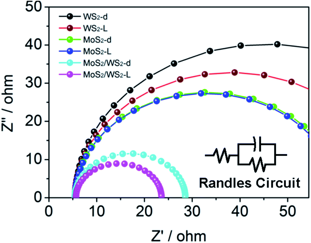
Furthermore, the surface kinetics of the as prepared catalysts was evaluated by EIS (Fig. 8). The diameter of the fitted semicircle represents the charge transfer resistance (Rct), which is inversely proportional to the rate of charge transfer in the HER process. In a Nyquist plot, the overlaying Nyquist plots of MoS2/WS2 (1/1) displayed a narrower semicircle diameter than that of WS2 or MoS2. In either case, in dark or under light illumination, the Rct values of MoS2 and WS2 are found to be much higher than MoS2/WS2 (17.92 Ω and 23.13 Ω under light illumination and in dark, respectively) (Fig. 8). Compared to WS2, or MoS2, (see Table 2), the significantly reduced Rct of MoS2/WS2 shows faster HER kinetics and better catalytic charge-transfer impedance. Undoubtedly, the faster HER surface kinetics of MoS2/WS2 produces a positive influence on photo- and electrocatalytic activity for HER.
 | ||
| Fig. 8 AC impedance spectroscopy of MoS2, WS2 and MoS2/WS2(1:1) catalysts in dark and under simulated solar light. | ||
| MoS2-d | MoS2-L | WS2-d | WS2-L | MoS2/WS2-d | MoS2/WS2-L | |
|---|---|---|---|---|---|---|
| Rct/Ω | 55.21 | 54.66 | 80.49 | 65.60 | 23.13 | 17.92 |
We also measured the electrochemically active surface area (ECSA) of the solid–liquid interfaces through electrochemical double-layer capacitance (EDLC) of the catalytic surface via CV.54 The EDLC values of MoS2, WS2 and MoS2/WS2 catalysts is 0.423, 0.245 and 3.05 mF cm−2, respectively, which is obtained by the slop of a straight line extracted from the capacitive current as a function of scan rate.72–74 As shown in Fig. S8c and f,† the EDLC value of 3.05 mF cm−2 for the MoS2/WS2 is much bigger than the values of MoS2 and WS2. (Fig. S8a–d and S8b–e,† respectively), indicating that MoS2/WS2 had the largest effective electrochemical area among the three catalysts, and thus presented more active sites.
4. Conclusion
MoS2/WS2 nanosheets with a vertically aligned structure fabricated directly on indium tin oxide (ITO) substrate were fabricated through a facile one-pot hydrothermal reaction. The hybrid nanosheets of MoS2/WS2 supplied numbers of active sites with proper defects since the elements of W doped MoS2. Favorable band alignment, as well as high-quality, intimate p–n heterojunction between MoS2 and WS2, provides an effective carrier separation in this composite based photoelectric device. Therefore, the MoS2/WS2 nanosheets show better visible light activities than that of either pristine WS2 or MoS2 nanostructures. The improvements in both electro- and photocatalytic activities for HER are ascribed to the integration of energy band alignment and abundant active sites derived of the vertically aligned MoS2/WS2 nanosheets. The rational use of the MoS2/WS2 cathode provided a new avenue toward achieving an enhanced electrocatalytic activity by photo-assistance.Conflicts of interest
There are no conflict to declare.References
- C. Tsai, F. Abild-Pedersen and J. K. Norskov, Nano Lett., 2014, 14, 1381–1387 CrossRef CAS PubMed.
- A. Ejigu, I. A. Kinloch, E. Prestat and R. A. W. Dryfe, J. Mater. Chem. A, 2017, 5, 11316–11330 CAS.
- H. Huang, L. Chen, C. Liu, X. Liu, S. Fang, W. Liu and Y. Liu, J. Mater. Chem. A, 2016, 4, 14577–14585 CAS.
- H. Zhou, F. Yu, J. Sun, R. He, Y. Wang, C. F. Guo, F. Wang, Y. Lan, Z. Ren and S. Chen, J. Mater. Chem. A, 2016, 4, 9472–9476 CAS.
- D. A. Reddy, H. Park, S. Hong, D. P. Kumar and T. K. Kim, J. Mater. Chem. A, 2017, 5, 6981–6991 CAS.
- T. An, Y. Wang, J. Tang, W. Wei, X. Cui, A. M. Alenizi, L. Zhang and G. Zheng, J. Mater. Chem. A, 2016, 4, 13439–13443 CAS.
- Y. Xu, L. Wang, X. Liu, S. Zhang, C. Liu, D. Yan, Y. Zeng, Y. Pei, Y. Liu and S. Luo, J. Mater. Chem. A, 2016, 4, 16524–16530 CAS.
- Q. Wang, Z. Liu, X. Zhang, H. Zhao, C. Luo, H. Jiao and Y. Du, J. Mater. Chem. A, 2017, 5, 9523–9527 CAS.
- W. Maijenburg, M. Regis, A. N. Hattori, H. Tanaka, K. S. Choi and J. E. Ten Elshof, ACS Appl. Mater. Interfaces, 2014, 6, 2003–2010 Search PubMed.
- Y. Yan, B. Xia, X. Qi, H. Wang, R. Xu, J. Y. Wang, H. Zhang and X. Wang, Chem. Commun., 2013, 49, 4884–4886 RSC.
- Y. Yan, B. Xia, X. Ge, Z. Liu, J. Y. Wang and X. Wang, ACS Appl. Mater. Interfaces, 2013, 5, 12794–12798 CAS.
- D. Voiry, M. Salehi, R. Silva, T. Fujita, M. Chen, T. Asefa, V. B. Shenoy, G. Eda and M. Chhowalla, Nano Lett., 2013, 13, 6222–6227 CrossRef CAS PubMed.
- F.-K. Meng, J.-T. Li, S. K. Cushing, M. Zhi and N.-Q. Wu, J. Am. Chem. Soc., 2013, 135, 10286–10289 CrossRef CAS PubMed.
- G. Morales-Guio, S. D. Tilley, H. Vrubel, M. Gratzel and X. Hu, Nat. Commun., 2014, 5, 3059 Search PubMed.
- H. V. a. X. Hu, ACS Catal., 2013, 3, 2002–2011 CrossRef.
- Y. Zhao, Y. Zhang, Z. Yang, Y. Yan and K. Sun, Sci. Technol. Adv. Mater., 2013, 14, 043501 CrossRef PubMed.
- D. Merki and X. Hu, Energy Environ. Sci., 2011, 4, 3878 CAS.
- S. Trasatti, J. Electroanal. Chem., 1971, 33, 350–378 Search PubMed.
- Sobczynski, A. Yildiz, A. J. Bard, A. Campion, M. A. Fox, T. Mallouk, S. E. Webber and J. M. White, J. Phys. Chem., 1988, 92, 2311–2315 CrossRef CAS.
- J. Bonde, P. G. Moses, T. F. Jaramillo, K. Nørskovb and I. Chorkendorff, Faraday Discuss., 2009, 140, 219–231 RSC.
- A.-B. Laursen, S. Kegnæs, S. Dahl and I. Chorkendorff, Energy Environ. Sci., 2012, 5, 5577–5591 CAS.
- Y.-G. Li, H.-L. Wang, L.-M. Xie, Y.-Y. Liang, G.-S. Hong and H.-J. Dai, J. Am. Chem. Soc., 2011, 133, 7296–7299 CrossRef CAS PubMed.
- J.-K. Lee, W. Lee, T.-J. Yoon, G.-S. Park and J.-H. Choy, J. Mater. Chem., 2002, 12, 614–618 RSC.
- Q. H. Wang, K. Kalantar-Zadeh, A. Kis, J. N. Coleman and M. S. Strano, Nat. Nanotechnol., 2012, 7, 699–712 CrossRef CAS PubMed.
- D. Jing and L. Guo, Catal. Commun., 2007, 8, 795–799 CrossRef CAS.
- X. Zong, J. Han, G. Ma, H. Yan, G. Wu and C. Li, J. Phys. Chem. C, 2011, 115, 12202–12208 CAS.
- Y. Zhong, G. Zhao, F. Ma, Y. Wu and X. Hao, Appl. Catal., B, 2016, 199, 466–472 CrossRef CAS.
- X. Zong, H. Yan, G. Wu, G. Ma, F. Wen, L. Wang and C. Li, J. Am. Chem. Soc., 2008, 130, 7176–7177 CrossRef CAS PubMed.
- K. Chang, Z. Mei, T. Wang, Q. Kang, S. Ouyang and J. Ye, ACS Nano, 2014, 8, 7078–7087 CrossRef CAS PubMed.
- R. Tang, R. Yin, S. Zhou, T. Ge, Z. Yuan, L. Zhang and L. Yin, J. Mater. Chem. A, 2017, 5, 4962–4971 CAS.
- X. Hong, J. Kim, Su-F. Shi, Y. Zhang, C. Jin, Y. Sun, S. Tongay, J. Wu, Y. Zhang and F. Wang, Nat. Nanotechnol., 2014, 9, 682 CrossRef CAS PubMed.
- K. Chen, X. Wan, W. Xie, J. Wen, Z. Kang, X. Zeng, H. Chen and J. Xu, Adv. Mater., 2015, 27, 6431–6437 CrossRef CAS PubMed.
- H. M. Hill, A. F. Rigosi, K. T. Rim, G. W. Flynn and T. F. Heinz, Nano Lett., 2016, 16, 4831–4837 CrossRef CAS PubMed.
- K. Kośmider and J. Fernández-Rossier, Phys. Rev. B: Condens. Matter Mater. Phys., 2013, 87, 075451 CrossRef.
- A. Kuc, N. Zibouche and T. Heine, Phys. Rev. B: Condens. Matter Mater. Phys., 2011, 83, 245213 CrossRef.
- B. Hinnemann, P. G. Moses, J. Bonde, K. P. Jørgensen, J. H. Nielsen, S. Horch, I. Chorkendorff and J. K. Nørskov, J. Am. Chem. Soc., 2005, 127, 5308–5309 CrossRef CAS PubMed.
- H. Tributsch and B. B. Gesell, Ber. Bunsen-Ges. Phys. Chem., 1977, 81, 361–369 CrossRef CAS.
- H. Tributsch and J. C. Bennett, J. Electroanal. Chem., 1977, 81, 97–111 CrossRef CAS.
- B. Hinnemann, J. K. Nørskov and H. Topsøe, J. Phys. Chem. B, 2005, 109, 2245–2253 CrossRef CAS PubMed.
- Z. Wu, B. Fang, A. Bonakdarpour, A. Sun, D. P. Wilkinson and D. Wang, Appl. Catal., B, 2012, 125, 59–66 CrossRef CAS.
- D. Voiry, H. Yamaguchi, J. Li, R. Silva, D. C. Alves, T. Fujita, M. Chen, T. Asefa, V. B. Shenoy, G. Eda and M. Chhowalla, Nat. Mater., 2013, 12, 850–855 CrossRef CAS PubMed.
- C. L. Choi, J. Feng, Y. Li, J. Wu, A. Zak, R. Tenne and H. Dai, Nano Res., 2013, 6, 921–928 CrossRef CAS.
- X. Hai, W. Zhou, K. Chang, H. Pang, H. Liu, L. Shi, F. Ichihara and J. Ye, J. Mater. Chem. A, 2017, 5, 8591–8598 CAS.
- Y. Yu, S. Huang, Y. Li, S. Steinmann, W. Yang and L. Cao, Nano Lett., 2014, 14, 553–558 CrossRef CAS PubMed.
- Z. Lu, W. Zhu, X. Yu, H. Zhang, Y. Li, X. Sun, X. Wang, H. Wang, J. Wang, J. Luo, X. Lei and L. Jiang, Adv. Mater., 2014, 26, 2683–2687 CrossRef CAS PubMed , 2615.
- Y. Yan, B. Xia, Z. Xu and X. Wang, ACS Catal., 2014, 4, 1693–1705 CrossRef CAS.
- Y. H. Chang, F. Y. Wu, T. Y. Chen, C. L. Hsu, C. H. Chen, F. Wiryo, K. H. Wei, C. Y. Chiang and L. J. Li, Small, 2014, 10, 895–900 CrossRef CAS PubMed.
- P. D. Tran, S. S. Pramana, V. S. Kale, M. Nguyen, S. Y. Chiam, S. K. Batabyal, L. H. Wong, J. Barber and J. Loo, Chemistry, 2012, 18, 13994–13999 CrossRef CAS PubMed.
- J.-F. Xie, H. Zhang, S. Li, R.-X. Wang, X. Sun, M. Zhou, J.-F. Zhou, X.-W. Lou and Y. Xie, Adv. Mater., 2013, 25, 5807–5813 CrossRef CAS PubMed.
- S.-K. Park, D. Y. Chung, D. Ko, Y.-E. Sung and Y. Piao, J. Mater. Chem. A, 2016, 4, 12720–12725 CAS.
- N. Zhang, S. Gan, T. Wu, W. Ma, D. Han and L. Niu, ACS Appl. Mater. Interfaces, 2015, 7, 12193–12202 CAS.
- Y. Sun, K. Liu, X. Hong, M. Chen, J. Kim, S. Shi, J. Wu, A. Zettl and F. Wang, Nano Lett., 2014, 14, 5329–5334 CrossRef CAS PubMed.
- Q. Ding, F. Meng, C. R. English, M. Caban-Acevedo, M. J. Shearer, D. Liang, A. S. Daniel, R. J. Hamers and S. Jin, J. Am. Chem. Soc., 2014, 136, 8504–8507 CrossRef CAS PubMed.
- A. Lukowski, A. S. Daniel, F. Meng, A. Forticaux, L. Li and S. Jin, J. Am. Chem. Soc., 2013, 10274–10277 CrossRef PubMed.
- U. Maitra, U. Gupta, M. De, R. Datta, A. Govindaraj and C. N. Rao, Angew. Chem., Int. Ed. Engl., 2013, 52, 13057–13061 CrossRef CAS PubMed.
- Q. Liu, X. Li, Q. He, A. Khalil, D. Liu, T. Xiang, X. Wu and L. Song, Small, 2015, 11, 5556–5564 CrossRef CAS PubMed.
- Q. Liu, X. Li, Z. Xiao, Y. Zhou, H. Chen, A. Khalil, T. Xiang, J. Xu, W. Chu, X. Wu, J. Yang, C. Wang, Y. Xiong, C. Jin, P. M. Ajayan and L. Song, Adv. Mater., 2015, 27, 4837–4844 CrossRef CAS PubMed.
- L. U. J. Bo, Z. Z. Wei and L. H. Gui, China Tungsten Ind., 2005, 20, 33–36 Search PubMed.
- G. Kulmukhamedov, A. Zelikman and G. Verevkin, Zh. Anal. Khim., 1991, 36, 2981–2985 CAS.
- B. E. Erickson and G. R. HELZ, Geochim. Cosmochim. Acta, 2000, 64, 1149–1158 CrossRef CAS.
- F. Wypych and R. Schöllhorn, J. Chem. Soc., Chem. Commun., 1992, 1386–1388 RSC.
- C. Liu, L. Wang, Y. Tang, S. Luo, Y. Liu, S. Zhang, Y. Zeng and Y. Xu, Appl. Catal., B, 2015, 164, 1–9 CrossRef CAS.
- S. Li, S. Wang, D.-M. Tang, W. Zhao, H. Xu, L. Chu, Y. Bando, D. Golberg and G. Eda, Applied Materials Today, 2015, 1, 60–66 CrossRef.
- S. Hernandez, D. Hidalgo, A. Sacco, A. Chiodoni, A. Lamberti, V. Cauda, E. Tresso and G. Saracco, Phys. Chem. Chem. Phys., 2015, 17, 7775–7786 RSC.
- J. O. M. Bockris and J. E. C. Potter, J. Electrochem. Soc., 1952, 99, 169–186 CrossRef CAS.
- X. Zhang, Y. Yang, S. Ding, W. Que, Z. Zheng and Y. Du, Inorg. Chem., 2017, 56, 3386–3393 CrossRef CAS PubMed.
- Y.-F. Zhao, Z.-Y. Yang, Y.-X. Zhang, L. Jing, X. Guo, Z.-T. Ke, P.-W. Hu, G.-X. Wang, Y.-M. Yan and K.-N. Sun, J. Phys. Chem. C, 2014, 118, 14238–14245 CAS.
- J. M. Woods, Y. Jung, Y. Xie, W. Liu, Y. Liu, H. Wang and J. J. Cha, ACS Nano, 2016, 10, 2004–2009 CrossRef CAS PubMed.
- Y. Qi, Q. Xu, Y. Wang, B. Yan, Y. Ren and Z. Chen, ACS Nano, 2016, 10, 2903–2909 CrossRef CAS PubMed.
- J. Shi, R. Tong, X. Zhou, Y. Gong, Z. Zhang, Q. Ji, Y. Zhang, Q. Fang, L. Gu, X. Wang, Z. Liu and Y. Zhang, Adv. Mater., 2016, 28, 10664–10672 CrossRef CAS PubMed.
- S. Xu, D. Li and P. Wu, Adv. Funct. Mater., 2015, 25, 1127–1136 CrossRef CAS.
- S. Trasatti and O. A. Petrii, Pure Appl. Chem., 1991, 63, 711–734 CrossRef CAS.
- J. D. Benck, Z. Chen, L. Y. Kuritzky, A. J. Forman and T. F. Jaramillo, ACS Catal., 2012, 2, 1916–1923 CrossRef CAS.
- R. Boggio, A. Garugati and S. Trasatti, J. Appl. Electrochem., 1987, 17, 828–840 CrossRef CAS.
- S. J. Hong, S. Lee, J. S. Jang and J. S. Lee, Energy Environ. Sci., 2011, 4, 1781 CAS.
- H. Huang, D. Li, Q. Lin, W. Zhang, Y. Hao, Y. Chen, M. Sun and A. Fu, Environ. Sci. Technol., 2009, 43, 4164–4168 CrossRef CAS PubMed.
Footnote |
| † Electronic supplementary information (ESI) available. See DOI: 10.1039/c7ra10762e |
| This journal is © The Royal Society of Chemistry 2017 |