
 Open Access Article
 This Open Access Article is licensed under a
 Creative Commons Attribution 3.0 Unported Licence
Graphene sandwiched platform for surface-enhanced Raman scattering†
Yuan Zhao *a,
Xiyu Lib,
Lichun Zhanga,
Binhua Chua,
Qiyi Liuc and
Yalin Lubd
*a,
Xiyu Lib,
Lichun Zhanga,
Binhua Chua,
Qiyi Liuc and
Yalin Lubd
aSchool of Physics and Optoelectronic Engineering, Ludong University, Yantai 264025, China. E-mail: yzhaol@mail.ustc.edu.cn
bSchool of Chemistry and Materials Science, University of Science and Technology of China, Hefei, 230026, China
cSchool of Food Engineering, Ludong University, Yantai 264025, China
dLaser Optics Research Center, Physics Department, United States Air Force Academy, Colorado 80840, USA
First published on 23rd October 2017
Abstract
The graphene–plasmonic metal nanoparticle (NP) hybrid system has attracted much attention for its potential capacity to be used as surface-enhanced Raman scattering (SERS) substrate. Here, we fabricated a SERS substrate by sandwiching monolayer graphene (1LG) between gold (Au) NPs and silver (Ag) nanoarrays (NAs). With modulation of the structural parameters, we have obtained Ag NAs with a gap between the flower-shaped Ag particles as small as 14 nm. Finite element numerical simulations revealed that the Au NP–graphene–Ag NA structure generates high-density hot spots with strong electric field enhancement through the couplings of plasmonic metal NPs. Benefit from the strong electric field enhancement and chemical enhancement, the prepared Au NP–1LG–Ag NA hybrid structure exhibited excellent SERS activity of high sensitivity with the detection limit as low as 0.1 pM for Rhodamine 6G. Moreover, we has achieved the simultaneous detection for both methylene blue and Rhodamine 6G molecules by using the as-prepared Au NP–1LG–Ag NA structure. These results may render the graphene-sandwiched hybrid system to function as a promising tool for SERS sensing applications.
1. Introduction
Surface-enhanced Raman scattering (SERS) is a powerful sensing technique for the ultra-sensitive detection and identification of chemical and biological species.1–3 A variety of plasmonic metal nanostructures have been employed to achieve high sensitivity for the excitation of surface plasmons with strong electromagnetic (EM) enhancement (also called “hot spots”). The EM hot spots are mainly distributed near the sharp asperities and gaps between metal nanoparticles (NPs).4,5 It is demonstrated that the EM enhancement can be amplified by decreasing interparticle gaps since the enhanced EM field is inversely proportional to the distance between metal NPs.6 In efforts to engineer small interparticle gaps, various metal nanostructures, such as nanowire-nanoparticles,7 dimers,8 ring-disks,9 have been designed and fabricated to improve the SERS sensing sensitivity. However, the weak controllability of metal NPs and/or poor reliability of SERS signals often restricted the practical applications. Previously, although Al2O3 and SiO2 have been used to construct vertical gaps,10,11 the precise control of nanostructures for generating uniform nanometer-scale spaces remains experimentally challenging. Moreover, in these structures, efficient adsorbing of molecules are inaccessible due to the weak affinity between the substrates and molecules.Graphene, a one-atom-thick planar sheet of carbon atoms arranged in a two-dimensional hexagonal lattice, has been attracting tremendous interest since it was experimentally exfoliated in 2004.12 It has excellent features of atomic-scale thickness, chemical stability, mechanical flexibility and biological compatability.13 Graphene itself can be used as a Raman substrate with an enhancement factor in the range of 10–100 through chemical enhancement.14 Inspiringly, the graphene–metal NP hybrid systems hold great promise for constructing high-sensitivity SERS substrate by integrating EM enhancement and chemical enhancement. Previously, graphene–metal bilayers, including covering graphene on the surface of metal nanostructures or depositing metal NPs on graphene, were prepared and used as SERS substrates.15,16 It was indicated that graphene can act as an insulating spacer by embedding it between two metal layers for its high vertical resistance.17,18 Wu et al.19 theoretically demonstrated that the coupling of metal NPs on the opposite sides of graphene can generate several orders of magnitude larger electric field enhancement than those without coupling. Recently, the sandwich structures with graphene (or graphene oxide, or reduced graphene oxide) embedded between two layers of metal structures have been prepared for improving SERS sensitivity.20–22 Nevertheless, a uniform nanometer-scale graphene spacer was not easily achieved due to the stacking of graphene oxide/reduced graphene oxide layer and/or unordered dispersions of metal NPs, thereby limiting the reproducibility of SERS signals. Thus, it is desirable to develop an effective method to fabricate graphene–metal NP sandwich structures with much more controlled manner. Electron beam lithography (EBL) is an effective method to fabricate ordered structure as it enables the precise control of the shape and size of particles.23,24 On the other hand, a low-velocity deposition of thin metal films and an annealing process can generate high-density metal NPs with a weak wear for graphene films.25
Herein we prepared a uniform gold (Au) NP–monolayer graphene (1LG)–silver nanoarray (Ag NA) structure by embedding single layer graphene between Au NPs and EBL-fabricated flower-shaped Ag NAs. In this structure, the sandwich configuration has integrated the high orderness and uniformity of Ag NAs, the single-atomic thickness and biological compatibility of graphene, as well as the stability of Au. By tuning the size of the structure written by electron-beam (E-beam), we have obtained Ag NAs with interparticle space of 14 nm. Finite element numerical simulations revealed that the Au NP–1LG–Ag NA hybrid structure boosts high-density hot spots with strong electric field enhancement through the coupling of the top Au NPs and the bottom Ag NAs. The fabricated Au NP–1LG–Ag NA hybrid structure has exhibited excellent SERS activity of high sensitivity, and achieved the simultaneous detection of methylene blue (MB) and rhodamine 6G (R6G) molecules.
2. Experimental section
2.1 Fabrication of the Au NP–1LG–Ag NA structure
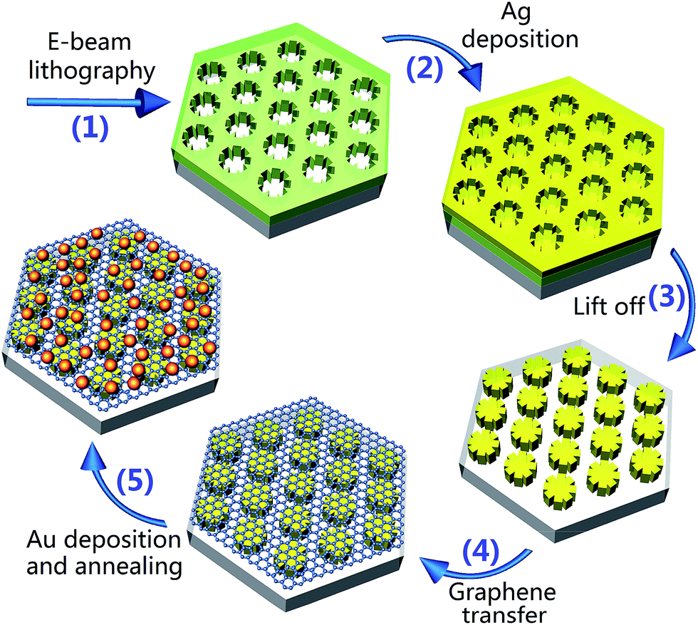
The fabrication procedure for the Au NP–1LG–Ag NA structure is depicted in Fig. 1. Firstly, a 260 nm-thick polymethyl methacrylate (PMMA) layer was spin-coated on Si and backed at 180 °C for 90 s on a hot plate in order to evaporate the solvent in the resist. A flower-shaped array pattern was written by EBL system (JEOL JBX-6300FS), which is operated at 100 kV accelerating voltage with an area dosage of 800 μC cm−2 and a current of 100 pA, and thus forming a flower-shaped PMMA nanohole array after the developing in a solution of methyl isobutyl ketone (MIBK) and isopropanol (IPA) with 1![[thin space (1/6-em)]](https://www.rsc.org/images/entities/char_2009.gif) :3 mixture ratio for 60 s and rinsing in IPA for 60 s26,27 (step 1). Then, 5 nm-thick Cr adhesion layer (0.5 Å s−1) and 40 nm-thick Ag layer (1 Å s−1) were sequentially deposited on the surface of the prepared sample by magnetic sputtering (step 2). With a lift-off process via immersing the sample in acetone, we obtained an ordered Ag–Gr NA (step 3). For convenience, we call them Ag NAs. In the next step, monolayer graphene films grown on Cu foils were transferred onto the prepared Ag NAs, thereby achieving 1LG–Ag NA structure (step 4). Finally, a 5 nm-thick Au film (0.5 Å s−1) was deposited onto the surface of 1LG–Ag NA and annealed with flowing Ar at 300 °C for 60 min, forming Au NP–1LG–Ag NA sandwich structure (step 5).
:3 mixture ratio for 60 s and rinsing in IPA for 60 s26,27 (step 1). Then, 5 nm-thick Cr adhesion layer (0.5 Å s−1) and 40 nm-thick Ag layer (1 Å s−1) were sequentially deposited on the surface of the prepared sample by magnetic sputtering (step 2). With a lift-off process via immersing the sample in acetone, we obtained an ordered Ag–Gr NA (step 3). For convenience, we call them Ag NAs. In the next step, monolayer graphene films grown on Cu foils were transferred onto the prepared Ag NAs, thereby achieving 1LG–Ag NA structure (step 4). Finally, a 5 nm-thick Au film (0.5 Å s−1) was deposited onto the surface of 1LG–Ag NA and annealed with flowing Ar at 300 °C for 60 min, forming Au NP–1LG–Ag NA sandwich structure (step 5).
 | ||
| Fig. 1 Schematic fabrication process for the Au NP–1LG–Ag NA sandwich structure. | ||
2.2 Structural characterization and Raman detection
The prepared structures were characterized using scanning electron microscopy (SEM) and atomic force microscopy (AFM). Raman spectra were measured using Renishaw inVia Raman Microscope. The wavelength of laser was 532 nm. A× 50 objective was used and the laser spot was ∼1 μm2. The integration time is 1 s. The laser power was set to be 5 mW for measuring graphene and 0.5 mW for measuring dye molecules for protecting the sample from possible heating and photo-induced damages. For measuring the Raman signals of molecules, a 10 μL droplet was dispersed on the as-prepared substrates and dried in air. Here, R6G solutions were obtained by dissolving the solid powders and diluting using ethanol. The mixture solution of MB and R6G was obtained by dissolving both the MB and R6G powders in ethanol.2.3 Finite element numerical simulations
The plasmonic electric field enhancement effect of the structures was investigated by utilizing the software package “Comsol Multiphysics”.28–30 In the vertical directions, we used absorbing boundary conditions for eliminating the undesired reflections from boundaries, and in the horizontal directions, we set periodic boundary conditions for simulating a single unit cell. The dielectric constant of graphene was calculated by n = 3 + c(λ/3)i (c = 5.446 μm−1 and λ was the wavelength)31 and the optical parameters of Au and Ag were obtained using Drude model.32 The dielectric constant of Si was 13.39. Convergence mesh analysis was used to achieve stationary results. The mesh maximum element size was set as 0.2 nm in the domains representing graphene, 4 nm in Au NPs, 8 nm in Ag particles and 12 nm for all the elements in the air and substrate subdomains.3. Results and discussion
3.1 Structural characterization
The fabrication method of Ag NAs provides a favorable test bed for tuning the plasmonic properties and better transfer of grapheme films. Fig. 2 shows the AFM images of Ag NAs with or without graphene covered on the structure surface for three different lattice periods (the distance between the adjacent Ag particles in the longitudinal direction). For the pattern written, the length of the octagonal flowers was fixed to be 180 nm, and the distance between the adjacent two columns was equal to the lattice period. The thickness of Ag deposited was 40 nm. As shown, the patterned flower-shaped Ag NAs exhibit good uniformity and orderness. With a control of the structural parameter, we have obtained Ag NAs with lattice period of 241 nm (Fig. 2a), 222 nm (Fig. 2b) and 209 nm (Fig. 2c), respectively. Since the size and shape of the Ag flowers keep consistent in all the structures, the interparticle gap was minished with the decrease of lattice period, allowing for Ag NAs with interparticle gap of 61 nm (Fig. 2a), 42 nm (Fig. 2b) and 29 nm (Fig. 2c), respectively. Importantly, the Ag NAs with small interparticle gaps have a positive effect on the transfer of graphene films. From the AFM images of 1LG–Ag NA structure, we can see the dropping of graphene films along the seams of Ag NAs and small amount of wear-and-tear after placing graphene on Ag NAs with interparticle gap of 61 nm (Fig. 2d) and 42 nm (Fig. 2e), while the graphene films exhibit better flatness with the coverage of graphene films onto Ag NAs with interparticle gap of 29 nm (Fig. 2f).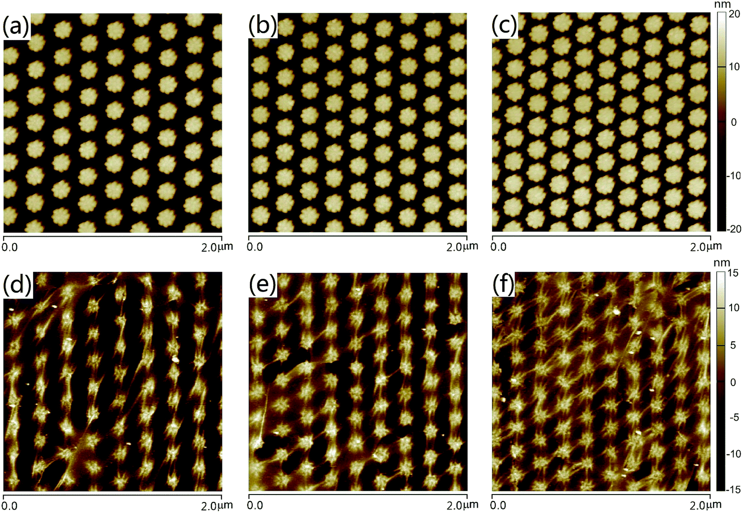 | ||
| Fig. 2 AFM images of (a–c) Ag NAs and (d–f) 1LG–Ag NA structures with lattice period of Ag NAs to be (a, d) 241 nm, (b, e) 222 nm and (c, f) 209 nm, respectively. | ||
By further tuning the structure parameter of the patterned arrays, Ag NAs with higher particle density have been fabricated. As indicated by the SEM and AFM images, we have achieved Ag NAs with lattice period of 194 nm and interparticle gap of 14 nm (Fig. 3a and b). Fig. 3c and d depicts the SEM and AFM images of 1LG–Ag NA structure. It can be seen that the graphene films exhibit good completeness in a large scale after being transferred onto the Ag NAs, implying the flexibility of graphene when it was integrated with ordered Ag NAs. After a 5 nm-thickness Au film was deposited and annealed on the as-prepared 1LG–Ag NA surface, Au NP–1LG–Ag NA structure was obtained (Fig. 3e and f). Here, the formation of Au NPs can be ascribed to the spatial reactivity with nucleation and growth of nanometer-scale particles during the annealing process.33,34 From the AFM image of Au NP–1LG–Ag NA structure (Fig. 3f), we can see that the Au NPs are packed closely, in which graphene film functions as an important supporting layer between the top Au NPs and the bottom Ag NAs. In contrast, the Au NP–Ag NA structure reveals a similar morphology to bare Ag NAs (Fig. S1, ESI†). The diameter of the Au NPs is ∼32 nm and the distance between the adjacent Au NPs is ∼40 nm (Fig. S2, ESI†). Here, the fabricated Au NP–1LG–Ag NA hybrid system has integrated the orderness and uniformity of Ag NAs, the single-atomic feature and biological compatibility of graphene, as well as the chemical stability of Au, which are all beneficial to promote SERS sensing capacity.
 | ||
| Fig. 3 (a, c, e) SEM and (b, d, f) AFM images of (a, b) Ag NAs, (c, d) 1LG–Ag NA and (e, f) Au NP–1LG–Ag NA structures with lattice period of Ag NAs to be 194 nm. The enlarged view of Ag NAs in (a) indicates that the gap between the adjacent Ag particles is ∼14 nm. | ||
3.2 Electric field enhancement effects
Fig. 4a shows the simulation configuration of Au NP–graphene–Ag NA. The length of the octagonal flowers is 180 nm, and the thickness is 40 nm. The outer edges of the octagonal flowers are slightly rounded for matching the shape of the actual structures. The lattice period of Ag NAs is 194 nm, the lateral and longitudinal sizes of the unit cell are both 388 nm. The thickness of graphene layer sandwiched between Au NPs and Ag NAs is 1 nm. This value is reasonable by considering the inhomogeneity of graphene in the growth and transfer processes.35 The diameter of Au NPs is 34 nm and the distance between the adjacent Au NPs in the x and y directions are both 40 nm for mimicking the dimension of Au NPs in the experiments. A plane lightwave with a polarized electric field Ey was launched normally from the top. Fig. 4b–c illustrate the electric field intensity distributions of three different structures. As depicted in Fig. 4b for bare Ag NAs, the enhanced electric field is mainly confined in the inter-flower gaps. With graphene film covered on the surface of Ag NAs, a similar electric filed enhancement effect is observed (Fig. 4c), demonstrating a negligible attenuation of the plasmonic electric field enhancement for the excellent penetrability of graphene. In detail, the maximal electric field enhancements are 12 or 11 for Ag NAs or graphene–Ag NA structures, respectively. With graphene sandwiched between Au NPs and Ag NAs, the Au NP–graphene–Ag NA structure exhibits multiple hot spots with dramatically strong electric field enhancement (Fig. 4d). Here, the sandwich structure has taken the advantage of the single-atomic feature of graphene for creating nanometer-scale gaps, thereby leading to an electric field enhancement maximum of 91. Moreover, the graphene layer could promote the plasmonic coupling between the top Au NPs and the bottom Ag NAs.36 Since the EM field-excited Raman signal enhancement is proportional to (E/E0)4,25,37 the prepared sandwich structure may promote the SERS sensing.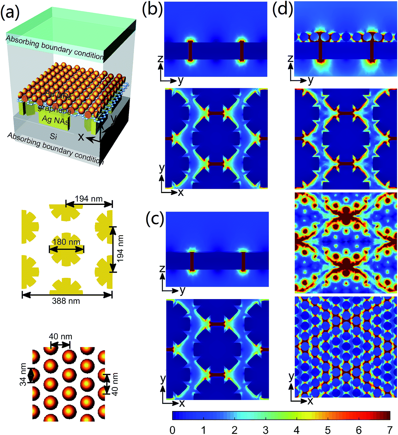 | ||
| Fig. 4 (a) Simulation configuration of Au NP-graphene–Ag NA on Si substrate. The length of the octagonal flowers is 180 nm, the thickness is 40 nm, the lattice period is 194 nm, the lateral and longitudinal sizes of the unit cell are both 388 nm. The outer edges of the octagonal flowers are slightly rounded for matching the shape of the actual structures. The diameter of Au NPs is 34 nm and the distance between the adjacent Au NPs in the x and y directions are both 40 nm. The thickness of graphene films is 1 nm. Normalized electric field intensity distributions for (b) Ag NAs in the yz plane at x = 194 nm and in the xy plane at z = 20 nm, (c) graphene–Ag NA in the yz plane at x = 194 nm and in the xy plane at z = 20 nm, and (d) Au NP–graphene–Ag NA structure in the yz plane at x = 194 nm and in the xy plane inside the bottom Ag NAs layer with z = 20 nm, inside the graphene layer with z = 40.5 nm and inside the top Au NPs layer with z = 58 nm, respectively. | ||
3.3 SERS detection
Fig. 5a shows the SERS spectra of graphene for 1LG–Ag NA and Au NP–1LG–Ag NA structures. The G peak around 1580 cm−1 (the doubly degenerate zone center E2g mode) and 2D peak around 2690 cm−1 (the second order of zone boundary phonons)38 are observed for both the samples. The D peak around 1350 cm−1 with low intensity demonstrates a few defects or adsorbents remaining for the transferred graphene films.34 Impressively, the Au NP–1LG–Ag NA structure has exhibited 15-fold stronger Raman signal for the G peak of graphene than that of 1LG–Ag NA structure for the extremely strong electric field enhancement through the multi-dimensional couplings of plasmonic metal NPs. The SERS spectra of graphene measured from five randomly selected spots confirm the uniform coverage or embedding of graphene in 1LG–Ag NA and Au NP–1LG–Ag NA structures (Fig. S3, ESI†).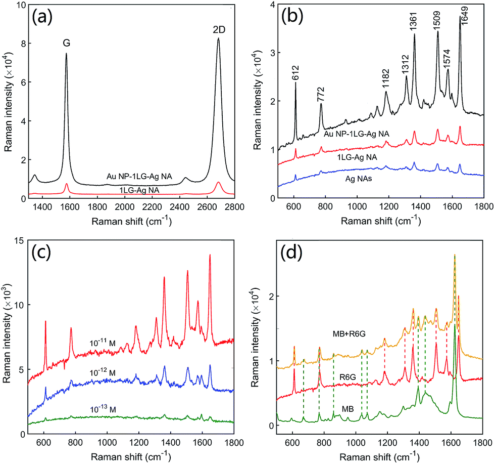 | ||
| Fig. 5 (a) SERS spectra of single layer graphene for 1LG–Ag NA and Au NP–1LG–Ag NA structures. (b) SERS spectra of 10−10 M R6G on Ag NAs, 1LG–Ag NA and Au NP–1LG–Ag NA structures. (c) SERS spectra of R6G on Au NP–1LG–Ag NA substrate for the molecular concentration of 10−11 M, 10−12 M and 10−13 M. (d) SERS spectra of 10−10 M MB, 10−11 M R6G and a mixture of 10−10 M MB and 10−11 M R6G on Au NP–1LG–Ag NA substrate. | ||
Fig. 5b shows the SERS spectra of 10−10 M R6G on Au NP–1LG–Ag NA structure. As references, the SERS sensing properties of R6G on Ag NAs and 1LG–Ag NA structures were also measured and shown in the same figure. As indicated, all the quintessential characteristic peaks of R6G including 612, 772, 1361, 1509 and 1649 cm−1 are observed in three substrates, and in agreement with those reported previously.39 When compared to Ag NAs, the Au NP–1LG–Ag NA substrate has exhibited 11.7 times larger intensity of SERS signal based on 1649 cm−1. The 2.2-fold enhancement for the SERS signal intensity of R6G on 1LG–Ag NA substrate than Ag NAs can be explained by the chemical enhancement arising from π–π interactions and charge transfer between graphene and R6G molecules.14,40 Besides the chemical enhancement, the extremely high SERS sensitivity for the Au NP–1LG–Ag NA system can be accounted for the excitation of high-density hot spots with strongly enhanced electric field. The SERS spectra of R6G at ten different spots of the Au NP–1LG–Ag NA substrate (Fig. S4, ESI†) evidence the good uniformity in device fabrication as well as the adsorption of molecules over the substrate. By decreasing the concentration of R6G solutions, we found that the Raman peaks of R6G on the prepared Au NP–1LG–Ag NA sandwich substrate can still be detected when the molecular concentration is down to 0.1 pM (Fig. 5c and S5, ESI†). Therefore, the designed and fabricated Au NP–1LG–Ag NA sandwich substrate exhibits excellent SERS activity of high sensitivity and good reproducibility. The prepared Au NP–1LG–Ag NA substrate was also used to detect the SERS signal of a mixture solution of 10−10 M MB and 10−11 M R6G. From the SERS spectra depicted in Fig. 5d, we can see that the vibrational modes of MB (1395 and 1624 cm−1)41 and the characteristic peaks of R6G (612, 1361, 1509 and 1649 cm−1) were simultaneously detected. This shows a potential for the practical applications in the areas of food safety, environmental monitoring, medical diagnostics, and biological sensing.
4. Conclusions
In conclusion, we have prepared a sandwiched Au NP–1LG–Ag NA structure by embedding monolayer graphene between Au NPs and EBL-fabricated Ag NAs. Finite element numerical simulations demonstrate that the Au NP–1LG–Ag NA structure generates high-density hot spots with strong electric field enhancement through the couplings of plasmonic metal NPs. With the electric field enhancement and chemical enhancement, the as-prepared Au NP–1LG–Ag NA hybrid system has exhibited excellent SERS activity of high sensitivity (the detection limit is 0.1 pM) and good reproducibility. By using the Au NP–1LG–Ag NA sandwich structure, we has achieved the simultaneous detection of MB and R6G molecules. These results show that the graphene-sandwiched hybrid system may function as a promising tool for SERS sensing applications.Conflicts of interest
There are no conflicts to declare.Acknowledgements
We gratefully acknowledge Chenggang Zhou, Kun Zhang, Dianfa Zhou, Xiuxia Wang, Jinlan Peng, Linjun Wang and Haibin Zhang from the USTC Center for Micro and Nanoscale Research and Fabrication for the technical support. We appreciate the financial support from the National Natural Science Foundation of China (No. 61705097, No. 11704170), the Natural Science Foundation of Shandong Province (No. ZR2016EMP01, No. ZR2016AP02, No. ZR2016AP07) and the Innovation Project of Ludong University (No. LA 2016003).Notes and references
- S. M. Nie and S. R. Emery, Science, 1997, 275, 1102–1106 CrossRef CAS PubMed.
- X. Li, J. Zhu and B. Wei, Chem. Soc. Rev., 2016, 45, 3145–3187 RSC.
- J.-F. Li, Y.-J. Zhang, S.-Y. Ding, R. Panneerselvam and Z.-Q. Tian, Chem. Rev., 2017, 117, 5002–5069 CrossRef CAS PubMed.
- S. Zhang, R. Geryak, J. Geldmeier, S. Kim and V. V. Tsukruk, Chem. Rev., 2017 DOI:10.1021/acs.chemrev.7b00088.
- K. A. Willets, Chem. Soc. Rev., 2014, 43, 3854–3864 RSC.
- H. Wei and H. Xu, Nanoscale, 2013, 5, 10794–10805 RSC.
- H. Wei, F. Hao, Y. Huang, W. Wang, P. Nordlander and H. Xu, Nano Lett., 2008, 8, 2497–2502 CrossRef CAS PubMed.
- M. Chirumamilla, A. Toma, A. Gopalakrishnan, G. Das, R. P. Zaccaria, R. Krahne, E. Rondanina, M. Leoncini, C. Liberale, F. De Angelis and E. Di Fabrizio, Adv. Mater., 2014, 26, 2353–2358 CrossRef CAS PubMed.
- F. Hao, P. Nordlander, Y. Sonnefraud, P. Van Dorpe and S. A. Maier, ACS Nano, 2009, 3, 643–652 CrossRef CAS PubMed.
- S. Mubeen, S. Zhang, N. Kim, S. Lee, S. Kraemer, H. Xu and M. Moskovits, Nano Lett., 2012, 12, 2088–2094 CrossRef CAS PubMed.
- D. Wang, W. Zhu, M. D. Best, J. P. Camden and K. B. Crozier, Sci. Rep., 2013, 3, 2867 CrossRef PubMed.
- K. S. Novoselov, A. K. Geim, S. V. Morozov, D. Jiang, Y. Zhang, S. V. Dubonos, I. V. Grigorieva and A. A. Firsov, Science, 2004, 306, 666–669 CrossRef CAS PubMed.
- W. Xu, N. Mao and J. Zhang, Small, 2013, 9, 1206–1224 CrossRef CAS PubMed.
- X. Ling, S. X. Huang, S. B. Deng, N. N. Mao, J. Kong, M. S. Dresselhaus and J. Zhang, Acc. Chem. Res., 2015, 48, 1862–1870 CrossRef CAS PubMed.
- P. Wang, O. Liang, W. Zhang, T. Schroeder and Y.-H. Xie, Adv. Mater., 2013, 25, 4918–4924 CrossRef CAS PubMed.
- C. Qiu, H. Zhou, B. Cao, L. Sun and T. Yu, Carbon, 2013, 59, 487–494 CrossRef CAS.
- K. J. Lee, D. Kim, B. C. Jang, D.-J. Kim, H. Park, D. Y. Jung, W. Hong, T. K. Kim, Y.-K. Choi and S.-Y. Choi, Adv. Funct. Mater., 2016, 26, 5093–5101 CrossRef CAS.
- Y. B. Zhang, Y. W. Tan, H. L. Stormer and P. Kim, Nature, 2005, 438, 201–204 CrossRef CAS PubMed.
- J. Wu, Y. Xu, P. Xu, Z. Pan, S. Chen, Q. Shen, L. Zhan, Y. Zhang and W. Ni, Nanoscale, 2015, 7, 17529–17537 RSC.
- X. Li, W. C. H. Choy, X. Ren, D. Zhang and H. Lu, Adv. Funct. Mater., 2014, 24, 3114–3122 CrossRef CAS.
- Y. Zhao, X. Li, Y. Du, G. Chen, Y. Qu, J. Jiang and Y. Zhu, Nanoscale, 2014, 6, 11112–11120 RSC.
- A. Liu, T. Xu, J. Tang, H. Wu, T. Zhao and W. Tang, Electrochim. Acta, 2014, 119, 43–48 CrossRef CAS.
- N. A. Abu Hatab, J. M. Oran and M. J. Sepaniak, ACS Nano, 2008, 2, 377–385 CrossRef CAS PubMed.
- A. W. Clark, A. Glidle, D. R. S. Cumming and J. M. Cooper, J. Am. Chem. Soc., 2009, 131, 17615–17619 CrossRef CAS PubMed.
- W. Xu, X. Ling, J. Xiao, M. S. Dresselhaus, J. Kong, H. Xu, Z. Liu and J. Zhang, Proc. Natl. Acad. Sci. U. S. A., 2012, 109, 9281–9286 CrossRef CAS PubMed.
- R. Palankar, N. Medvedev, A. Rong and M. Delcea, ACS Nano, 2013, 7, 4617–4628 CrossRef CAS PubMed.
- Y. Zhao, D. Yang, X. Li, Y. Liu, X. Hu, D. Zhou and Y. Lu, Nanoscale, 2017, 9, 1087–1096 RSC.
- COMSOL 4.3a Reference Manual, 2012, 4.3 Search PubMed.
- T.-T. Zhuang, Y. Liu, Y. Li, Y. Zhao, L. Wu, J. Jiang and S.-H. Yu, Angew. Chem., Int. Ed., 2016, 55, 6396–6400 CrossRef CAS PubMed.
- Y. Zhao, G. Chen, Y. Du, J. Xu, S. Wu, Y. Qu and Y. Zhu, Nanoscale, 2014, 6, 13754–13760 RSC.
- M. Bruna and S. Borini, Appl. Phys. Lett., 2009, 94, 031901 CrossRef.
- E. J. Zeman and G. C. Schatz, J. Phys. Chem., 1987, 91, 634–643 CrossRef CAS.
- R. R. Nair, P. Blake, A. N. Grigorenko, K. S. Novoselov, T. J. Booth, T. Stauber, N. M. R. Peres and A. K. Geim, Science, 2008, 320, 1308 CrossRef CAS PubMed.
- G. Xu, J. Liu, Q. Wang, R. Hui, Z. Chen, V. A. Maroni and J. Wu, Adv. Opt. Mater., 2012, 24, OP71–OP76 CrossRef CAS PubMed.
- X. Zhu, L. Shi, M. S. Schmidt, A. Boisen, O. Hansen, J. Zi, S. Xiao and N. A. Mortensen, Nano Lett., 2013, 13, 4690–4696 CrossRef CAS PubMed.
- N. Yi, C. Zhang, Q. Song and S. Xiao, Sci. Rep., 2016, 6, 25134 CrossRef CAS PubMed.
- H. Ko, S. Singamaneni and V. V. Tsukruk, Small, 2008, 4, 1576–1599 CrossRef CAS PubMed.
- A. C. Ferrari, J. C. Meyer, V. Scardaci, C. Casiraghi, M. Lazzeri, F. Mauri, S. Piscanec, D. Jiang, K. S. Novoselov, S. Roth and A. K. Geim, Phys. Rev. Lett., 2006, 97, 187401–187404 CrossRef CAS PubMed.
- L. Zhang, C. Jiang and Z. Zhang, Nanoscale, 2013, 5, 3773–3779 RSC.
- X. Yu, W. Zhang, P. Zhang and Z. Su, Biosens. Bioelectron., 2017, 89, 72–84 CrossRef CAS PubMed.
- G. Lu, H. Li, C. Liusman, Z. Yin, S. Wu and H. Zhang, Chem. Sci., 2011, 2, 1817–1821 RSC.
Footnote |
| † Electronic supplementary information (ESI) available. See DOI: 10.1039/c7ra10401d |
| This journal is © The Royal Society of Chemistry 2017 |