DOI:
10.1039/C7RA10416B
(Paper)
RSC Adv., 2017,
7, 51711-51720
Rapid and efficient intense pulsed light reduction of graphene oxide inks for flexible printed electronics
Received
20th September 2017
, Accepted 25th October 2017
First published on 7th November 2017
1. Introduction
Research on flexible electronics is rapidly expanding,1 and they exhibit applications in super-capacitors,2 sensors,3 electronic paper,4 solar cells,5 touch panels,6 and wireless wearable communication.7 Among current manufacturing techniques, drop-on-demand inkjet printing has been continuously investigated as the most promising technique in large-area manufacturing of flexible plastic electronics,8 and a series of components, such as chemical sensors,9 wideband dipole antennas,10 field-effect transistors,11 and electronic displays,12 can be printed. The significant advantages of this technique involve low cost, few processing steps, additive and digital patterning, low material consumption, and compatibility with various substrates.4,13–15 In printed materials, graphene has been a prominent contender as a printed metallic component because of its high conductivity, high transmittance, satisfactory stability, and inherent flexibility.16,17 However, there are sequences of issues that still need to be solved. First, the solvents, such as dimethylformamide (DMF) and N-methylpyrrolidone (NMP), in which graphene is dispersed, usually have a low viscosity (<2 cP), and stabilizers, such as ethyl cellulose (EC), are always needed. These stabilizers cannot meet the requirement of inks used for inkjet printing and make the preparation of the inks complex. Second, NMP and DMF are toxic and their corresponding inks are detrimental to the environment. Third, the concentration of graphene in solvents is usually low, and graphene aggregates easily in inks; this negatively affects the property and stability of the ink.11,15–18 Thus, research on graphene oxide (GO) as an ink material has been extensively conducted.19–21 GO has functionalized oxygen-containing groups on edges and basal planes; this makes GO easy to suspend in water or other organic solvents without any additional stabilized polymers and remain stable for a long time.10,22 However, conductivity of GO is far lower than that of graphene, and it needs additional reduction processing, such as use of a reducing agent20 and annealing,23 to restore its structure and obtain high conductivity.19 In 2014, Chi24 et al. synthesized a freestanding nanohybrid paper by inkjet printing, and the paper was reduced to a graphene paper-supported three-dimensional porous graphene hydrogel–polyaniline nanocomposite in a HI solution; moreover, the flexible all-solid-state supercapacitor fabricated using this nanocomposite exhibited excellent flexibility and acceptable energy density. In 2015, Xiao25 et al. utilized the reducing agent HI solution to develop the RGO/PANI/RGO sandwich-structured nanohybrid paper. It revealed high conductivity, lightweight, excellent mechanical property, and chemical stability, making it a potential material for supercapacitors and active electrodes. However, common reducing agents are poisonous,21 and annealing reduction is not suitable for temperature-sensitive substrates such as polyethylene terephthalate (PET), and polyimide (PI).20
IPL technology is carried out under low temperature, selective, and non-contact conditions. Using wideband spectrum and high energy pulsed light, ink materials on various substrates can be sintered and processed to realize functionality.26 In 2011, Kang27 et al. of the Hahn research group studied sintering of the silver-nanoparticle inks by intense pulsed light at room temperature. By adjusting the powers and the numbers of pulses, the silver electrode was completely sintered, and a combination of well binding ability with a low resistivity of 50 nΩ m was realized. In 2015, Secor28 et al. sintered a graphene-based ink printed on the flexible substrate PET by intense pulsed light. They produced inkjet-printable graphene-based inks with high concentrations of up to 20 mg ml−1 and realized excellent conductivity of 25![[thin space (1/6-em)]](https://www.rsc.org/images/entities/char_2009.gif) 000 S m−1 after one printing pass with pulsed light sintering. Thus, the IPL technology has great potential in printed electronics. However, research on the application of the IPL method for the reduction of GO ink or exploration of the effects of different processing parameters on the properties, such as the surface morphology and conductivity, of the treated patterns after reduction is rarely reported. To investigate the influence of IPL technology on GO inks, in this study, the IPL technology was used to reduce printed GO patterns on PET without damaging the substrate. The morphology and the conductivity of the printed patterns were characterized and compared, and the flexibility of the reduced patterns was explored.
000 S m−1 after one printing pass with pulsed light sintering. Thus, the IPL technology has great potential in printed electronics. However, research on the application of the IPL method for the reduction of GO ink or exploration of the effects of different processing parameters on the properties, such as the surface morphology and conductivity, of the treated patterns after reduction is rarely reported. To investigate the influence of IPL technology on GO inks, in this study, the IPL technology was used to reduce printed GO patterns on PET without damaging the substrate. The morphology and the conductivity of the printed patterns were characterized and compared, and the flexibility of the reduced patterns was explored.
2. Experimental
2.1 Preparation of the GO ink
GO inks were synthesized by sonicating GO (purchased from Suzhou Tanfeng Graphene Technology Co. Ltd., 99% purity) in solvents for 2 h. The solvents involved deionized water, ethylene glycol (purchased from Tianjin Baishi Chemical Co. Ltd., 99.7%), and ethanol (purchased from Tianjin Baishi Chemical Co. Ltd., 99.7%).
2.2 Substrate treatment
To enhance the wetting activities of the hydrophobic substrate PET (purchased from Dejin Plastic Insulation Materials Co. Ltd., Ra ≈ 0.5 μm), oxygen-plasma treatment was carried out to improve the wetting and spreading behavior of inks on the substrate. The power was set as 45 W, and the time was set as 1 min. Before treatment, the substrate was cleaned with ethanol to remove pollution particles.
2.3 Inkjet printing
A standard commercial inkjet printer Dimatix DMP-2831 was used to print designed patterns at room temperature. Rinsed DMC-11610 cartridges were injected with prepared GO inks and placed still for few minutes before printing the designed patterns to equilibrate the GO inks in it. The patterns printed on the treated substrate PET were squares with 10 mm length and 4 mm width.
2.4 Reduction of the printed patterns
Printed patterns were put under pulsed light to achieve high conductivity. By changing different parameters, their effects on conductivity and morphology of the printed patterns were explored. The printed patterns were dried for further investigation.
2.5 Characterization
The surface tension of the prepared GO inks was measured by SAT-5100 from RHESCA. The viscosity of the GO inks was measured by a Brookfield DV2T viscometer. The contact angles of the GO inks on the treated and untreated substrate PET were surveyed by a SL150L optical contact angle & interface tension meter obtained from USA KINO Industry Co. Ltd. Atomic force microscopy (AFM) measurements were used to observe the morphology using the Bruker Multimode 8 with a NanoScope V Controller. The morphologies of the patterns before and after reduction were observed by a Hitachi S-470 field-scanning electron microscope (SEM). Raman spectra of the patterns were obtained using the Renishaw Invia Reflex Raman microscope with a 531 nm laser. XPS spectra of the patterns were acquired using an ESCALAB 250Xi spectrometer obtained from Thermo Fisher. Moreover, four-point sheet resistances of the printed patterns were measured by a SB4120/2 test bench equipped with a Keithley multimeter.
3. Results and discussion
3.1 Ink and substrate preparation
Viscosity (γ) (mPa s), surface tension (η) (mN m−1), density (ρ) (g cm−3), and the diameter of the printer nozzle (a) (μm) have influences on the image quality and the printing process.15,29 Generally, the value of Z calculated from Z = [(aρη)/γ]1/2 must be between 1 and 14, and this can promise a stable and successful printing process.1 Diameter of the printer nozzle used was 22 μm. By adjusting the viscosity and the surface tension, a printable GO ink was finally prepared by dispersing 120 mg GO sheets in 30 ml solvents (deionized water:ethanol:ethylene glycol = 1:1:1) and then sonicating the dispersion for 2 h. It was estimated that γ ≈ 9.04 mPa s, η ≈ 56.315 m Nm−1, ρ ≈ 0.9972 g cm−3, and this provided Z ≈ 3.89, within the conventional range. It was seen that the ink was dark brown, lateral dimension of GO sheets in the ink was almost smaller than 1 μm (Fig. 1a), and the thickness was around 1.8 nm (Fig. 1b), corresponding to the bilayer GO sheets.30
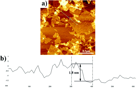 |
| | Fig. 1 AFM image of the GO sheets deposited on the mica substrates: (a) the surface morphology of GO sheets. (b) The height profile of GO sheets along the white line shown in (a). | |
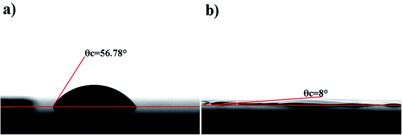
The substrate PET was put under the nozzle at a distance of 1 mm, and its surface energy influenced the morphology and resolution of the printed patterns.31 To match the surface energy of the substrate with that of the ink, improving the wetting and spreading of the ink on PET, oxygen-plasma treatment was carried out to make PET hydrophilic. Comparison of the contact angles of the ink on the untreated (Fig. 2a) and treated substrates (Fig. 2b) showed that the contact angle decreased from 56.78° to 8°, and the surface energy calculated from the Owens equation in two liquids32 increased from 42.52 mJ m−2 to 57.75 mJ m−2; this proved the wetting behavior of the ink on the substrate.
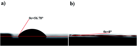 |
| | Fig. 2 The contact angle of the GO ink on different substrates: (a) untreated PET and (b) treated PET. | |
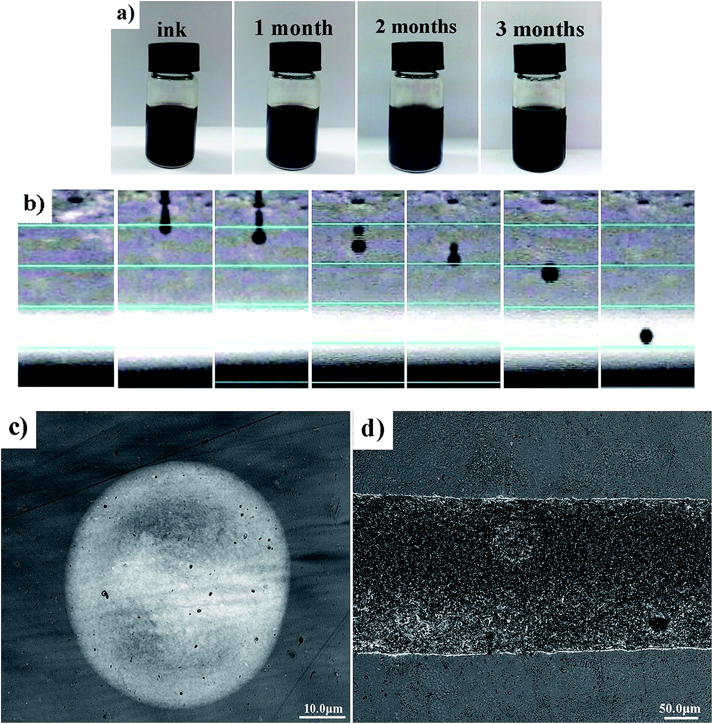
The prepared printable ink can remain stable for up to three months and have no aggregation, as shown in Fig. 3a. A droplet was injected from the nozzle successfully, separated into two drops, and finally merged into a single drop before exposing the treated PET (Fig. 3b); moreover, a satellite drop was not generated. There was almost no coffee ring observed in the printed single drop, as shown in Fig. 3c, and the line had flat edges and high resolution (Fig. 3d), with GO sheets distributed uniformly within its inner side.
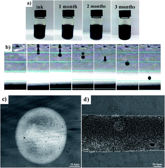 |
| | Fig. 3 Schematic of ink and printing: (a) stability of the prepared ink changing with time (just-prepared; one month; two months; and three months); (b) the injecting procedure of the ink from nozzles; (c) the morphology of a printed single drop; and (d) the morphology of a printed line. | |
3.2 Morphology and conductivity of the printed patterns
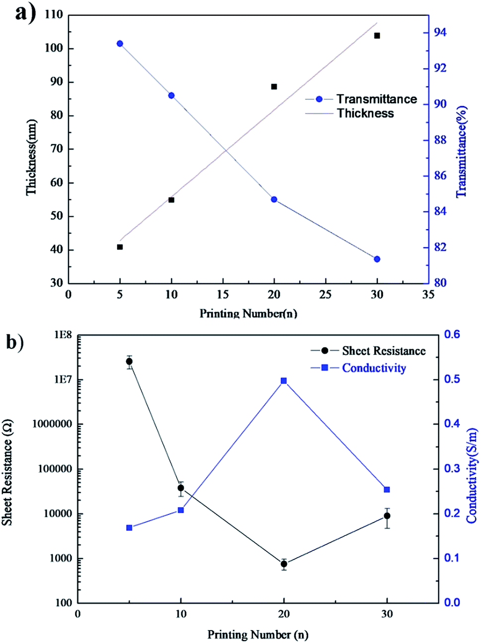
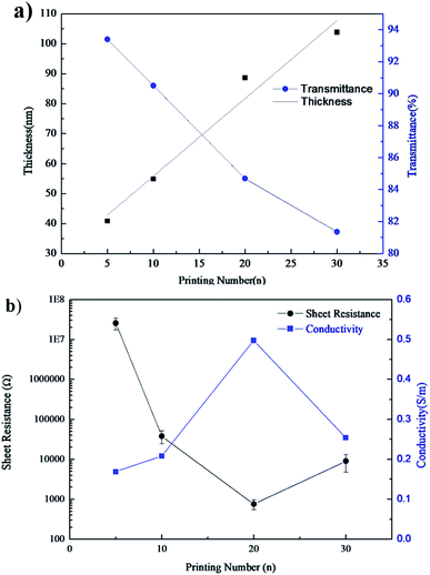
The number of printing passes directly influenced the thickness of the printed patterns.10 The thickness of the printed patterns scaled linearly with the printing times, as shown in Fig. 4. After printing 5 and 30 passes, the thickness of the printed patterns was 40.81 nm and 113.83 nm, respectively, with each additional printing pass adding 5 nm thickness prior to IPL reduction. The transmittance of the printed patterns decreased from 93.4% to 81.4% as the passes increased from 5 to 30, respectively. As expected, the resistance decreased as the printing passes increased from 5 passes to 20 passes, corresponding to the conductivity increase, as shown in Fig. 4b. When 20 passes were printed, the resistance of the pattern was 56.77 MΩ, and the conductivity of the pattern was 0.497 S m−1. It achieved the best conductivity among the experimentally printed patterns. The conductivity of the 30-pass printed pattern decreased as compared to that of the 20-pass printed pattern. This was caused by more solvents in the patterns that affected the contact between GO sheets.
 |
| | Fig. 4 Relationships between: (a) thickness and the transmittance and (b) the sheet resistance and the conductivity of the printed patterns and the printing numbers. | |
The morphology of the printed patterns is indicated in the SEM images (Fig. 5) and the AFM images (Fig. 6). Notably, there were many ridges and flat regions in the patterns (Fig. 5). Morphologies of the ridges and flat regions are shown in Fig. 6a and b, respectively. As shown in Fig. 6a, the height of the ridges was nearly 260 nm, much larger than the thickness of GO as well as smaller than the lateral dimension of GO. As shown in Fig. 6b, the roughness of the flat region in the printed patterns was smaller than the roughness of the substrate PET; thus, it could be judged that there were still GO sheets on the flat basal plane. The ridges were produced because when GO inks were exposed to the substrate, the solvents inside the patterns evaporated. During this process, GO sheets were carried with solvents and moved. When the moving GO sheets collided with each other, ridges were formed.33,34
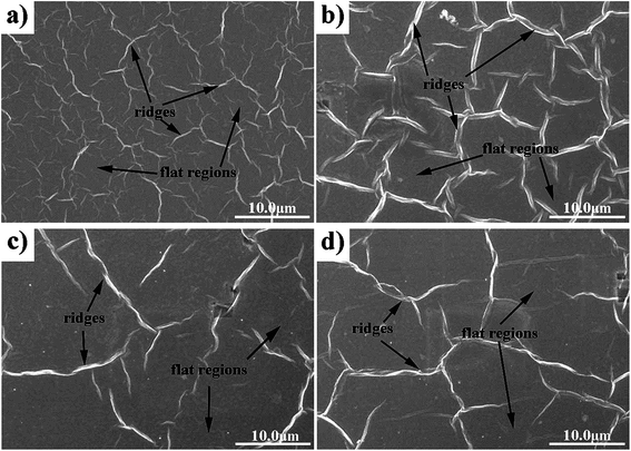 |
| | Fig. 5 SEM images of the films before IPL reduction with different printed passes on PET using GO ink: (a), (b), (c), and (d) corresponding to 5, 10, 20, and 30 times, respectively. | |
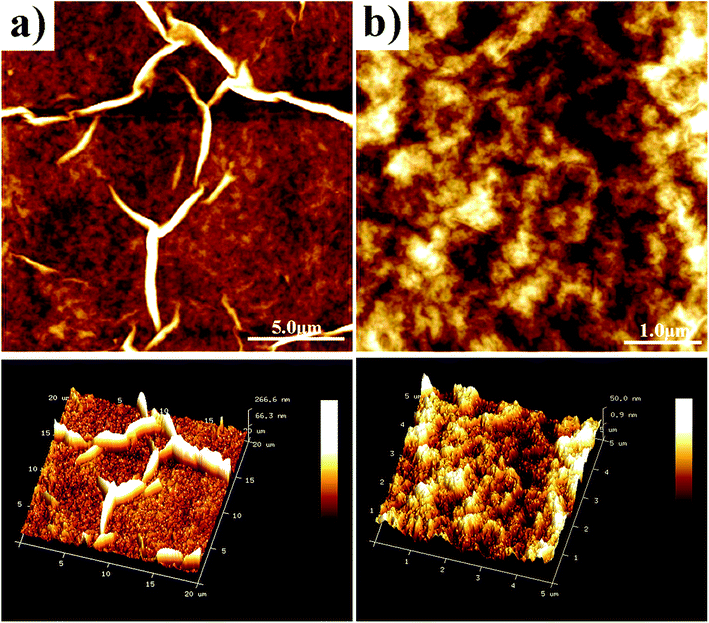 |
| | Fig. 6 AFM morphology and 3D profile images of the patterns printed using the GO ink (20 printing passes): (a) morphology of the ridges and (b) morphology of the flat regions. | |
3.3 Reduction of the printed patterns using IPL
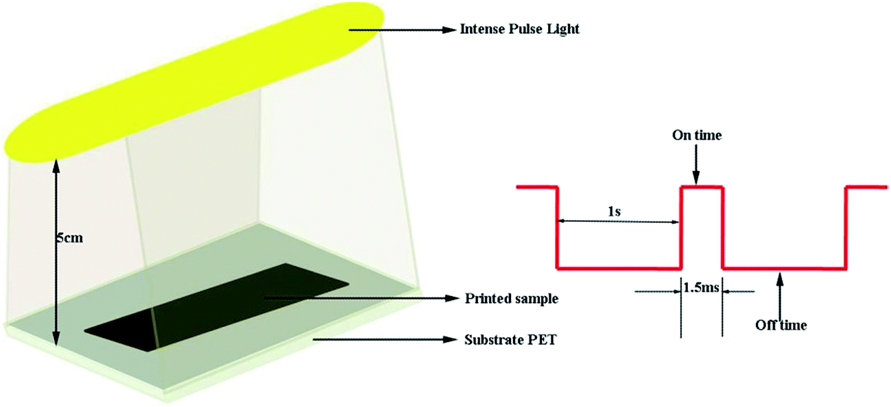
Reduction of the printed GO patterns was performed by photonic sintering. The xenon lamp emits a broad emission spectrum ranging from 190 nm to 800 nm. Fig. 7 shows a schematic of the IPL reduction treatment under the atmospheric environment at room temperature. The distance between the xenon lamp and the samples was set at 5 cm, and the patterns were treated under a single pulse for the time duration of 1.5 ms.
 |
| | Fig. 7 Schematic of the IPL treatments. | |
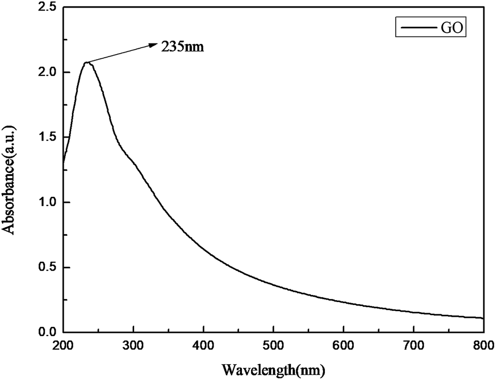
Short-pulse bursts of high energy will generate a much higher heating rate and higher transient temperature. During the IPL irradiation, intensive light was delivered onto the printed GO films within a few milliseconds. The temperature of the films became high instantly because of the photo-thermal effect, which could break the bonds in the structure of GO sheets and lead to the reduction of the GO films. Moreover, the spectrum range of the xenon lamp matches well with that of the maximum resonance absorption peak of the GO sheets at 235 nm, as shown in Fig. 8. As a result, the bonds in the GO sheets generated resonation with light in typical spectrum ranges; this accelerated the removal of oxygen functional groups and restoration of the original structure of graphene.
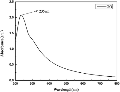 |
| | Fig. 8 Absorption spectrum of the GO sheets. | |
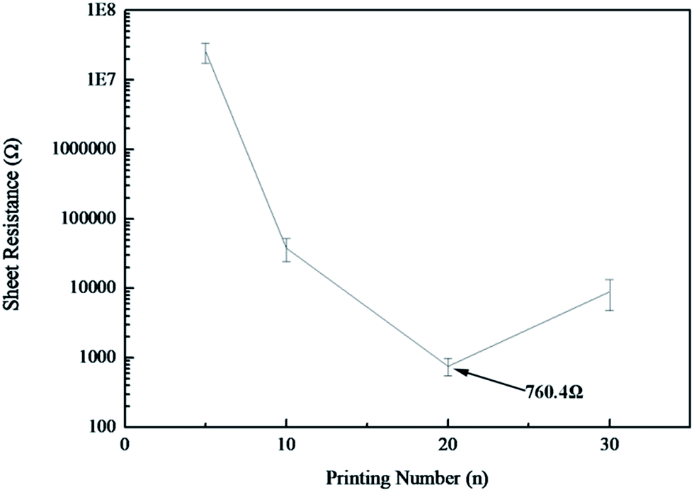
Compared with the patterns obtained before IPL, patterns treated with IPL exhibited fewer ridges, darker colors, and cracks (Fig. 9). The ridges became fewer and fewer as the number of printing passes increased. The number of cracks increased as the printing passes increased. After reduction, the patterns printed for 30 passes cracked completely and had weaker binding force with the substrate. It was seen that the conductivity of the patterns after reduction improved largely; especially, the resistance of the sample with 20 printing passes decreased to around 760.4 Ω, four orders of magnitude less than that of the patterns without reduction (Fig. 10). In their reported study, Zhao30 et al. reduced thin GO films using HI acid, and the RGO films showed a sheet resistance of 840 Ω. Kong35 et al. developed a flexible electrode with a sheet resistance of 0.3 MΩ by reducing a GO electrode with an infrared heat lamp at a temperature of 200 °C. Compared with the abovementioned reports, the 20 printing-passes pattern after IPL treatment exhibited superior conductivity in this study. When the printed patterns were placed under light, GO sheets were reduced by the instantaneous high temperature, and the solvent evaporated rapidly. Thus, the conductivity of the patterns after IPL improved. On the other hand, solvents tended to escape from regions with ridges. This caused cracks and reduced the number of ridges on the pattern surface. Although there were more cracks on the pattern surface, the resistance of the pattern with 20 passes after IPL treatment was lower than that of the patterns with 5 and 10 passes. It was mainly because more reduced GO sheets in the pattern with 20 passes resulted in more inter-flake junctions between reduced GO sheets as the printing passes increased. It led to the formation of more conduction pathways for electrons to immigrate and the improvement of the pattern resistance. Moreover, the volume of solvents inside the patterns increased with the increasing printing passes. It caused more solvent escaping, and thus, more cracks occurred. Therefore, compared with that of the pattern with 20 passes, the higher resistance of the 30 printing-passes pattern was attributed to too many cracks on its surface that seriously impeded the reduced GO sheets contact.
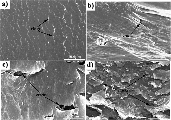 |
| | Fig. 9 SEM images of films after IPL reduction with different printed passes on PET using GO ink: (a), (b), (c), and (d) corresponding to 5, 10, 20, and 30 times, respectively. | |
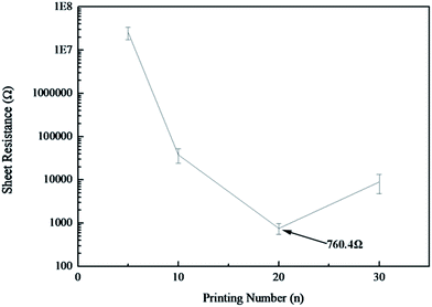 |
| | Fig. 10 Relationship between the printing numbers and the resistance after IPL reduction. | |
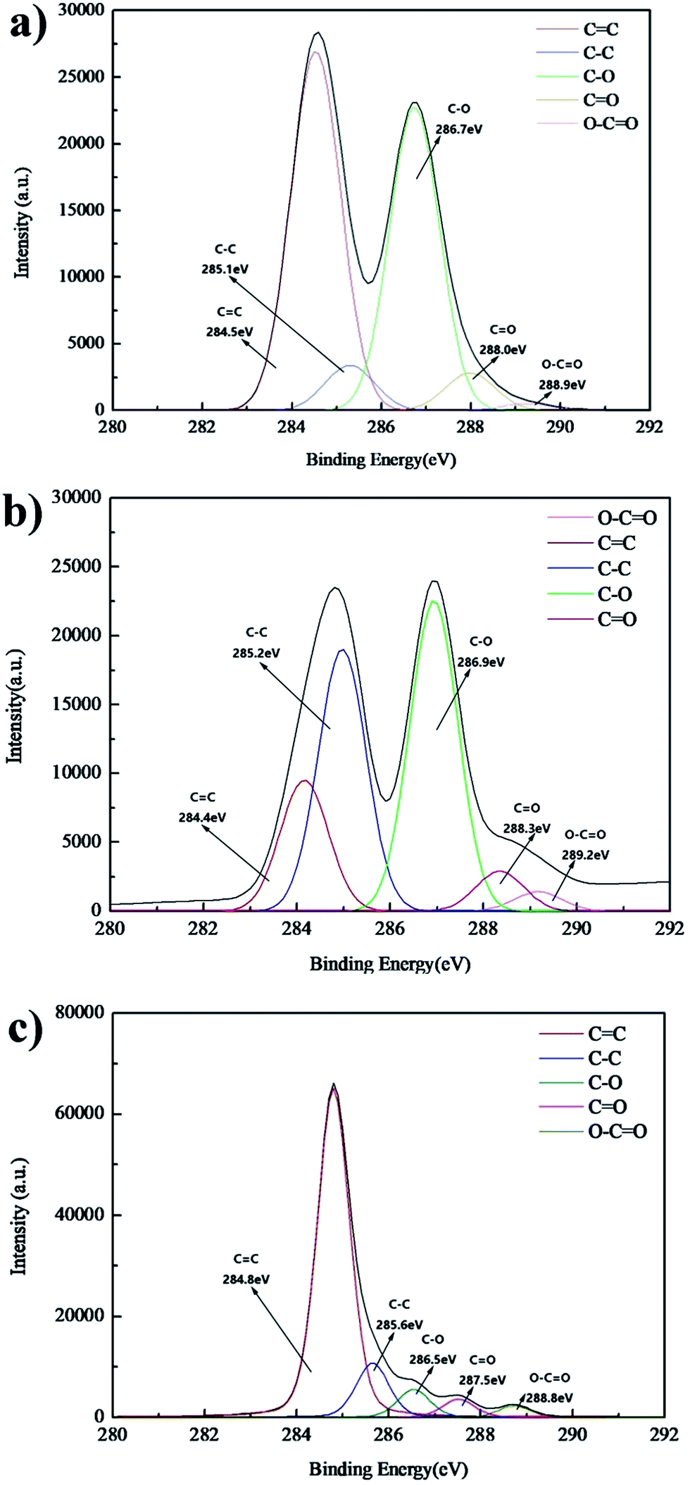
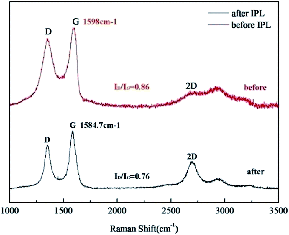
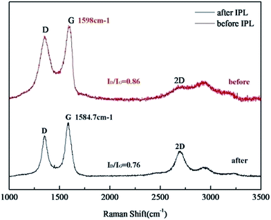
To confirm the effectiveness of the GO reduction by IPL, XPS spectra of the GO powder and printed samples before and after reduction were compared. The XPS C 1s spectra for all samples indicated typical characteristics of graphene materials. The dominant peak around 284.5 eV was ascribed to the region of C![[double bond, length as m-dash]](https://www.rsc.org/images/entities/char_e001.gif) C, the peak around 285.3 eV was ascribed to the region of C–C, the peak between 286.5 eV and 287.5 eV is within the carbon region of C–O and CO, and the peak around 289.0 eV is the signal of carboxyl carbon.29,36 Interestingly, it was seen that as compared to that in the GO powder (Fig. 11a), the percentage of C–C bonding and C–O bonding in the printed patterns before reduction became larger, respectively increasing from 30.18% and 38.33% to 34.01% and 40.91%, due to carbon–oxygen bonding of the solvents. Compared with the printed patterns before reduction, the percentage of CC/C–C bonding in patterns after IPL was significantly enhanced from the original 50.66% to 86.88%, even higher than that of the GO powder (54.30%). Moreover, the percentage of C–O decreased from 40.91% for the patterns before reduction to 6.41% after reduction. It proved that the π-conjugated structure of graphene was restored, and the solvents in the samples evaporated; this increased the electrical conductivity of the patterns after IPL.37,38 In the Raman spectra (Fig. 12), patterns after IPL had a lower ratio for the intensity of the D band to that of the G band (ID/IG) than patterns before IPL, and the G band in the patterns after IPL downshifted from 1598 cm−1 for the patterns before IPL to around 1584.7 cm−1; this indicated that the conjugated structure was restored, and the defect density in the carbon basal plane was lower, closer to that of pristine graphene.39,40
C, the peak around 285.3 eV was ascribed to the region of C–C, the peak between 286.5 eV and 287.5 eV is within the carbon region of C–O and CO, and the peak around 289.0 eV is the signal of carboxyl carbon.29,36 Interestingly, it was seen that as compared to that in the GO powder (Fig. 11a), the percentage of C–C bonding and C–O bonding in the printed patterns before reduction became larger, respectively increasing from 30.18% and 38.33% to 34.01% and 40.91%, due to carbon–oxygen bonding of the solvents. Compared with the printed patterns before reduction, the percentage of CC/C–C bonding in patterns after IPL was significantly enhanced from the original 50.66% to 86.88%, even higher than that of the GO powder (54.30%). Moreover, the percentage of C–O decreased from 40.91% for the patterns before reduction to 6.41% after reduction. It proved that the π-conjugated structure of graphene was restored, and the solvents in the samples evaporated; this increased the electrical conductivity of the patterns after IPL.37,38 In the Raman spectra (Fig. 12), patterns after IPL had a lower ratio for the intensity of the D band to that of the G band (ID/IG) than patterns before IPL, and the G band in the patterns after IPL downshifted from 1598 cm−1 for the patterns before IPL to around 1584.7 cm−1; this indicated that the conjugated structure was restored, and the defect density in the carbon basal plane was lower, closer to that of pristine graphene.39,40
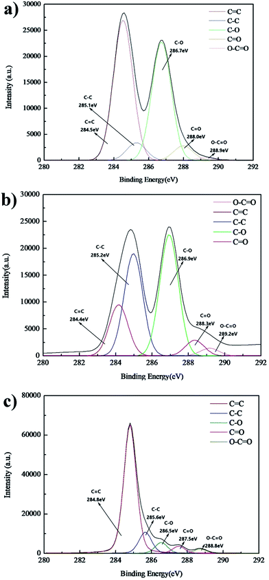 |
| | Fig. 11 XPS spectra of (a) GO powders; (b) GO printed patterns (20 passes) before IPL; (c) GO printed patterns (20 passes) after IPL. | |
 |
| | Fig. 12 Raman spectra of the patterns (20 passes) before and after IPL reduction. | |
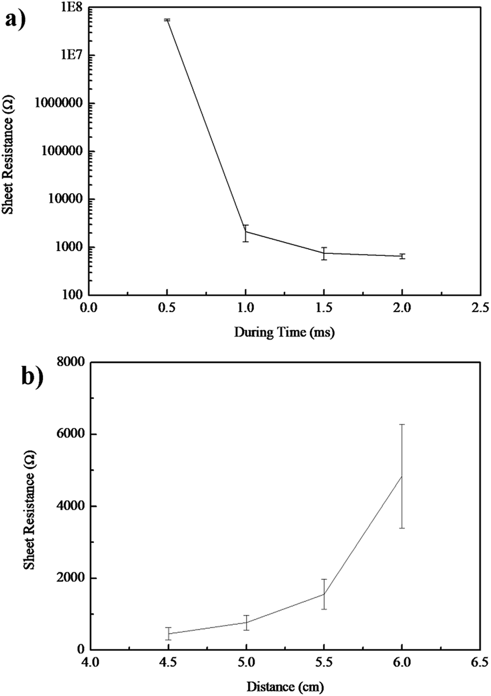
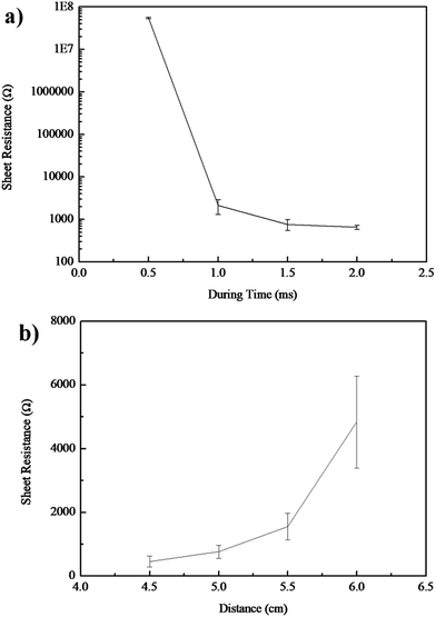
To explore optimized reduction parameters, the distance between the light and the samples and time duration of the pulses were changed, and their effects on the conductivity and morphology of the patterns were investigated.28 As shown in Fig. 13, resistance of the patterns after IPL decreased with the increasing pulse duration time or decreasing distance, and it achieved the highest value when the distance was increased to 4.5 cm or the duration time was up to 2.0 ms. However, binding force between the patterns and the substrate was too low to keep the patterns adhered to the substrate; thus, the optimized parameters were set as 1.5 ms and 5.5 cm.
 |
| | Fig. 13 Relationship between resistance and (a) during time of the pulse; (b) distance between patterns and light. | |
3.4 Flexibility of the reduced patterns
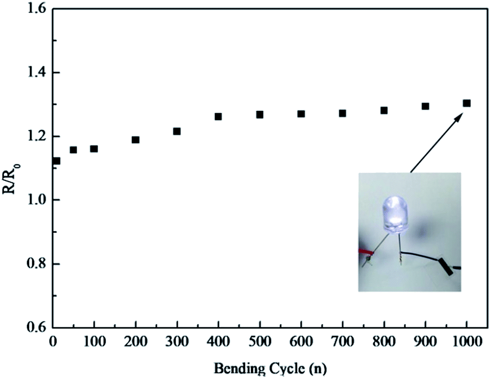
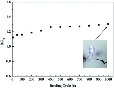
Resistances of the printed patterns on PET under different bending cycles were measured (Fig. 14) to reveal the flexibility of the printed patterns after IPL. When the 20 passes-printed patterns were bent outwards by 180° after 1000 bending cycles, there were no observable cracks on the plane, and the patterns became levelled again. The change of resistance was still acceptable. This result indicates that inkjet printing of the GO ink can generate flexible patterns that satisfy the requirements of flexible devices.
 |
| | Fig. 14 Resistance measured as a function of bending cycles for GO patterns on PET after IPL reduction. | |
4. Conclusions
In summary, a printable GO ink was successfully prepared in solvents involving deionized water, ethylene glycol, and ethanol. Patterns with a high resolution were inkjet-printed with the prepared inks. Printed GO patterns were reduced rapidly with IPL treatment to achieve low resistance and fine morphology. Upon printing 20 passes, the resistance achieved was as low as 760.4 Ω after IPL reduction. Compared with the resistance of the patterns before IPL treatment, the resistance of the patterns after IPL was lowered by nearly four orders of magnitude. Moreover, after bending outwards 180° for 1000 cycles, the resistance of the reduced GO patterns changed slightly, and this was still acceptable. Furthermore, the substrate PET, sensitive to high temperatures, was unbroken after IPL. This establishes that GO ink can be reduced by the IPL method, and this result can be used as a reference for flexible, printed electronics such as sensors and electrodes.
Conflicts of interest
There are no conflicts to declare.
References
- T. Felice, H. Tawfique, W. Weiping, S. Zhipei, L. Antonio, S. K. Tero, H. Gen-Wen, J. Sungjune, B. Francesco, J. P. Philip, C. Daping and C. F. Andrea, ACS Nano, 2012, 6(4), 2992–3006 CrossRef PubMed.
- M. H. Ervin, L. T. Le and W. Y. Lee, Electrochim. Acta, 2014, 147, 610–616 CrossRef CAS.
- J. Viventi, D. H. Kim, L. Vigeland, E. S. Frechette, J. A. Blanco, Y. S. Kim, A. E. Avrin, V. R. Tiruvadi, S. W. Hwang, A. C. Vanleer, D. F. Wulsin, K. Davis, C. E. Gelber, L. Palmer, J. Van der Spiegel, J. Wu, J. Xiao, Y. Huang, D. Contreras, J. A. Rogers and B. Litt, Nat. Neurosci., 2011, 14, 1599–1605 CrossRef CAS PubMed.
- D. Tobjork and R. Osterbacka, Adv. Mater., 2011, 23, 1935–1961 CrossRef PubMed.
- L. F. Lima, C. F. Matos, L. C. Gonçalves, R. V. Salvatierra, C. E. Cava, A. J. G. Zarbin and L. S. Roman, J. Phys. D: Appl. Phys., 2016, 49, 105106 CrossRef.
- T. Vuorinen, M. Zakrzewski, S. Rajala, D. Lupo, J. Vanhala, K. Palovuori and S. Tuukkanen, Adv. Funct. Mater., 2014, 24, 6340–6347 CrossRef CAS.
- X. Huang, T. Leng, M. Zhu, X. Zhang, J. Chen, K. Chang, M. Aqeeli, A. K. Geim, K. S. Novoselov and Z. Hu, Sci. Rep., 2015, 5, 18298 CrossRef CAS PubMed.
- S. Wünscher, R. Abbel, J. Perelaer and U. S. Schubert, J. Mater. Chem. C, 2014, 2, 10232–10261 RSC.
- H. Zhang, A. Xie, Y. Shen, L. Qiu and X. Tian, Phys. Chem. Chem. Phys., 2012, 14, 12757–12763 RSC.
- K. Y. Shin, J. Y. Hong and J. Jang, Adv. Mater., 2011, 23, 2113–2118 CrossRef CAS PubMed.
- B. Zhan, C. Li, J. Yang, G. Jenkins, W. Huang and X. Dong, Small, 2014, 10, 4042–4065 CrossRef CAS PubMed.
- W. Shen, X. Zhang, Q. Huang, Q. Xu and W. Song, Nanoscale, 2014, 6, 1622–1628 RSC.
- Y. Gao, W. Shi, W. Wang, Y. Leng and Y. Zhao, Ind. Eng. Chem. Res., 2014, 53, 16777–16784 CrossRef CAS.
- E. B. Secor, P. L. Prabhumirashi, K. Puntambekar, M. L. Geier and M. C. Hersam, J. Phys. Chem. Lett., 2013, 4, 1347–1351 CrossRef CAS PubMed.
- J. Li, F. Ye, S. Vaziri, M. Muhammed, M. C. Lemme and M. Ostling, Adv. Mater., 2013, 25, 3985–3992 CrossRef CAS PubMed.
- V. Dua, S. P. Surwade, S. Ammu, S. R. Agnihotra, S. Jain, K. E. Roberts, S. Park, R. S. Ruoff and S. K. Manohar, Angew. Chem., 2010, 49, 2154–2157 CrossRef CAS PubMed.
- K. S. Novoselov, V. I. Fal'ko, L. Colombo, P. R. Gellert, M. G. Schwab and K. Kim, Nature, 2012, 490, 192–200 CrossRef CAS PubMed.
- C.-L. Lee, C.-H. Chen and C.-W. Chen, Chem. Eng. J., 2013, 230, 296–302 CrossRef CAS.
- T. Le, V. Lakafosis, T. Thai, Z. Y. Lin and M. Tentzeris, 2012 International Conference on Electromagnetics In Advanced Applications (Iceaa), 2012, pp. 954–957 Search PubMed.
- Y. Su, S. Jia, J. Du, J. Yuan, C. Liu, W. Ren and H. Cheng, Nano Res., 2015, 8, 3954–3962 CrossRef CAS.
- L. Huang, Y. Huang, J. Liang, X. Wan and Y. Chen, Nano Res., 2011, 4, 675–684 CrossRef CAS.
- A. Kamyshny and S. Magdassi, Small, 2014, 10, 3515–3535 CrossRef CAS PubMed.
- L. T. Le, M. H. Ervin, H. Qiu, B. E. Fuchs and W. Y. Lee, Electrochem. Commun., 2011, 13, 355–358 CrossRef CAS.
- K. Chi, Z. Zhang, J. Xi, Y. Huang, F. Xiao, S. Wang and Y. Liu, ACS Appl. Mater. Interfaces, 2014, 6, 16312–16319 CAS.
- F. Xiao, S. Yang, Z. Zhang, H. Liu, J. Xiao, L. Wan, J. Luo, S. Wang and Y. Liu, Sci. Rep., 2015, 5, 9359 CrossRef CAS PubMed.
- S. Das, D. Cormier and S. Williams, Procedia Manufacturing, 2015, 1, 366–377 CrossRef.
- J. S. Kang, J. Ryu, H. S. Kim and H. T. Hahn, J. Electron. Mater., 2011, 40, 2268–2277 CrossRef CAS.
- E. B. Secor, B. Y. Ahn, T. Z. Gao, J. A. Lewis and M. C. Hersam, Adv. Mater., 2015, 27, 6683–6688 CrossRef CAS PubMed.
- B. Derby, Annu. Rev. Mater. Res., 2010, 40, 395–414 CrossRef CAS.
- J. P. Zhao, S. F. Pei, W. C. Ren, L. B. Gao and H. M. Cheng, ACS Nano, 2010, 4, 5245–5252 CrossRef CAS PubMed.
- S. Santra, G. Hu, R. C. Howe, A. De Luca, S. Z. Ali, F. Udrea, J. W. Gardner, S. K. Ray, P. K. Guha and T. Hasan, Sci. Rep., 2015, 5, 17374 CrossRef CAS PubMed.
- H. Tavana, C. N. Lam, K. Grundke, P. Friedel, D. Y. Kwok, M. L. Hair and A. W. Neumann, J. Colloid Interface Sci., 2004, 279, 493–502 CrossRef CAS PubMed.
- M. Kuang, L. Wang and Y. Song, Adv. Mater., 2014, 26, 6950–6958 CrossRef CAS PubMed.
- H. Kim, J. I. Jang, H. H. Kim, G. W. Lee, J. A. Lim, J. T. Han and K. Cho, ACS Appl. Mater. Interfaces, 2016, 8, 3193–3199 CAS.
- D. Kong, L. T. Le, Y. Li, J. L. Zunino and W. Lee, Langmuir, 2012, 28, 13467–13472 CrossRef CAS PubMed.
- K. Y. Shin, J. Y. Hong and J. Jang, Chem. Commun., 2011, 47, 8527–8529 RSC.
- M. Bai, J. Chen, W. Wu, X. Zeng, J. Wang and H. Zou, Colloids Surf., A, 2016, 490, 59–66 CrossRef CAS.
- Y. Su, J. Du, D. Sun, C. Liu and H. Cheng, Nano Res., 2013, 6, 842–852 CrossRef CAS.
- H. A. Becerril, J. Mao, Z. Liu, R. M. Stoltenberg, Z. Bao and Y. Chen, ACS Nano, 2008, 2, 463–470 CrossRef CAS PubMed.
- A. C. Ferrari and D. M. Basko, Nat. Nanotechnol., 2013, 8, 235–246 CrossRef CAS PubMed.
|
| This journal is © The Royal Society of Chemistry 2017 |
Click here to see how this site uses Cookies. View our privacy policy here. 
 Open Access Article
 This Open Access Article is licensed under a Creative Commons Attribution-Non Commercial 3.0 Unported Licence
 *
*