
 Open Access Article
 This Open Access Article is licensed under a
 Creative Commons Attribution 3.0 Unported Licence
Toward fast growth of large area high quality graphene using a cold-wall CVD reactor
Aaesha Alnuaimi *,
Ibraheem Almansouri,
Irfan Saadat and
Ammar Nayfeh
*,
Ibraheem Almansouri,
Irfan Saadat and
Ammar Nayfeh
Department of Electrical and Computer Engineering (ECE), Masdar Institute, Khalifa University of Science and Technology, P.O. Box 54224, Abu Dhabi, United Arab Emirates. E-mail: aar.alnuaimi@gmail.com
First published on 8th November 2017
Abstract
In this work we provide a detailed analysis on graphene synthesis by Chemical Vapor Deposition (CVD) using a cold wall CVD reactor to achieve fast production of large area high quality graphene. Using Raman spectroscopy and mapping, the effect of growth temperature, pressure and CH4![[thin space (1/6-em)]](https://www.rsc.org/images/entities/char_2009.gif) :H2 ratio have been analyzed. The results show that graphene synthesis at high temperature results in reducing the multilayer nucleation density. At a high temperature of 1060 °C, the density of multilayer graphene was reduced by more than 50%. In addition, our analysis revealed that the chamber pressure plays a major role in reducing the multilayer region formation and controlling the grain size of graphene. At 15 mbar, high quality graphene with a large grain size greater than 5 μm is achieved. Moreover, the hydrogen to methane ratio has a significant role in determining the morphology and the size of graphene domains. Our analysis provide guidelines toward the synthesis of high quality graphene using 4′′ cold wall CVD reactor that are beneficial for the large scale production of graphene.
:H2 ratio have been analyzed. The results show that graphene synthesis at high temperature results in reducing the multilayer nucleation density. At a high temperature of 1060 °C, the density of multilayer graphene was reduced by more than 50%. In addition, our analysis revealed that the chamber pressure plays a major role in reducing the multilayer region formation and controlling the grain size of graphene. At 15 mbar, high quality graphene with a large grain size greater than 5 μm is achieved. Moreover, the hydrogen to methane ratio has a significant role in determining the morphology and the size of graphene domains. Our analysis provide guidelines toward the synthesis of high quality graphene using 4′′ cold wall CVD reactor that are beneficial for the large scale production of graphene.
1. Introduction
Since the discovery of graphene by Novoselov et al. in 2004,1 graphene has attracted world-wide attention due to its remarkable mechanical, optical and electrical properties. Graphene is a two-dimensional material consisting of carbon atoms arranged in a planar hexagonal configuration. The first production of graphene was through mechanical exfoliation from graphite flakes. However, this method prevented its usage on a large-scale since the size of the exfoliated graphene was limited to hundreds of microns thus efforts have been dedicated to produce graphene on a large scale. Several methods have been developed to produce graphene including top down approaches such as mechanical exfoliation and chemical exfoliation and bottom up approaches such as epitaxial growth of graphene on SiC surfaces,2–4 reduction of graphene oxide5,6 and Chemical Vapor Deposition (CVD).7–9CVD is considered the most promising method to produce large area and continuous graphene films with good optical and electrical properties. During the CVD growth of graphene, the hydrocarbon precursor is decomposed thermally on a heated substrate to produce graphene. The most commonly used catalysts in CVD growth of graphene are transition metals such as nickel (Ni) and copper (Cu).7–9 Ni catalysts usually produce multilayer graphene due to their high carbon solubility. The growth of graphene using Cu catalysts was first demonstrated by Li et al.10 where graphene was synthesized on Cu foil using a mixture of methane and hydrogen at 1000 °C under low pressure condition using quartz tube reactor. The low solubility of carbon in copper foil and poor carbon saturation as a result of graphene surface coverage resulted in forming a single monolayer graphene with a coverage of more than 95%.10 Since then, research has been carried out to further enhance the monolayer coverage and increase the graphene domain size to obtain graphene with better electrical and optical properties that is beneficial for its application in electronics and optoelectronics devices.
Graphene grown using CVD is typically polycrystalline with a grain size of around 10 μm.11 The quality and the uniformity of graphene is strongly dependent on the deposition conditions. Most of the work reported in literature is done using home-made quartz tube hot wall CVD systems. Such home-made hot wall CVD systems differ in their configuration which adds a great amount of variability to graphene synthesis and make the parameters transfer process from one system to another challenging.11 In addition, hot-wall CVD reactors require long ramping-up and cooling-down procedures which are time consuming and limit the throughput for industrial scale synthesis of graphene.12,13 Cold wall CVD reactors are considered as an attractive option for large scale production of graphene with high throughput and thus reduced production cost.12–14 Cold wall CVD reactor has several advantages over hot wall CVD reactors including rapid sample heating and cooling time which is beneficial for achieving fast growth. In addition, the reduced gas phase chemical reaction in cold-wall CVD reactors contributed to better control of the film quality. Furthermore, cold-wall CVD reactor has lower heat capacity since it requires a local heater adjacent to the sample and therefore, cold-wall CVD reactor consumes less power.12–14 Thus, cold wall CVD reactor provides fast growth with better control of the film quality and less power consumption. There are several types of cold wall CVD reactors that differ depending on the heating source such as magnetic induction heating CVD,15 resistively heated stage CVD,12,16 joule heating induced CVD17,18 and Rapid Thermal Annealing CVD using halogen lamp heating.19,20
Several studies have reported the growth of high quality monolayer graphene using the different cold wall CVD reactors. Miseikis et al.11 studied the growth of graphene using cold wall CVD reactor that is based on using graphite heater. In their study, they have shown that graphene domain size, morphology and density are affected by the annealing conditions of Cu foil prior the growth step. It was suggested that the combination of oxygen passivated Cu foil with Argon (Ar) annealing yields the lowest nucleation density and the largest graphene domains. In addition, they have shown that sample enclosure helps in increasing the size of graphene domain and by further investigating the growth inside Cu pocket, they have shown that 1–3 mm domain size is achievable. Using the same cold wall CVD reactor based on graphite heater, Tao et al.21 investigated the growth of graphene on evaporated copper film <111> on silicon oxide on silicon SiO2/Si substrate. They have demonstrated that high quality graphene can be grown on hydrogen enriched copper at temperature <900 °C under hydrogen free methane precursor. In their study, Toe et al. demonstrated that graphene grains commensurate the grains of the underlying copper film suggesting that controlling the size of the graphene grains can be achieved by controlling the size and the crystal orientation of the underlying copper film. This observation highlights the difference between the use of copper foil and evaporated copper film since graphene domains grown on copper foil mostly traverse the grain boundaries of the underlying copper foil. Liu et al.22 focused mainly on the effect of copper pre-treatment, purity and hydrocarbon gas concentration on the synthesis of graphene using Aixtron cold wall CVD reactor.
Das et al.,14 have studied the nucleation density and size of graphene domains using a home-made cold wall CVD reactor under flow of hydrogen (H2), argon (Ar) and methane (CH4). Their study focused on the effect of gases ratio on the nucleation density and the size of graphene domains. Bointon et al.12 studied graphene synthesis using resistive heating cold wall CVD reactor. It has been shown that graphene grown using this type of reactor adapts a different growth mechanism from that of the hot-wall CVD reactor. Bointon et al. have shown that graphene forms a thick carbon layer of approximately (100 nm) thickness in the early stages of the growth. The thickness of this layer is reduced with time to form graphene islands. Moreover, the time for the layer to form graphene islands is temperature dependent. By increasing the growth time, the graphene islands merge to form continues graphene layer.
Mu et al.13 analyzed the synthesis of bi-layer graphene using cold-wall CVD reactor. It has been shown that long growth time would result in forming bilayers graphene. Higher hydrogen flow rate increase the time required to form the bilayers. At very high hydrogen rate, there was no visible bilayer formation confirming that high hydrogen hinders the bilayers growth. Their observation on the role of hydrogen during the growth of bilayers graphene suggest that hydrogen deactivate the nucleation site of bilayer graphene at the early stage and depresses the growth speed of both monolayer and bilayer graphene during the full growth process. Mu et al. reported that the role of hydrogen in bilayer formation is contradictory to that for synthesis in the tubular hot wall quartz CVD furnace since in such system, the hydrogen passivates the edge of the top layer graphene and allows active carbon atoms to diffuse into the area underneath the top graphene to form ad layer underneath.
Despite all the efforts on graphene synthesis using cold wall CVD reactor, there is still lack of comprehensive analysis on the effect of growth parameters for fast and large scale production of high quality graphene using this configuration. Herein we analyzed the effect of growth temperature, chamber pressure andCH4:H2 ratio on the synthesis of graphene using Aixtron black magic Pro 4-inch reactor to produce high quality monolayer graphene on 4-inch Cu foil to achieve fast growth of high quality graphene.
2. Experimental methods
2.1 Graphene synthesis in a cold wall CVD reactor
Graphene was grown using 4-inch cold wall Aixtron BM CVD system. The CVD reactor consists of top and bottom graphite heater to ensure that the temperature is distributed uniformly over the growth region. The growth was done under mixture of H2 and CH4 gases. The foil used in the synthesis is 35 μm thick electro-polished with purity of 99.8% (advent research materials). The graphene growth was done in four main steps as demonstrated in Fig. 1.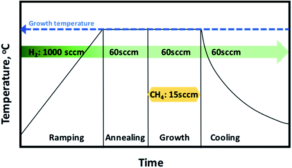 | ||
| Fig. 1 Steps involved during graphene growth using CVD. | ||
The first step involves ramping up the temperature. The temperature was increased to the desired growth temperature with ramping rate of 75 °C per minute under flow of 1000 sccm H2. The second step involves annealing the copper foil prior to the graphene growth under flow of H2 for 10 min. The annealing step is considered a critical step in graphene growth as it helps in increasing the copper grain size, smoothening the Cu surface and removing the residual copper oxide from the surface. The third step is graphene growth. In this step, the methane gas was introduced to the chamber in addition to H2. The methane flow was set to 15 sccm and hydrogen was set to 60 sccm. The growth time was kept to 10 min. The last step is the cooling down of the chamber under H2 flow to a temperature of 150 °C before the sample is exposed to air. Several experiments have been done to analyze the effect of growth temperature, pressure and CH4:H2 ratio.
2.2 Graphene transfer process and characterization
After each growth process the graphene was transferred to SiO2/Si substrate. The SiO2 was grown on Si using oxford Plasma Enhanced Chemical Vapour Deposition system (PECVD) with thickness of 300 nm. The graphene transfer process involves spin coating polymethyl methacrylate (492 PMMA A2) resists at speed of 1000 rpm for 1 min. The samples were baked at 180 °C for 1 min. Graphene grown on the backside of the copper foil was removed using Reactive Ion Etching (RIE) for 1 min. Ammonium persulfate (Sigma Aldrich) was used to etch the Cu. The PMMA/graphene floating membrane was rinsed with deionized water three times prior the transfer to SiO2/Si substrate to remove any residue of the etchant. The samples were immersed in acetone for 2 hours to remove PMMA. Raman analysis was performed using Witec alpha300 to check the quality and the uniformity of the monolayer graphene. The Raman mapping was done on 25 × 25 μm2 area using 488 nm blue laser and 100× objector. Scanning Electron Microscopy (SEM) using quanta 250 was used for the analysis of graphene domain shape and size.3. Results and discussion
3.1 Effect of growth temperature
As a first step in the optimization, the effect of growth temperature has been analyzed. The growth temperature was varied from 1000 °C to 1060 °C with an interval of 20 °C. Temperature above 1060 °C was not considered in the synthesis since it is close to the melting point of Cu foil which is approximately 1080 °C. The chamber pressure was fixed to 25 mbar. The Raman map of 2D band (2682 cm−1) intensity (I2D) to G band intensity (IG) (1580 cm−1) ratio (I2D/IG) for each temperature is shown in Fig. 2(a–d). For a monolayer graphene, the ratio of I2D/IG should be >2.23 As shown in Fig. 2(a–d), non-uniform thickness was observed with temperature. Graphene synthesized at 1000 °C results in forming multilayer graphene with a monolayer background. However, the density of the multilayer regions is reduced at higher temperature. As shown in Fig. 2(d), at 1060 °C there is a reduction in the multilayer regions by more than 50% compared to graphene deposition at 1000 °C. The Raman spectrum at different location of Raman map of I2D/IG intensity for graphene grown at 1060 °C is shown in Fig. 2(e).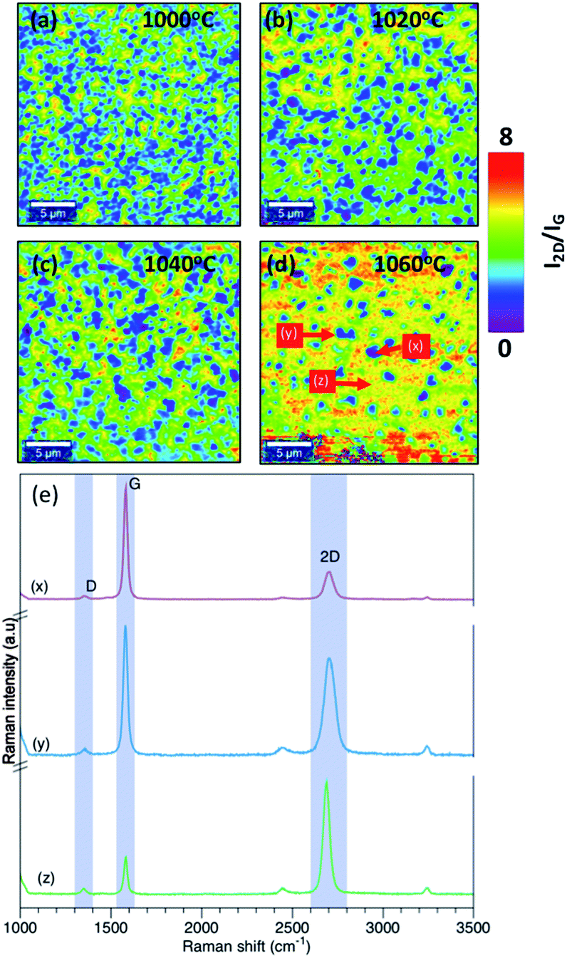 | ||
| Fig. 2 Raman map of I2D/IG intensity at (a) 1000 °C, (b) 1020 °C, (c) 1040 °C, (d) 1060 °C. (e) Raman spectrum at different location of Raman map of I2D/IG intensity at 1060 °C. | ||
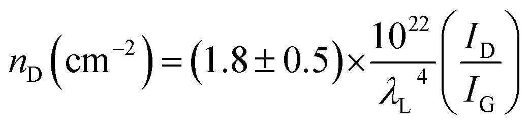
The existence of defects in graphene can be identified by the ratio of D band intensity (ID) (1350 cm−1) to G band intensity (ID). Low ID/IG intensity <0.5 suggests good quality graphene with less defects.23,24 This intensity ratio gives a good indication of the defect level in graphene. According to L. G. Cancado et al.24 the defect density can be estimated from ID/IG intensity ratio using eqn (1)
 | (1) |
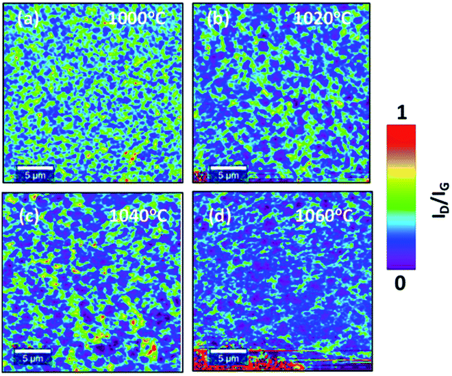 | ||
| Fig. 3 Raman map of ID/IG intensity at (a) 1000 °C, (b) 1020 °C, (c) 1040 °C, (d) 1060 °C. | ||
The above results suggest that graphene quality and thickness are highly affected by the growth temperature. Higher temperature results in reducing the graphene multilayer formation and improving the quality of the grown graphene. This is mainly attributed to an enhanced dissociation of carbon precursors at higher temperature as well as the formation of bigger copper grains that results in smoothening the surface. Several studies have also shown improvement in the graphene growth at higher temperature using quartz tube reactor. Xing et al.,25 attributed the temperature dependent graphene thickness to the difference in the amount of the consumed carbon concentration during the nucleation. At low temperatures, the amount of consumed carbon during the growth is higher compared to the amount consumed at higher temperatures which results in the formation of multilayer nucleation. According to Kim et al.,26 higher temperature leads to a lower density of nuclei with larger lateral size. In addition, Chen et al.,27 attributed the improvement in the graphene quality at higher temperatures to the enlargement in the catalyst grain size and the reduction in the density of the grain size of the catalyst.
3.2 Effect of chamber pressure
We further analyzed the effect of chamber pressure on the growth of graphene. The growth temperature was fixed to 1060 °C and the effect of chamber pressure was investigated at 25 mbar, 15 mbar and 5 mbar.Fig. 4(a–c) show the Raman map of I2D/IG intensity ratio at different chamber pressure. As demonstrated in Fig. 4(a–c), decreasing the chamber pressure from 25 mbar to 15 mbar and 5 mbar reduced the formation of multilayer graphene. Synthesized graphene at 15 mbar and 5 mbar revealed a uniform thickness of graphene with no observed multilayer regions. The observed small spots in the I2D/ID map is due to the PMMA residue. Additionally, the quality of graphene is enhanced with lower defect density as demonstrated in Fig. 4(d–f) which show the ID/IG intensity ratio. The corresponding Raman spectrum for graphene grown at different pressure is shown in figure Fig. 4(g).
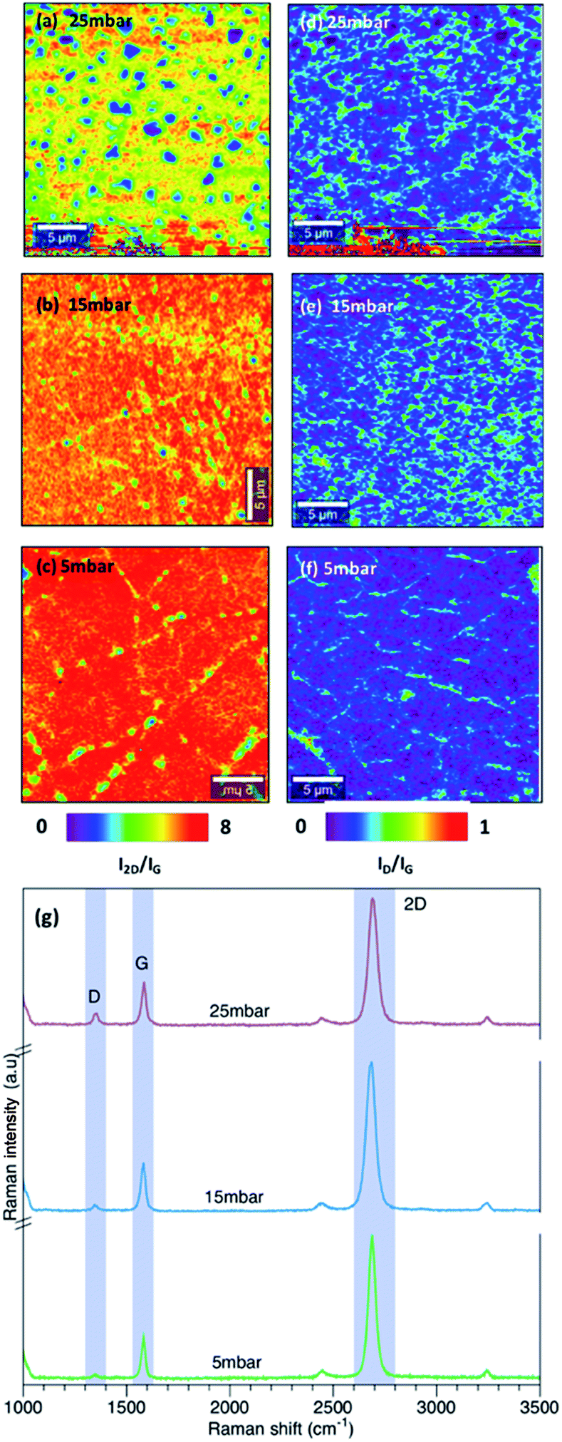 | ||
| Fig. 4 Raman map of I2D/IG intensity at (a) 25 mbar, (b) 15 mbar, (c) 5 mbar and ID/IG intensity at (d) 25 mbar, (e) 15 mbar, (f) 5 mbar (g) Raman spectrum of graphene growth at different pressure. | ||
Under low pressure condition, the growth of graphene is limited by the surface reaction and results in a uniform thickness. Our results are consistent with the analysis done by Bhaviripudi et al.28 in which they investigated the role of the pressure of the reaction chamber in quartz tube reactor at growth temperature of 1000 °C. It has been demonstrated that graphene growth on Cu foil under atmospheric pressure is not self-limited and it is highly affected by the concentration of the gas compositions. Graphene grown under low pressure conditions (0.13–1.3) mbar results in forming monolayer with a uniform thickness. At low pressure, the flux of active species is lower and results in a fewer collision. Lowering the chamber pressure while maintaining the same growth temperatures leads to a growth limited by the surface reaction.
For a monolayer graphene, the intensity of the IG peak intensities become weaker at the grain boundaries.29,30 Fig. 5(a) and (b) shows the IG peak intensity map at 15 mbar and 5 mbar respectively. As shown in Fig. 5(a), graphene synthesized at 15 mbar results in forming a high quality monolayer graphene with grain size greater than 5 μm. Interestingly, graphene synthesized at 5 mbar revealed high quality monolayer graphene with smaller grain size. The reduction in the chamber pressure enhanced the formation of high quality monolayer graphene however it resulted in a decrease in the graphene grain size. Miseikis et al.11 observed a similar behaviour in the graphene crystal size with changing the chamber pressure. In their study, they have shown that decreasing the chamber pressure results in decreasing in the graphene crystal size.
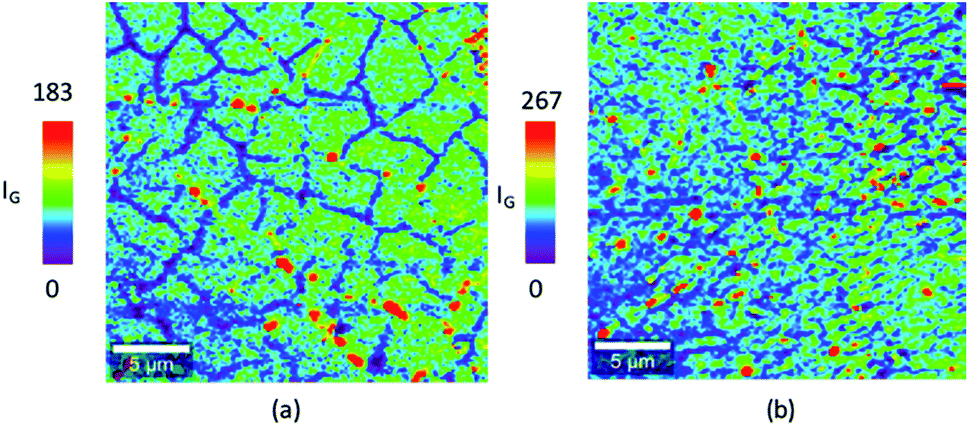 | ||
| Fig. 5 Raman map IG peak intensity at (a) 15 mbar and (b) 5 mbar. | ||
3.3 Effect of hydrogen to methane ratio
At 5 mbar and 1060 °C, the effect of CH4:H2 ratio on graphene growth is investigated. Initially, the growth was done under flow of methane while hydrogen flow rate was set to zero. The methane flow rate was set to 1 and 3 sccm and the growth was done for 1 second to observe the initial domain size of graphene. As shown in Fig. 6(a) and (b), the graphene domains are barely observed indicating very slow rate of graphene growth when the growth is done without any flow of hydrogen. It was also observed that the Cu surface oxidized very quickly highlighting the importance of hydrogen in counteracting the detrimental effects of stray oxygen and or other oxidizing contaminants.31 However, when the hydrogen flow rate is increased to 30 sccm as shown in Fig. 6(c) and (d), graphene domains size increases and becomes larger with higher methane concentration. The results highlight the fact that hydrogen plays a major role in activating the surface for graphene growth. As explained by Vlassiouk et al.,31 the presence of hydrogen facilitates the chemisorption of methane on cupper surface. Reaction (2) describes the methane chemisorption with the presence of hydrogen catalysts.| (CH4)s + H2 ⇔ (CH3)s + H2 | (2) |
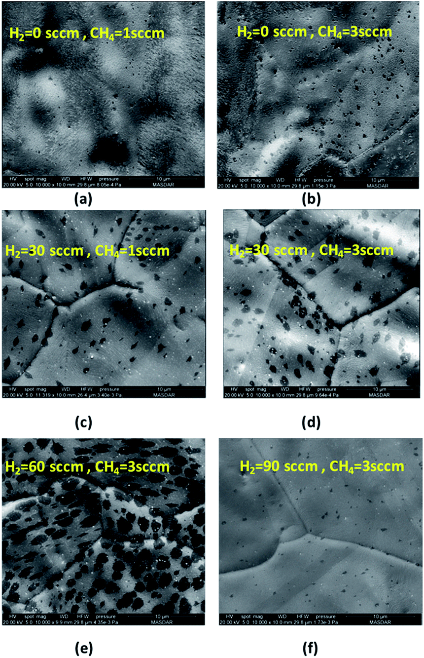 | ||
| Fig. 6 SEM images of graphene domain at different hydrogen to methane ratio. (a) H2 = 0 sccm, CH4 = 1 sccm, (b) H2 = 0 sccm, CH4 = 3 sccm (c) H2 = 30 sccm, CH4 = 1 sccm, (d) H2 = 30 sccm, CH4 = 3 sccm, (e) H2 = 60 sccm, CH4 = 3 sccm, (f) H2 = 90 sccm, CH4 = 3 sccm. | ||
The methane has to be chemisorbed to produce active species such as (CH3)s, (CH2)s, (CH)s or (C)s. The dehydrogenation reactions on Cu surface without hydrogen catalysts is considered unfavourable since it requires high activation barrier (i.e. 1.6 eV) to form (CH3)s radical.30 The existence of hydrogen atoms promotes the activation of physisorbed methane and results in the formation of surface bound (CH3)s radicals. Further dehydrogenation results in producing the other active surface bound which subsequently react to produce graphene.
The effect of hydrogen was further analyzed by fixing the methane flow rate to 3 sccm and changing the hydrogen flow rate to 60 and 90 sccm. As observed in Fig. 6(e) and (f), at 60 sccm of H2, the domain size becomes larger compared to growth done at 30 sccm of H2. As explained previously, higher hydrogen concentration facilitated the activation of Cu surface for graphene growth. However, further increase in H2 flow rate resulted in etching the graphene domain as described in reaction (3).
| (H)s + graphene ⇔ (graphene–C) + (CHx)s | (3) |
This highlights the double role of hydrogen being a catalyst for activating surface-bound carbon and as an etchant that controls the size and morphology of graphene domain.
At 60 sccm of H2, the flow of methane is increased from 3 sccm to 15 sccm to observe the change in graphene domain size and morphology. It has been shown in Fig. 7 that higher methane concentration produced graphene domain with smoother edges compared to irregular edges observed at lower methane concentration. This could be attributed to the fact that higher methane concentration would result in more hydrogen generation during the dehydrogenation process as descried in reaction (2). The increase in hydrogen resulted in etching the edges of graphene domain. The etching resulted in producing less irregular edges and smaller domain size. The above results show that the domain size is highly affected by the concentration of methane and hydrogen. A compromise between hydrogen and methane mixture is required to achieve uniform growth of graphene.
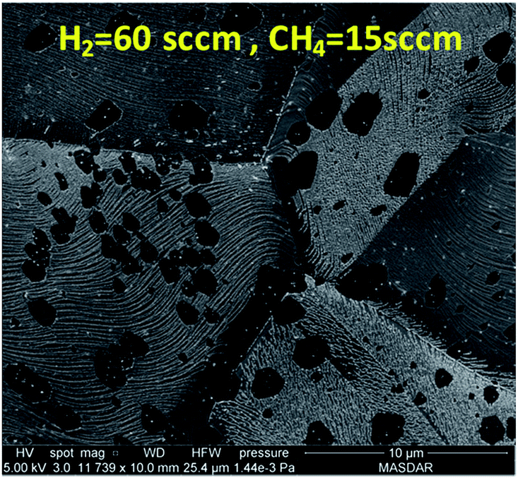 | ||
| Fig. 7 SEM images of graphene domain at grown under H2 = 60 sccm, CH4 = 15 sccm. | ||
After optimizing all the growth parameters for fast production of large area high quality graphene, we characterized the optical and electrical properties of the synthesised graphene. Measured transmission and reflection of monolayer graphene on glass substrate are shown in Fig. 8(a). The monolayer graphene has a negligible reflection <0.1% and an optical opacity of ∼πα = 3.5%. The estimated optical transmittance calculated based on eqn (4)32 is T = 96.6%.
 | (4) |
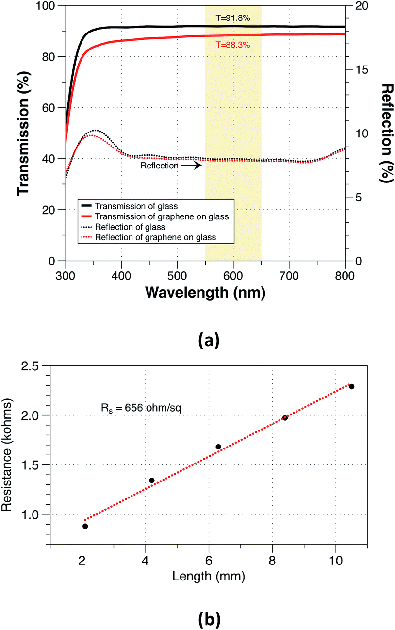 | ||
| Fig. 8 (a)Transmission and reflection of graphene. (b) Sheet resistance of graphene. | ||
The measured optical transmittance is lower than the typical transmittance of 97.7% for monolayer graphene suspended on air. This could be mainly attributed to the use of glass substrate as a reference and the existence of the polymer residue. The sheet resistance was measured as shown in Fig. 8(b) and it was estimated to be approximately 656 ohm/sq which is lower than the reported values of ∼1–2 kohm sq−1 for monolayer CVD graphene.33,34
4. Conclusions
In summary, a detailed study on the synthesis of graphene using cold wall CVD reactor is presented. We have shown that both temperature and pressure play a fundamental role in determining the thickness uniformity of the grown graphene. High temperature with low pressure results in forming a high quality monolayer graphene. We further analyzed the effect of hydrogen to methane ratio and we have shown that the domain size is highly affected by the concentration of methane and hydrogen. Finally, this study provides insight into understanding the effect of growth parameters toward achieving high quality monolayer graphene in 4′′ cold wall CVD reactors that is beneficial for industrial applications.Conflicts of interest
There are no conflicts to declare.Acknowledgements
Authors would like to thank the anonymous reviewers for their valuable comments and suggestions to improve the quality of the paper. A. Alnuaimi would like to thank Leslie George, Adrian clark and Mike Tiner for their technical assistance. This work is fully supported by Masdar Institute.References
- K. S. Novoselov, A. K. Geim, S. V. Morozov, D. Jiang, Y. Zhang and S. V. Dubonos, et al., Electric field effect in atomically thin carbon films, Science, 2004, 306, 666 CrossRef CAS PubMed.
- W. Norimatsu and M. Kusunoki, Epitaxial graphene on SiC {0001}: advances and perspectives, Phys. Chem. Chem. Phys., 2014, 16, 3501 RSC.
- A. Michon, S. Vézian, E. Roudon, D. Lefebvre, M. Zielinski and T. Chassagne, et al., Effects of pressure, temperature, and hydrogen during graphene growth on SiC (0001) using propane-hydrogen chemical vapor deposition, J. Appl. Phys., 2013, 113, 203501 CrossRef.
- S. Chaitoglou, E. Pascual, E. Bertran and J. Andujar, Effect of a balanced concentration of hydrogen on graphene CVD growth, J. Nanomater., 2016, 2016, 54 Search PubMed.
- C. K. Chua and M. Pumera, Chemical reduction of graphene oxide: a synthetic chemistry viewpoint, Chem. Soc. Rev., 2014, 43, 291 RSC.
- S. Abdolhosseinzadeh, H. Asgharzadeh and H. S. Kim, Fast and fully-scalable synthesis of reduced graphene oxide, Sci. Rep., 2015, 5, 10160 CrossRef CAS PubMed.
- Y. Zhang, L. Zhang and C. Zhou, Review of chemical vapor deposition of graphene and related applications, Acc. Chem. Res., 2013, 46, 2329 CrossRef CAS PubMed.
- R. Muñoz and C. Gómez-Aleixandre, Review of CVD synthesis of graphene, Chem. Vap. Deposition, 2013, 19, 297 CrossRef.
- X. Chen, L. Zhang and S. Chen, Large area CVD growth of graphene, Synth. Met., 2015, 210, 95 CrossRef CAS.
- X. Li, W. Cai, J. An, S. Kim, J. Nah and D. Yang, et al., Large-area synthesis of high-quality and uniform graphene films on copper foils, Science, 2009, 324, 13122009 Search PubMed.
- V. Miseikis, D. Convertino, N. Mishra, M. Gemmi, T. Mashoff and S. Heun, et al., Rapid CVD growth of millimetre-sized single crystal graphene using a cold-wall reactor, 2D Mater., 2015, 2, 014006 CrossRef.
- T. H. Bointon, M. D. Barnes, S. Russo and M. F. Craciun, High quality monolayer graphene synthesized by resistive heating cold wall chemical vapor deposition, Adv. Mater., 2015, 27, 4200 CrossRef CAS PubMed.
- W. Mu, Y. Fu, S. Sun, M. Edwards, L. Ye and K. Jeppson, et al., Controllable and fast synthesis of bilayer graphene by chemical vapor deposition on copper foil using a cold wall reactor, Chem. Eng. J., 2016, 304, 106 CrossRef CAS.
- S. Das and J. Drucker, Nucleation and growth of single layer graphene on electrodeposited Cu by cold wall chemical vapor deposition, Nanotechnology, 2017, 28, 105601 CrossRef PubMed.
- L. Tao, J. Lee, H. Li, R. D. Piner, R. S. Ruoff and D. Akinwande, Inductively heated synthesized graphene with record transistor mobility on oxidized silicon substrates at room temperature, Appl. Phys. Lett., 2013, 103, 183115 CrossRef.
- W. Cai, R. D. Piner, Y. Zhu, X. Li, Z. Tan and H. C. Floresca, et al., Synthesis of isotopically-labeled graphite films by cold-wall chemical vapor deposition and electronic properties of graphene obtained from such films, Nano Res., 2009, 2, 851 CrossRef CAS.
- X. Kun, X. Chen, D. Jun, Z. Yanxu, G. Weiling and M. Mingming, et al., Graphene transparent electrodes grown by rapid chemical vapor deposition with ultrathin indium tin oxide contact layers for GaN light emitting diodes, Appl. Phys. Lett., 2013, 102, 162102 CrossRef.
- J. M. Lee, H. Y. Jeong and W. I. Park, Large-scale synthesis of graphene films by Joule-heating-induced chemical vapor deposition, J. Electron. Mater., 2010, 39, 2190 CrossRef CAS.
- L. Huang, Q. Chang, G. Guo, Y. Liu, Y. Xie and T. Wang, et al., Synthesis of high-quality graphene films on nickel foils by rapid thermal chemical vapor deposition, Carbon, 2012, 50, 551 CrossRef CAS.
- J. Ryu, Y. Kim, D. Won, N. Kim, J. S. Park and E.-K. Lee, et al., Fast synthesis of high-performance graphene films by hydrogen-free rapid thermal chemical vapor deposition, ACS Nano, 2014, 8, 950 CrossRef CAS PubMed.
- L. Tao, J. Lee, H. Chou, M. Holt, R. S. Ruoff and D. Akinwande, Synthesis of high quality monolayer graphene at reduced temperature on hydrogen-enriched evaporated copper (111) films, ACS Nano, 2012, 6, 2319 CrossRef CAS PubMed.
- W. Liu, H. Li, C. Xu, Y. Khatami and K. Banerjee, Synthesis of high-quality monolayer and bilayer graphene on copper using chemical vapor deposition, Carbon, 2011, 49, 4122 CrossRef CAS.
- L. Malard, M. Pimenta, G. Dresselhaus and M. Dresselhaus, Raman spectroscopy in graphene, Phys. Rep., 2009, 473, 51 CrossRef CAS.
- L. G. Cançado, A. Jorio, E. H. Martins Ferreira, F. Stavale, C. A. Achete, R. B. Capaz, M. V. O. Moutinho, A. Lombardo, T. S. Kulmala and A. C. Ferrari, Quantifying defects in graphene via Raman spectroscopy at different excitation energies, Nano Lett., 2011, 11, 3190 CrossRef PubMed.
- S. Xing, W. Wu, Y. Wang, J. Bao and S.-S. Pei, Kinetic study of graphene growth: temperature perspective on growth rate and film thickness by chemical vapor deposition, Chem. Phys. Lett., 2013, 580, 62 CrossRef CAS.
- H. Kim, C. Mattevi, M. R. Calvo, J. C. Oberg, L. Artiglia and S. Agnoli, et al., Activation energy paths for graphene nucleation and growth on Cu, ACS Nano, 2012, 6, 3614 CrossRef CAS PubMed.
- C.-S. Chen and C.-K. Hsieh, Effects of acetylene flow rate and processing temperature on graphene films grown by thermal chemical vapor deposition, Thin Solid Films, 2015, 584, 265 CrossRef CAS.
- S. Bhaviripudi, X. Jia, M. S. Dresselhaus and J. Kong, Role of kinetic factors in chemical vapor deposition synthesis of uniform large area graphene using copper catalyst, Nano Lett., 2010, 10, 4128 CrossRef CAS PubMed.
- S. Wang, S. Suzuki and H. Hibino, Raman spectroscopic investigation of polycrystalline structures of CVD-grown graphene by isotope labeling, Nanoscale, 2014, 6, 13838 RSC.
- Q. Yu, L. A. Jauregui, W. Wu, R. Colby, J. Tian and Z. Su, et al., Control and characterization of individual grains and grain boundaries in graphene grown by chemical vapour deposition, Nat. Mater., 2011, 10, 443 CrossRef CAS PubMed.
- I. Vlassiouk, M. Regmi, P. Fulvio, S. Dai, P. Datskos and G. Eres, et al., Role of hydrogen in chemical vapor deposition growth of large single-crystal graphene, ACS Nano, 2011, 5, 6069 CrossRef CAS PubMed.
- R. R. Nair, P. Blake, A. N. Grigorenko, K. S. Novoselov, T. J. Booth, T. Stauber, N. M. Peres and A. K. Geim, Fine structure constant defines visual transparency of graphene, Science, 2008, 320, 1308 CrossRef CAS PubMed.
- C. Mattevi, H. Kim and M. Chhowalla, A review of chemical vapour deposition of graphene on copper, J. Mater. Chem., 2011, 21, 3324 RSC.
- J. W. Suk, A. Kitt, C. W. Magnuson, Y. Hao, S. Ahmed, J. An, A. Swan, B. B. Goldberg and R. S. Ruoff, Transfer of CVD-grown monolayer graphene onto arbitrary substrates, ACS Nano, 2011, 5, 6916–6924 CrossRef CAS PubMed.
| This journal is © The Royal Society of Chemistry 2017 |