
 Open Access Article
 This Open Access Article is licensed under a
 Creative Commons Attribution 3.0 Unported Licence
Vertical Bi2Se3 flake array as a Pt-free counter electrode for dye-sensitized solar cells†
Manshu Han,
Shuang Lu,
Jiangang Ma *,
Haiyang Xu*,
Yinglin Wang,
Xintong Zhang and
Yichun Liu
*,
Haiyang Xu*,
Yinglin Wang,
Xintong Zhang and
Yichun Liu
Centre for Advanced Optoelectronic Functional Materials Research, Key Laboratory for UV Light-Emitting Materials and Technology of Ministry of Education, Northeast Normal University, Changchun 130024, China. E-mail: majg@nenu.edu.cn; hyxu@nenu.edu.cn; Fax: +86 85099772; Tel: +86 431 85099767
First published on 8th November 2017
Abstract
In dye-sensitized solar cells (DSSCs), the catalytic activity and electrical conductivity of the counter electrodes (CEs) is of great importance for the increase of power conversion efficiency (PCE). Although Pt is the most widely used material for CEs of DSSCs, the high price and low abundance of Pt severely limit its application on a large scale and alternative materials are highly desired. In this paper, Bi2Se3 films of vertically aligned flake arrays fabricated by the vapor deposition technique are exploited as Pt-free CEs in DSSCs. Thanks to the excellent surface conductivity and the large number of catalytic active sites of Bi2Se3 flakes, the DSSC with a Bi2Se3 vertical flake array CE exhibited higher PCE than that with regular Pt CEs. This work provides an opportunity to develop practical Pt-free CEs which could facilitate the large-scale application of DSSCs.
Introduction
In the past two decades, dye-sensitized solar cells (DSSCs) have attracted considerable attention from the scientific community and the photovoltaic industry, owing to their low cost, simple production processes, environmental friendliness and high energy conversion efficiency.1–3 As one of the elemental components in DSSCs, counter electrodes (CEs) are of great importance for the reduction rate of triiodide (I3−) to iodide (I−).4 Due to its chemical inertness, good conductivity and catalytic activity, Pt is conventionally used as the CE for catalyzing the reduction of I3−.5 Nevertheless, Pt is a low-abundant element and consequently is extremely expensive, which prevents its large-scale application in DSSCs.6,7 Therefore, great efforts have been devoted to finding proper substitutes for Pt in the past decade. So far, various materials like carbon nanotubes, conductive organic polymers and inorganic semiconductors have been proposed as Pt-free CEs.4,8–12 However, none of them can completely replace Pt because of either low catalytic activity or poor chemical or thermal stability.Recently, an exotic phase of matter, 3D topological insulators like Bi2Se3 and Bi2Te3, have been recognized as a promising material for various electrochemical applications, due to their novel laminar structure and topologically protected metallic surface states. For instance, Chen and his coworkers predicted in their theoretical studies that Au covered topological insulators Bi2Se3 could show improved catalytic activity of CO oxidation because the surface states of Bi2Se3 would increase the adsorption energy of CO and O2 molecules.13 The electrochemical catalytic activity of the topological insulator Bi2Se3 were first demonstrated experimentally by applying the Bi2Se3 modified glass carbon electrode for the detection of glucose in human blood serum, in which the topological insulator facilitates the electron transfer at the interface.14 Ali et al. have successfully synthesized the Bi2Se3 nanosheets by different synthesis methods and compared the electrochemical performance of various Bi2Se3 nanosheets as electrodes of lithium ion batteries for the first time.15 Bi2Se3 can also be used as a potential electrochemical hydrogen storage material like other layered materials, such as MoS2 and so on.16,17 For example, excellent electrochemical hydrogen storage capacity and long cycle life under charge/discharge cycling of Bi2Se3 have been reported recently.18 Although both theoretical and experimental studies indicate that Bi2Se3 has excellent electrochemical activity, to the best of our knowledge no research on the potential of using Bi2Se3 as CEs in DSSCs has been reported so far.
Herein, Bi2Se3 flake films were synthesized by vapor deposition on FTO substrate and were used directly as CEs in DSSCs. Electrochemical measurements show that the morphologies of the Bi2Se3 films will influence the catalytic activity of the CEs significantly. It is found that Bi2Se3 films composed of vertically aligned flake array exhibit outstanding electrocatalytic activity and could be a good candidate to replace Pt as CEs in DSSCs because of the unique surface conductivity and the abundant catalytic active sites of 3D topological insulators.
Experiments
Synthesis and preparation of CEs
The Bi2Se3 flakes were grown on FTO (OPV-FT022-7, America, transmittance 80–82%, square resistance 7–8 Ω, haze 5%, thickness 2.2 mm) by vapor deposition inside a horizontal vacuum tube furnace equipped with a 30 mm diameter quartz tube. The Bi2Se3 powder (5 N) was used as the source of the deposition. FTO substrates were placed at different temperature zones of the downstream away from the source. The tube is pumped down to a base pressure of 8 × 10⁻¹ Pa and then flushed with Ar gas for several times. The Bi2Se3 powder was place at the center of the furnace and was heated up to 550 °C. Subsequently, the Ar was kept flowing at a rate of 65 sccm for 3 h. After the vapor deposition, the furnace was cooled down naturally. For comparison, Pt CEs were prepared by drop-casting 10 mol L−1 of chloroplatinic acid isopropyl alcohol solution on the surface of FTO substrates and subsequently annealing at 450 °C for 30 min.Fabrication of DSSCs
A 10 μm thick layer of 20 nm sized TiO2 particles (TiO2 Paste DSL 18NR-T, Australia) was loaded on the FTO conducting glass by screen printer technique. After sintering at 125 °C, the obtained layer was further coated with a 6 μm thick scattering layer of 200 nm sized TiO2 particles (OPV-TPP200, Yingkou) and sintered at 500 °C for 30 min. After that, the TiO2 films on FTO glass were immersed in a solution of N719 (0.3 mM in aqueous ethanol) dye for 24 h to be used as the dye-sensitized photoanodes. The photoanodes and different CEs were assembled into a sandwich-type cell and separated by a 60 μm thick film (OPV-Surlyn-60, Yingkou) and sealed up. The cell interspace between the photoanode and CE was filled with the I−/I3− redox electrolyte which is composed of 0.05 M LiI, 0.03 M iodine, 0.6 M 1,3-dimethylimidazolium iodide (DMII) ionic liquids, 0.1 M guanidinium thiocyanate (GuSCN), and 0.5 M 4-tert-butylpyridine in anhydrous acetonitrile: valeronitrile (85![[thin space (1/6-em)]](https://www.rsc.org/images/entities/char_2009.gif) :15).19,20 The assembled DSSCs were used to test the photocurrent–voltage (J–V) with an active area of 0.1256 cm2. Identical DSSCs with an active area of 0.64 cm2 were also assembled for electrochemical impedance spectroscopy (EIS) and Tafel-polarization (Tafel) measurements.
:15).19,20 The assembled DSSCs were used to test the photocurrent–voltage (J–V) with an active area of 0.1256 cm2. Identical DSSCs with an active area of 0.64 cm2 were also assembled for electrochemical impedance spectroscopy (EIS) and Tafel-polarization (Tafel) measurements.
Characterization and measurements
The surface morphologies and the crystal structures of the Bi2Se3 CEs were characterized using a FEI Quanta 250 field-emission scanning electron microscope (SEM) and a Rigaku D/MAX 2500 PC X-ray diffractometer with Cu-Kα line radiation. XRD measurements were conducted in a conventional θ/2θ scan mode. The current–voltage characteristics of the DSSCs were measured with a Keithley 2400 source meter under AM 1.5G simulated solar irradiation from a Sun 2000 solar simulator (ABET technology, 100 mW cm−2). The EIS experiments and Tafel-polarization curves were measured in the dark using a Princeton PARSTAT 2273 advanced electrochemical system. EIS was recorded in the frequency range from 100 mHz to 100 kHz with an AC amplitude of 10 mV. The impedance measurements were carried out under a bias of 0 V in the dark. Tafel-polarization measurements were carried out under the bias between −1 to 1 V, with a scan rate of 50 mV s−1.Results and discussion
As reported previously, the surface morphology of Bi2Se3 nanostructures can be tuned by adjusting the substrate temperature and carrier gas flow rate through the vapor transport deposition.21 Therefore, two substrates were placed at different temperature zones in order to obtain two typical Bi2Se3 nanostructures with different morphologies. Fig. 1(a and b) show the surface morphologies of the samples which were grown at 440 °C and 520 °C temperature zones, respectively. A pristine FTO substrate were shown in Fig. 1(d) for comparison purpose. It can be seen that when the substrate was placed at 440 °C temperature zone, a large number of submicron-sized Bi2Se3 flakes were obtained on the FTO substrate, while when the substrate was placed at 520 °C temperature zone, an array of upstanding micron-sized Bi2Se3 flakes were obtained. The surface morphology of the submicron-sized Bi2Se3 flake is in conformity with the FTO substrate, indicating that in the nucleation stage of their self-assembly Bi2Se3 flakes would rather grow along the facets of the FTO micro-crystals on the substrate. Since most of the area in Fig. 1(a) was covered by the terrace of the Bi2Se3 flakes, the sample in Fig. 1(a) is named as the terrace-terminated film. In contrast, the upstanding micron-sized Bi2Se3 flake array is composed of laminar Bi2Se3 flakes with numerous edges. So, the sample in Fig. 1(b) is named as the edge-terminated film. Fig. 1(c) shows the surface morphology of Pt coated FTO substrate, in which Pt nano-crystals can be observed in the valleys of FTO nano-crystals.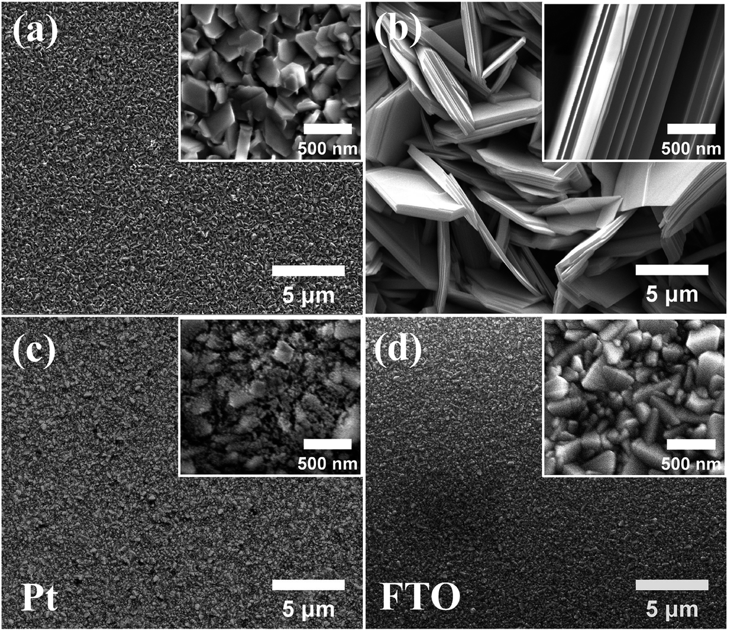 | ||
| Fig. 1 The top-view SEM images of the Bi2Se3 films prepared by vapor deposition at 440 °C and 520 °C temperature zone, respectively (a and b). The top-view SEM image of Pt nano-crystals on the FTO substrate (c). The SEM image of a pristine FTO (d). The insets (a–d) are the corresponding magnified images. | ||
Fig. 2(a and b) show the XRD patterns of the terrace-terminated and the edge-terminated films, respectively. Except the peak from FTO substrate, all the peaks in the XRD patterns can be indexed as rhombohedral Bi2Se3 (JCPDS: 033-0214) which has a layered crystal structure composed of quintuple units stacking along the 〈001〉 direction. Since the XRD spectra were taken in the conventional θ/2θ Bragg–Brentano geometry, only the crystal planes that are parallel to the substrate surface will produce diffraction peaks in the spectra, which would indicate the preferred orientation of nanostructures in the Bi2Se3 films with respect to the substrate surface. In Fig. 2(a) the strong diffraction peaks from (003) and (006) planes indicate that 〈001〉 direction is one of the preferred orientations for the terrace-terminated film. This is consistent with the crystal symmetry of Bi2Se3 and the surface morphology of the terrace-terminated film shown in Fig. 1(a), in which lots of flat Bi2Se3 terraces cover the surface of FTO substrate. In contrast, the edge-terminated film shows very weak (001) diffraction peak and strong (110) peak, indicating that the upstanding flakes in Fig. 1(b) tend to align along 〈110〉 direction which is perpendicular to the substrate surface. However, because the polycrystalline FTO substrates have a relative rough surface, the orientations of both the flat terraces and the upstanding flakes in Fig. 1(a and b) will somehow deviate from the normal of the substrate, which is the main reason for the presence of other diffraction peaks such as (015) and (101) in the XRD spectra.
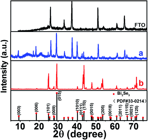 | ||
| Fig. 2 (a and b) are θ/2θ scan XRD patterns of the terrace-terminated film and the edge-terminated Bi2Se3 film grown at 440 °C and 520 °C, respectively. The diffractogram of FTO substrate and the standard PDF card of rhombohedral Bi2Se3 (PDF#00-033-0214) are shown as references. | ||
Fig. 3 shows the photocurrent density–voltage characteristics of N719-sensitized solar cells assembled with the conventional Pt (black square), the edge-terminated Bi2Se3 film (red circle) and the terrace-terminated Bi2Se3 film (blue triangle) as CEs, respectively. The relevant photovoltaic performance parameters including the short-circuit photocurrent density (Jsc), the open-circuit photovoltage (Voc), the fill factor (FF) and the PCE derived from Fig. 3 are listed in Table 1. The DSSC with the edge-terminated Bi2Se3 film as CE the DSSC yielded a PCE of 5.52% (Jsc = 15.67 mA cm−2, Voc = 0.65 V, FF = 0.54), while the DSSC with the terrace-terminated Bi2Se3 film CE produced a PCE of 4.47% (Jsc = 11.57 mA cm−2, Voc = 0.59 V, FF = 0.65). For reference, a PCE of 5.25% (Jsc = 13.60 mA cm−2, Voc = 0.58 V, FF = 0.67) was obtained under the same condition for the DSSC with the conventional Pt CE. The standard deviation values of Jsc, Voc, FF and PCE for the edge-terminated film were calculated to be 0.021, 0.585, 0.017 and 0.36, respectively. For the terrace-terminated Bi2Se3 CEs, the values are 0.005, 0.158,0.009 and 0.11 (Fig. S1 and Table S1†), respectively. The results show that both the edge-terminated film and the terrace-terminated film have good consistency of PCE performance. Jsc increased in the order of terrace-terminated film < Pt < edge-terminated film, and PCE increased in the same order. Obviously, the edge-terminated film performs even better than Pt as the CEs in DSSCs, indicating that upstanding Bi2Se3 flakes film possesses an excellent catalytic activity for the reduction of I3− ions to I−.
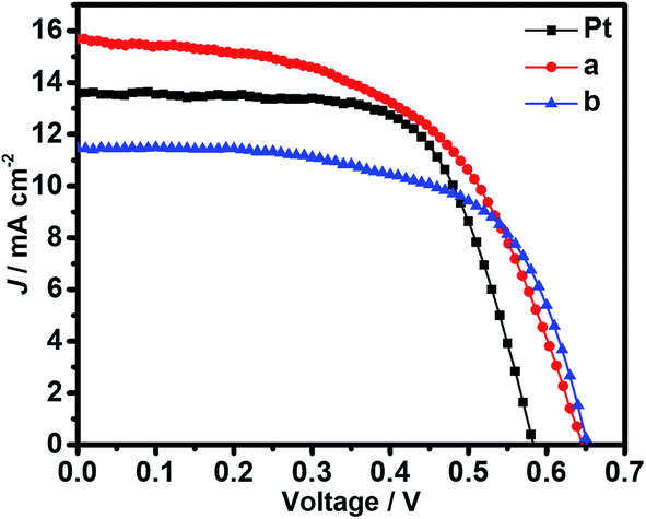 | ||
| Fig. 3 Photocurrent density–voltage characteristics of DSSCs with the conventional Pt, the edge-terminated films (curve a), and the terrace-terminated film (curve b) as CEs, measured at AM 1.5G illumination (100 mW cm−2). | ||
| CE | Voc/V | Jsc/mA cm−2 | FF | PCE/% | Rs/Ω cm2 | Rct/Ω cm2 | Cμ/μF | CPE-P |
|---|---|---|---|---|---|---|---|---|
| Pt | 0.58 | 13.60 | 0.67 | 5.25 | 8.40 | 1.11 | 17.9 | 0.94 |
| Sample-a | 0.65 | 15.67 | 0.54 | 5.52 | 7.20 | 0.92 | 20.9 | 0.99 |
| Sample-b | 0.65 | 11.46 | 0.63 | 4.71 | 6.75 | 6.64 | 9.2 | 0.95 |
To further evaluate the electrochemical characteristics of the Bi2Se3 CEs for the reduction of I3− ion, the EIS experiments were carried out using the symmetrical dummy cells with an active area of 0.64 cm2. Fig. 4 shows the Nyquist plots for the symmetrical dummy cells with the conventional Pt, the edge-terminated and the terrace-terminated Bi2Se3 CEs. Two semicircles in the Nyquist plots can be observed in the high-frequency (left semicircle) and low-frequency (right semicircle) regions, respectively. Generally, the high-frequency intercept on the real axis (Z′ axis) gives the series resistance (Rs) and the diameter of the semicircle in the high-frequency regions is assigned to the charge-transfer resistance (Rct).22 It is known that in EIS measurements the Rs value basically represent the ohmic resistance of the entire circuit including the resistance of CEs and FTO as well as other contact resistance, while the Rct value is negatively proportional to the catalytic activity of the electrode on reduction of I3− ion.23 Cμ is a constant phase element in the equivalent circuit diagram and typify the double-layer capacitance at the interface of CE/electrolyte due to the accumulation of ions on the electrode surface, which is proportional to the active catalytic surface areas of CEs,5,12 CPE-P is the degree of the dispersion. The EIS data including Rs, Rct and Cμ were derived by fitting the Nyquist plots with Z-view software with the equivalent circuit diagram shown as the insert of Fig. 4.4 The fitted results are also listed in Table 1.
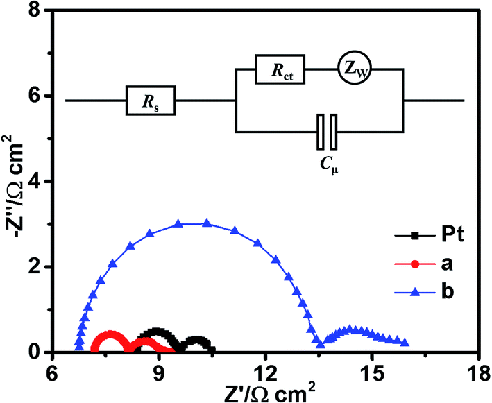 | ||
| Fig. 4 Nyquist plots for the symmetric cells with the edge-terminated (red circles) and the terrace-terminated Bi2Se3 films (blue triangles) as CEs. Pt CE was also presented for reference (black squares). The EIS were measured with a frequency range from 100 kHz to 100 mHz, and the amplitude of the alternating current was set to 10 mV. Insert is the equivalent circuit diagram. | ||
Per the fit parameters of EIS data (see Table 1), the Rs values of cells with the edge-terminated and the terrace-terminated Bi2Se3 electrodes are 7.20 Ω cm2 and 6.75 Ω cm2, respectively, both of which are smaller than that of cell with Pt electrode (8.40 Ω cm2), indicating that Bi2Se3 flake electrodes have better electrical conductivity than Pt electrode. However, it has been reported that the bulk resistivity of Bi2Se3 is two orders of magnitude higher than that of Pt (10.6 × 10⁻⁶ ohm cm).24 According to Hall measurements, Bi2Se3 flake films have Hall mobilities of 510 cm2 V−1 s−1 and 570 cm2 V−1 s−1, respectively, which are both higher than that of bulk material with the same carrier concentration.25–27 Therefore, the small Rs value obtained with the edge-terminated and the terrace-terminated Bi2Se3 electrodes can be partially attributed to the transportation by a topologically protected surface state rather than the transportation in the bulk of Bi2Se3 alone.14 As shown in Table 1, the Rct values with the Pt, the edge-terminated and the terrace-terminated Bi2Se3 electrodes are 1.11, 0.92, and 6.64 Ω cm2, respectively. The edge-terminated Bi2Se3 CE gives the minimum Rct value among all the CEs, indicating that the edge-terminated Bi2Se3 films have the best catalytic activity among the three electrodes.
To further investigate the electrochemical characteristics of Bi2Se3 and Pt electrodes, the Tafel polarization curves were measured on the symmetrical cells used in EIS experiments, as shown in Fig. 5. It shows the current density (J) as a function of voltage (V) at room temperature for the reduction of I3− to I−. The slopes of the tangent to the anodic or cathodic branches are in the order of edge-terminated film > Pt > terrace-terminated film. A large slope in the anodic or cathodic branches indicates a higher exchange current density (J0) on the electrode. Therefore, the edge-terminated film has the best catalytic activity.
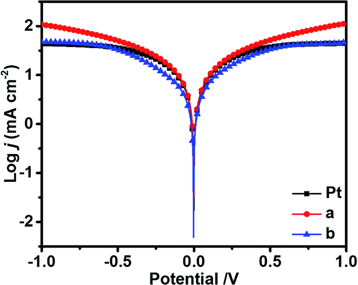 | ||
| Fig. 5 Tafel polarization curves of the I3−/I− symmetrical cells fabricated with the edge-terminated films (red curve), the terrace-terminated films (blue curve) and the Pt (black curve) different CEs. | ||
On the other hand, J0 can also be calculated by the following eqn (1).
 | (1) |
Because the surface morphologies of the edge-terminated, the terrace-terminated Bi2Se3 films and the Pt CEs are so different from each other, it is necessary to evaluated the active catalytic surface areas of each CE by comparing the equivalent capacitance Cμ. The relevant degree of the dispersion (CPE-P) are all above 0.9. Therefore, Cμ can be regarded as a pure capacitor. As show in Table 1, the Cμ of the edge-terminated Bi2Se3 film (20.9 μF) is 10% larger than that of the Pt (17.9 μF) and is one time larger than that of the terrace-terminated Bi2Se3 electrodes (9.2 μF). The edge-terminated Bi2Se3 film CE has the largest active catalytic surface area, which could be tentatively ascribed to the special structure of upstanding micron-sized flake array.
As can be seen in Fig. 1, the edge-terminated Bi2Se3 film is composed of upstanding flakes with lengths of sides up to several microns, while the terrace-terminated film is composed of lying flakes whose sizes are about ten times smaller than that of the edge-terminated Bi2Se3 film. On the other hand, the cross-sectional SEM image (no shown here) indicated that the height of the upstanding flake of the edge-terminated film is in the range of 5–8 microns and both sides of each flake are exposed and consequently could contact with the electrolyte. Then, the ratio of total contact surface area to the substrate area of 41 and 1.4 for the edge-terminated (Fig. 1(b)) and the terrace-terminated samples (Fig. 1(a)), respectively. In spite of the distinct difference of the ratios between the two series of samples, the Cμ of the edge-terminated Bi2Se3 CE is only two times of that of the terrace-terminated Bi2Se3 CE. Therefore, we think that not all the contact surface will contribute equally to the catalytic activity of Bi2Se3 CEs, but the amount of active sites like steps and edges will make a difference.
It is shown in XRD spectra that both the edge-terminated and the terrace-terminated Bi2Se3 films have rhombohedral structure which has a six-fold symmetry along the 〈001〉 direction. So, the hexagonal terraces of the flakes in Fig. 1 should belong to the {001} planes and the six lateral rectangle facets should belong to the {100} planes of Bi2Se3.21 It is known that {001} planes have the lowest surface energy among all the crystal planes of Bi2Se3 and catalytic reactions will most likely take place at planes with high surface energy.28 Although both the surface area of {001} and {100} planes increased with the increasing size and thickness of flakes in the edge-terminated film, the catalytic activity will mainly benefit from the increase of {100} surface area.
Furthermore, it can be noticed in the inset of Fig. 1(b) that there are many steps that can be observed at edges of upstanding Bi2Se3 flakes, which is common for vapor deposition of materials with laminated structures. Since the Bi2Se3 flakes were constructed by stacking Bi2Se3 quintuple layers, the fluctuation of growth rate in different layers results in the presence of steps near the edge of the flakes. With the increasing size and thickness of flakes the number of steps will increase consequently. Considering that the steps could have even higher free energies than the adjacent planes, one can expect that I3− ions could be efficiently reduced to I− at the active sites of those steps. Therefore, the high catalytic activity of the edge-terminated Bi2Se3 film can be attributed to the increase of both the surface area of {100} planes and the length of steps.
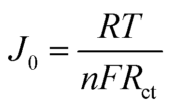
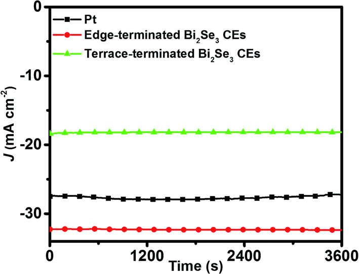
Since stability is one of the most important factors for the practical application of CE,4,29,30 we performed successive current–time and EIS tests to examine the stability of the edge-terminated film and the terrace-terminated film of Bi2Se3 flakes CEs. During the current–time test, the current density of the edge-terminated film and terrace-terminated film of Bi2Se3 flakes CEs maintained 99.7 and 98.7% of the original current after 3600 seconds at −0.25 V, respectively (Fig. 6). The EIS tests on dummy cells were conducted for 8 cycles, after which there was negligible change in Rct for the edge-terminated Bi2Se3 and Pt CEs. However, Rct increased from 6.64 to 23.44 Ω cm2 for the terrace-terminated Bi2Se3 CEs (Fig. 7(b)), due to Bi2Se3 flakes peeling off from the FTO surface during the tests. In addition, Rs is almost unchanged for all the samples, meaning that the continuous cycling hardly influenced the series ohm resistance.
 | ||
| Fig. 6 Current density vs. time plots of Pt and Bi2Se3 CEs under −0.25 V bias voltage. | ||
 | ||
| Fig. 7 Nyquist plots of EIS for the symmetrical cells with the edge-terminated Bi2Se3 sample-a (a), the terrace-terminated Bi2Se3 sample-b (b), and Pt (c) CEs. EIS tests at 0 V from 100 kHz to 100 mHz was performed continuously for 8 times. | ||
Conclusions
In summary, the edge-terminated film and terrace-terminated film of Bi2Se3 flakes have been grown on the surface of FTO through vapor transport deposition and are exploited as CEs in DSSCs. SEM, XRD, PCE and EIS measurements indicate that the edge-terminated film of Bi2Se3 flakes exhibit a better catalytic activity for the reduction of I3− than the Pt CE. It is found that the superior catalytic activity of the edge-terminated Bi2Se3 CE can be understood from two aspects. One is the increase of active sites with the increasing surface area of {100} planes and the length of steps that have higher surface energy. The other is the good charge transportation though the topologically protected surface states of Bi2Se3 flakes. The unique structure of upstanding Bi2Se3 flake array is a good example for utilizing layered topological insulator as effective catalytic materials.Conflicts of interest
There are no conflicts to declare.Acknowledgements
The work was supported by the NSFC (No. 51172041, 51202026, 91233204, 51372035, and 51422201), the NCET Program (Nos. 20120043110002, 20110043120004, and 20130043110004), 973 Program (No. 2012CB933703), “111” project (No. B13013), the Fund from Jilin Province (No. 20140309012GX and 20140201008GX), the Fundamental Research Funds for the Central Universities (No. 2412015BJ003), the Doctoral Fund of Ministry of Education of China (No. 20110043120004), and the Fundamental Research Fund of Ministry of Education of China (No. 113020A), and No. SKLLIM1404.References
- B. O'Regan and M. Grätzel, Nature, 1991, 353, 737–740 CrossRef.
- M. Grätzel, Nature, 2001, 414, 338–344 CrossRef PubMed.
- A. Hagfeldt, G. Boschloo, L. Sun, L. Kloo and H. Pettersson, Chem. Rev., 2010, 110, 6595–6663 CrossRef CAS PubMed.
- F. Gong, H. Wang, X. Xu, G. Zhou and Z.-S. Wang, J. Am. Chem. Soc., 2012, 134(26), 10953–10958 CrossRef CAS PubMed.
- Y. Hou, D. Wang, X. H. Yang, W. Q. Fang, B. Zhang, H. F. Wang, G. Z. Lu, P. Hu, H. J. Zhao and H. G. Yang, Nat. Commun., 2013, 4, 1583 CrossRef PubMed.
- N. Papageorgiou, Coord. Chem. Rev., 2004, 248, 1421–1446 CrossRef CAS.
- G. Calogero, P. Calandra, A. Irrera, A. Sinopoli, I. Citro and G. Dimarco, Energy Environ. Sci., 2011, 4, 1838–1844 CAS.
- A. Kay and M. Grätzel, Sol. Energy Mater. Sol. Cells, 1996, 44, 99–117 CrossRef CAS.
- F. Gong, H. Wang and Z.-S. Wang, Phys. Chem. Chem. Phys., 2011, 13, 17676–17682 RSC.
- Q. H. Li, J. H. Wu, Q. W. Tang, L. Zhang, P. J. Li, J. M. Lin and L. Q. Fan, Electrochem. Commun., 2008, 10, 1299–1302 CrossRef CAS.
- G. R. Li, J. Song, G. L. Pan and X. P. Gao, Energy Environ. Sci., 2011, 4, 1680–1683 CAS.
- M. Wu, X. Lin, A. Hagfeldt and T. Ma, Angew. Chem., Int. Ed., 2011, 50, 3520–3524 CrossRef CAS PubMed.
- H. Chen, W. Zhu, D. Xiao and Z. Zhang, Phys. Rev. Lett., 2011, 107(5), 056804 CrossRef PubMed.
- S. Chen, Y. M. Fang, J. Li, J. J. Sun, G. N. Chen and H. H. Yang, Biosens. Bioelectron., 2013, 46, 171–174 CrossRef CAS PubMed.
- Z. Ali, C. Cao, J. Li, Y. Wang, T. Cao, M. Tanveer, M. Tahir, F. Idrees and F. K. Butt, J. Power Sources, 2013, 229, 216–222 CrossRef CAS.
- J. Chen, N. Kuriyama, H. Yuan, H. T. Takeshita and T. Sakai, J. Am. Chem. Soc., 2001, 123, 11813–11814 CrossRef CAS PubMed.
- B. Zhang, X. C. Ye, W. Dai, W. Y. Hou and X. Yi, Chem.–Eur. J., 2006, 12, 2337–2342 CrossRef CAS PubMed.
- Z. Sun, S. Liufu, X. Chen and L. Chen, Chem. Commun., 2010, 46, 3101–3103 RSC.
- P. Sun, X. Zhang, L. Wang, F. Li, Y. Wei, C. Wang and Y. Liu, New J. Chem., 2015, 39(6), 4845–4851 RSC.
- Z. Jin, Y. Wang, S. Chen, G. Li, L. Wang, H. Zhu, X. Zhang and Y. Liu, RSC Adv., 2016, 6(13), 10450–10455 RSC.
- M. Han, J. Ma, H. Xu and Y. Liu, CrystEngComm, 2015, 17(44), 8449–8456 RSC.
- F. Fabregat-Santiago, J. Bisquert, E. Palomares, L. Otero, D. Kuang, S. M. Zakeeruddin and M. Grätzel, J. Phys. Chem. C, 2007, 111, 6550–6560 CAS.
- J. Chen, K. Li, Y. Luo, X. Guo, D. Li, M. Deng, S. Huang and Q. Meng, Carbon Balance Manage., 2009, 47, 2704–2708 CAS.
- J. Suh, D. Fu, X. Liu, J. K. Furdyna, K. M. Yu, W. Walukiewicz and J. Wu, Phys. Rev. B: Condens. Matter Mater. Phys., 2014, 89, 115307 CrossRef.
- P. Janíček, Č. Drašar, L. Beneš and P. Lošťák, Cryst. Res. Technol., 2009, 5, 505–510 CrossRef.
- K. Jacob John, B. Pradeep and M. Elizabeth, Solid State Commun., 1993, 85(10), 879–881 CrossRef.
- F.-T. Huang, M.-W. Chu, H. H. Kung, W. L. Lee, R. Sankar, S.-C. Liou, K. K. Wu, Y. K. Kuo and F. C. Chou, Phys. Rev. B: Condens. Matter Mater. Phys., 2012, 86, 081104 CrossRef.
- S. Wang, H. Chen, G. Gao, T. Butburee, M. Lyu, S. Thaweesak, J. Yun, A. Du, G. Liu and L. Wang, Nano Energy, 2016, 24, 94–102 CrossRef CAS.
- L. Kavan, J. H. Yum and M. Grätzel, ACS Nano, 2011, 5, 165–172 CrossRef CAS PubMed.
- S. Lu, Y. Wang, F. Li, G. Yang, H. Yang, X. Zhang and Y. Liu, J. Phys. Chem. C, 2017, 121, 12524–12530 CAS.
Footnote |
| † Electronic supplementary information (ESI) available. See DOI: 10.1039/c7ra05117d |
| This journal is © The Royal Society of Chemistry 2017 |