
 Open Access Article
 This Open Access Article is licensed under a
 Creative Commons Attribution 3.0 Unported Licence
Ultra-simple white organic light-emitting diodes employing only two complementary colors with color-rendering index beyond 90
Yanqin Miao *ab,
Kexiang Wangab,
Bo Zhaoab,
Long Gaoab,
Jiacong Xuab,
Hua Wang*ab and
Bingshe Xuab
*ab,
Kexiang Wangab,
Bo Zhaoab,
Long Gaoab,
Jiacong Xuab,
Hua Wang*ab and
Bingshe Xuab
aKey Laboratory of Interface Science and Engineering in Advanced Materials of Ministry of Education, Taiyuan University of Technology, Taiyuan, 030024, PR China. E-mail: miaoyanqin@tyut.edu.cn; wanghua001@tyut.edu.cn; Fax: +86-351-6010311; Tel: +86-351-6014852
bResearch Center of Advanced Materials Science and Technology, Taiyuan University of Technology, Taiyuan, 030024, PR China
First published on 25th October 2017
Abstract
White organic light-emitting diodes (WOLEDs) with an ultra-high color rendering index (CRI) (≥90) are considered to be crucial for special lighting applications, such as in hospitals, art galleries, and museums. However, most reported WOLEDs with a CRI of ≥90 almost all use three or more emitters, and usually suffer from a complicated device structure. In this work, an exciplex formed between a 4,4′,4′′-tris(N-3-methylphenyl-N-phenyl-amino)triphenylamine (m-MTDATA) donor and a bis[2-(2-hydroxyphenyl)-pyridine]beryllium (Bepp2) acceptor, exhibiting a broad-spectrum emission, was employed as a yellow emitter. And a thin 4,4′,4′′-tri(9-carbazoyl)triphenylamine (TCTA) layer (2–6 nm) as a carrier adjustment layer was inserted into the Bepp2 layer of the exciplex to block some of the electrons at the TCTA/Bepp2 interface, inducing a blue light emission from Bepp2. A series of ultra-simple di-chromatic WOLEDs, using only three organic materials, were demonstrated. By changing the thickness of TCTA, the proposed WOLEDs achieve an ultra-high CRI of 92, which, to our knowledge, is by far the simplest structure for a complementary WOLED with a CRI over 90. Besides, the optimized WOLED, at a practical luminance of 3000 cd m−2, shows an ultra-high CRI of 90, and also realizes a high maximum current efficiency and power efficiency of 8.7 cd A−1 and 10.1 lmW−1, respectively. This novel design concept provides a new avenue for achieving simple-structured, but ultra-high-CRI WOLEDs.
Introduction
White organic light-emitting diodes (WOLEDs) have been recognized as a promising alternative display and solid-state lighting technology due to the advantages of low-voltage operation, fast response, wide-viewing angle, easy fabrication of a potentially large area and mechanical flexibility.1–7 For lighting applications, the color rendering index (CRI) is an important indicator because the object under different light sources may look different due to the different colors of the reflected light from the light sources. It is therefore crucial to develop ultra-high-CRI white-light illumination (CRI ≥ 90), especially for lighting applications in hospitals, art galleries, museums, and other special commercial places, etc.8,9To generate white light with an ultra-high CRI, the emission spectrum should be as broad and as continuous as possible in the visible-light spectral region.10 To date, a lot of endeavor has been undertaken to obtain ultra-high-CRI WOLEDs.11–28 For example, Chang et al. demonstrated an efficient three-component phosphorescent WOLED with green/orange–red emitting layers sandwiched between two deep-blue emitting layers, realizing a maximum CRI of up to 94.18 Sun et al., employing four organic dyes to broaden the emission spectrum, developed a hybrid WOLED with an ultra-high CRI up to 94.24 Jou et al. doped five organic dyes into two different phosphorescent and fluorescent emissive layers separated by a high triplet-energy interlayer to fabricate a very-high-CRI (93) WOLED.26 It is found that ultra-high-CRI WOLEDs are generally obtained by employing three-color emitters (red, green, blue), four-color emitters (red, yellow, green, blue) or even more, but the use of more emitters inevitably brings about a complicated device structure, high cost, and low reproducibility, which are detrimental to the commercial development of WOLED lighting products.
Recently, exciplexes have been widely used in WOLEDs for their potential high efficiency and wide spectrum emission, and the wide spectrum is favorable for structuring high-CRI WOLEDs.29–33 In 2014, Hung et al. employed tandem emitting units consisting of blue and yellow exciplexes to demonstrate an exciplex-based WOLED with a CRI over 70.29 Afterwards, Liu et al. utilized incomplete energy transfer from a blue exciplex to a red phosphorescent material to develop a complementary hybrid WOLED, and the white device realized a warm white light with a CRI of 77.30 The CRIs for these exciplex-based WOLEDs are obviously less than the threshold value of 80 for WOLEDs used in lighting, limiting their applications in solid state lighting. Very recently, Han et al. fabricated a two-color WOLED with an ultra-high CRI value of 90.8 by devising a device structure with a red exciplex formed between two blue emitters in a single emitting layer.31 Although an ultra-high CRI is obtained, a relatively complex device structure, requiring accurate control of doping concentration, leads to high fabrication cost and low reproducibility.
In this work, 4,4′,4′′-tris(N-3-methylphenyl-N-phenyl-amino)triphenylamine (m-MTDATA) and bis[2-(2-hydroxyphenyl)-pyridine]beryllium (Bepp2), forming an exciplex exhibiting a broad-spectrum emission, was employed as a yellow emitter. By inserting a thin 4,4′,4′′-tri(9-carbazoyl)triphenylamine (TCTA) layer (2–6 nm) into the Bepp2 layer of the exciplex, a series of ultra-simple di-chromatic WOLEDs, using only three organic materials, were demonstrated, where the thin TCTA layer was used as a carrier adjustment layer (CAL) to block some of the electrons at the TCTA/Bepp2 interface, inducing a blue light emission from Bepp2. By changing the thickness of TCTA, the proposed WOLEDs achieved an ultra-high CRI of 92, which, to our knowledge, is by far the simplest structure of complementary WOLEDs with a CRI over 90. In addition, such an ultra-high CRI is even comparable with other reported three-color, four-color, and five-color WOLEDs. Moreover, the optimized WOLED, at a practical luminance of 3000 cd m−2, shows an ultra-high CRI of 90, and also realizes a high maximum current efficiency (CE) and power efficiency (PE) of 8.7 cd A−1 and 10.1 lm W−1.
Experimental
In this work, organic materials (Bepp2, m-MTDATA, and TCTA), LiF, MoO3, and Al were purchased from commercial sources, and all materials without further purification were directly used to fabricate OLEDs.OLEDs were fabricated on pre-patterned indium tin oxide (ITO) glass substrates with a sheet resistance of 15 Ω per square. Prior to preparation of the OLEDs, the ITO substrates were sequentially cleaned with detergent, acetone, isopropyl alcohol and deionized water for 20 minutes each. And they were treated with UV ozone to improve the work function. Afterwards, they were loaded in a vacuum chamber for deposition of organic layers using thermal evaporation under a base pressure of 5 × 10⁻⁴ Pa. The deposition rates and film thicknesses were controlled by calibrated crystal quartz sensors. Deposition rates for organic materials, LiF, MoO3, and Al were 1 Å s−1, 0.1 Å s−1, 0.3 Å s−1, and 3–6 Å s−1, respectively. The overlap between the ITO anode and the Al cathode is 3 mm × 3 mm, defined as the active emissive area. The organic films for the PL test were deposited on the quartz substrate in the same way as the devices.
The electroluminescence (EL) spectra, CRI, Commission Internationale de L'Eclairage (CIE) coordinates of OLEDs were measured using a computer-controlled PR-655 spectra scan spectrometer. The current density–voltage–luminance (J–V–L) characteristics were measured by a computer-controlled Keithley 2400 source integrated with a BM-70A luminance meter. CE and PE were calculated from the J–V–L curve. The PL spectra of the films were monitored by a Fluoromax-4 luminescence spectrometer. All samples were characterized immediately after thin film deposition without encapsulation.
Results and discussion
In order to demonstrate the exciplex formation between the m-MTDATA donor and Bepp2 acceptor, the normalized photoluminescence (PL) spectra of m-MTDATA, Bepp2 and m-MTDATA:Bepp2 mixed films were investigated and are depicted in Fig. 1. Here, the weight ratio of m-MTDATA to Bepp2 in the mixed film is 1![[thin space (1/6-em)]](https://www.rsc.org/images/entities/char_2009.gif) :1. The m-MTDATA:Bepp2 mixed film shows a featureless PL spectrum located in the yellow-green wave-band with a peak at 540 nm that is obviously red-shifted compared to the intrinsic emission spectra with peaks at 427 nm for m-MTDATA and at 448 nm for Bepp2, indicating that m-MTDATA and Bepp2 molecules can form an exciplex under the conditions of excitation.34,35 In addition, it is found that the m-MTDATA:Bepp2 exciplex exhibits a broad emission spectrum with a full width at half maximum of over 100 nm, nearly covering the visible-light wavelength range from 400 nm to 700 nm, which proves its great potential to construct a high-CRI WOLED.
:1. The m-MTDATA:Bepp2 mixed film shows a featureless PL spectrum located in the yellow-green wave-band with a peak at 540 nm that is obviously red-shifted compared to the intrinsic emission spectra with peaks at 427 nm for m-MTDATA and at 448 nm for Bepp2, indicating that m-MTDATA and Bepp2 molecules can form an exciplex under the conditions of excitation.34,35 In addition, it is found that the m-MTDATA:Bepp2 exciplex exhibits a broad emission spectrum with a full width at half maximum of over 100 nm, nearly covering the visible-light wavelength range from 400 nm to 700 nm, which proves its great potential to construct a high-CRI WOLED.
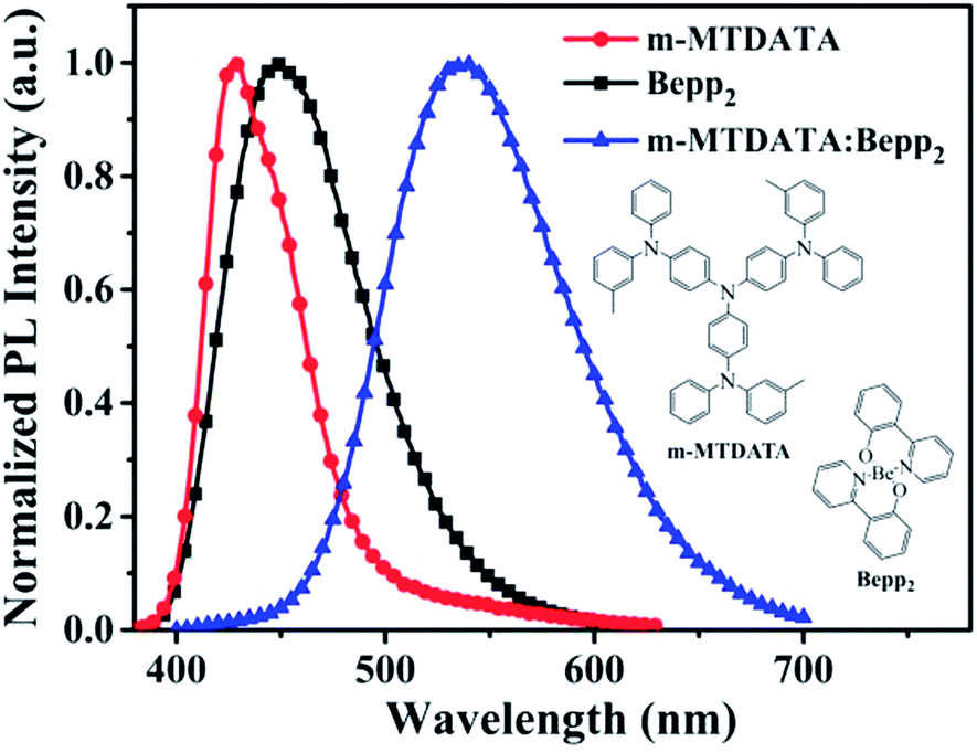 | ||
| Fig. 1 Normalized PL spectra of m-MTDATA, Bepp2 and m-MTDATA:Bepp2 mixed films (weight ratio: 1:1). The inset is the molecular structure of m-MTDATA and Bepp2. | ||
To generate white light emission, OLEDs using fewer emitters (i.e. two complementary colors) while retaining a high CRI is considered to be one of the most effective methods, since it would vastly simplify the device structure of the WOLED.6,11,12,15 It is found that the acceptor (Bepp2) of the above yellow exciplex is not only a widely used electron transporting material, but is also a highly efficient blue fluorescent emitter with a high fluorescent quantum yield of >0.80.22 And the PL emission peak for Bepp2 is located at about 450 nm, which is complementary to the yellow emission of m-MTDATA and Bepp2 forming the exciplex. So, it is natural to come up with a white device realized by combining the emission of the yellow exciplex emitter and the blue emission of Bepp2 simultaneously.
Based on the above analysis, an x nm-thick TCTA layer was inserted into the electron transport layer (ETL) Bepp2 to fabricate a series of yellow and white OLEDs with the following structures: ITO/m-MTDATA (20 nm)/Bepp2 (4 nm)/TCTA (x nm)/Bepp2 (46 nm)/LiF (1 nm)/Al (100 nm). Here, x was set at 0, 2, 3, and 4, corresponding to devices Y1, W1, W2, W3, respectively. Here, an OLED with x = 0 (device Y1), a yellow exciplex device, is selected as a reference, while OLEDs with x = 2–4 nm are the proposed white devices (devices W1, W2, and W3). In these devices, a 20 nm-thick m-MTDATA layer was typically used as hole transport layer (HTL) and the donor of the exciplex, and a 46 nm-thick Bepp2 layer was typically used as an ETL. The x nm-thick TCTA was used as a CAL, which allows some of the electrons to be blocked in the TCTA/Bepp2 interface and then combined with the leaked holes from the TCTA layer, generating blue light from Bepp2 because of a higher LUMO level (−2.4 eV) than Bepp2 (−2.6 eV) and a typical hole transport characteristic for TCTA. Meanwhile, some of the electrons can pass through an x nm-thick TCTA and finally be transported to the m-MTDATA/Bepp2 interface under forward bias, generating broad-spectrum yellow light from the exciplex. This is because a thin organic layer with a thickness of ≤4 nm may not form a neat layer, so a tunnelling effect can occur easily.22,33,36 The 4 nm-thick Bepp2 was used as an exciplex acceptor to form an interfacial exciplex with an m-MTDATA donor, and was also used as a CAL, which allows some of the holes to tunnel through it and finally contribute to the emission of Bepp2 as in the case of TCTA, inducing a white emission. The detailed device structure and working mechanism diagram for devices Y1, W1, W2, and W3 are shown in Fig. 2.
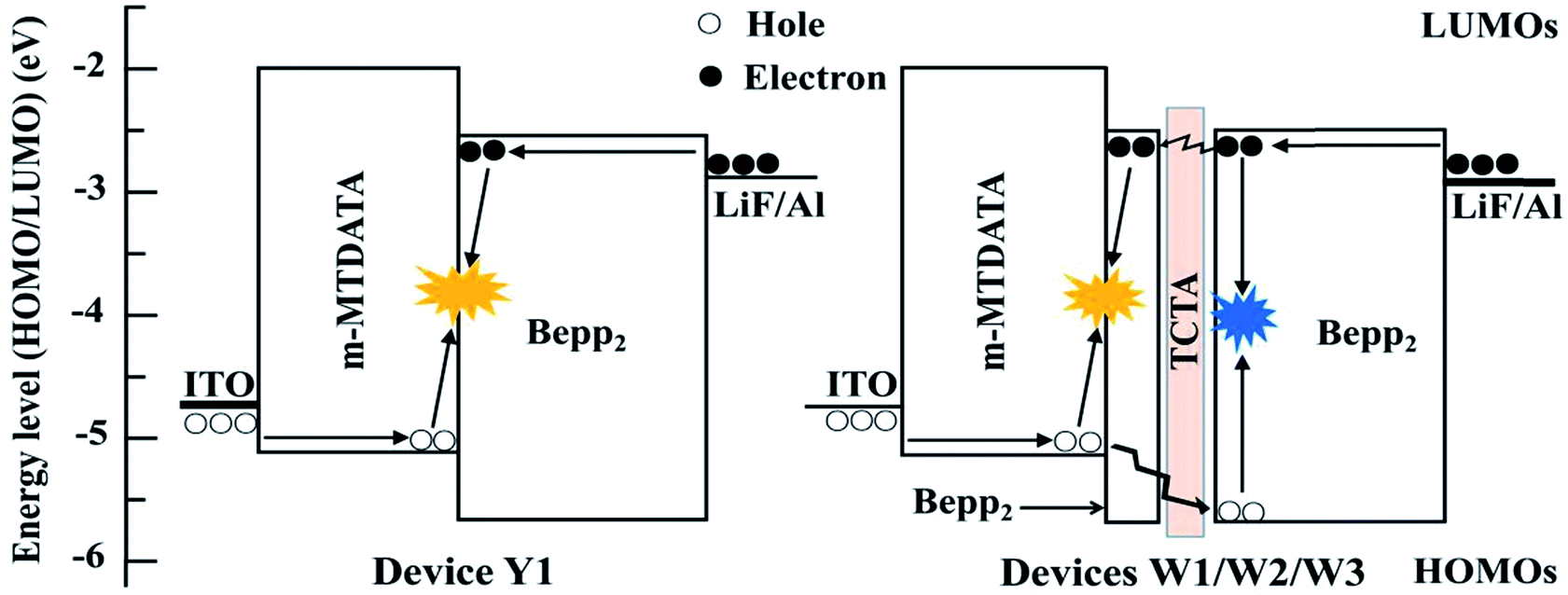 | ||
| Fig. 2 Device structure and working mechanism diagram for the devices Y1, W1, W2, and W3. | ||
Fig. 3 depicts the normalized EL spectra of different devices at different luminances. From Fig. 3(a), a broad yellow emission peak at about 560 nm is observed, which is assigned to the emission of the m-MTDATA/Bepp2 exciplex. Compared with the PL spectrum with an emission peak located at about 540 nm, a big red-shift of about 20 nm in the EL spectra is observed, which should be derived from the inherent characteristics of the exciplex. Such red-shifts of the EL spectra are also observed in other exciplexes.37,38 When the luminance increases from 100 cd m−2 to 3000 cd m−2, the emission spectrum of the yellow exciplex has a slight blue-shift along with the emergence of a shoulder located at about 440 nm, which should be ascribed to the intrinsic emission of m-MTDATA or Bepp2. The reason is that the exciplex is generally formed at the donor/acceptor interface, whereas there is only one heterojunction interface in device Y1, leading to insufficient formation of exciplex. Therefore, under high current density, some of the holes and electrons will inevitably overcome the energy barrier of the m-MTDATA/Bepp2 interface and inject into the adjacent ETL and HTL, respectively, causing the emissions of m-MTDATA and Bepp2.39
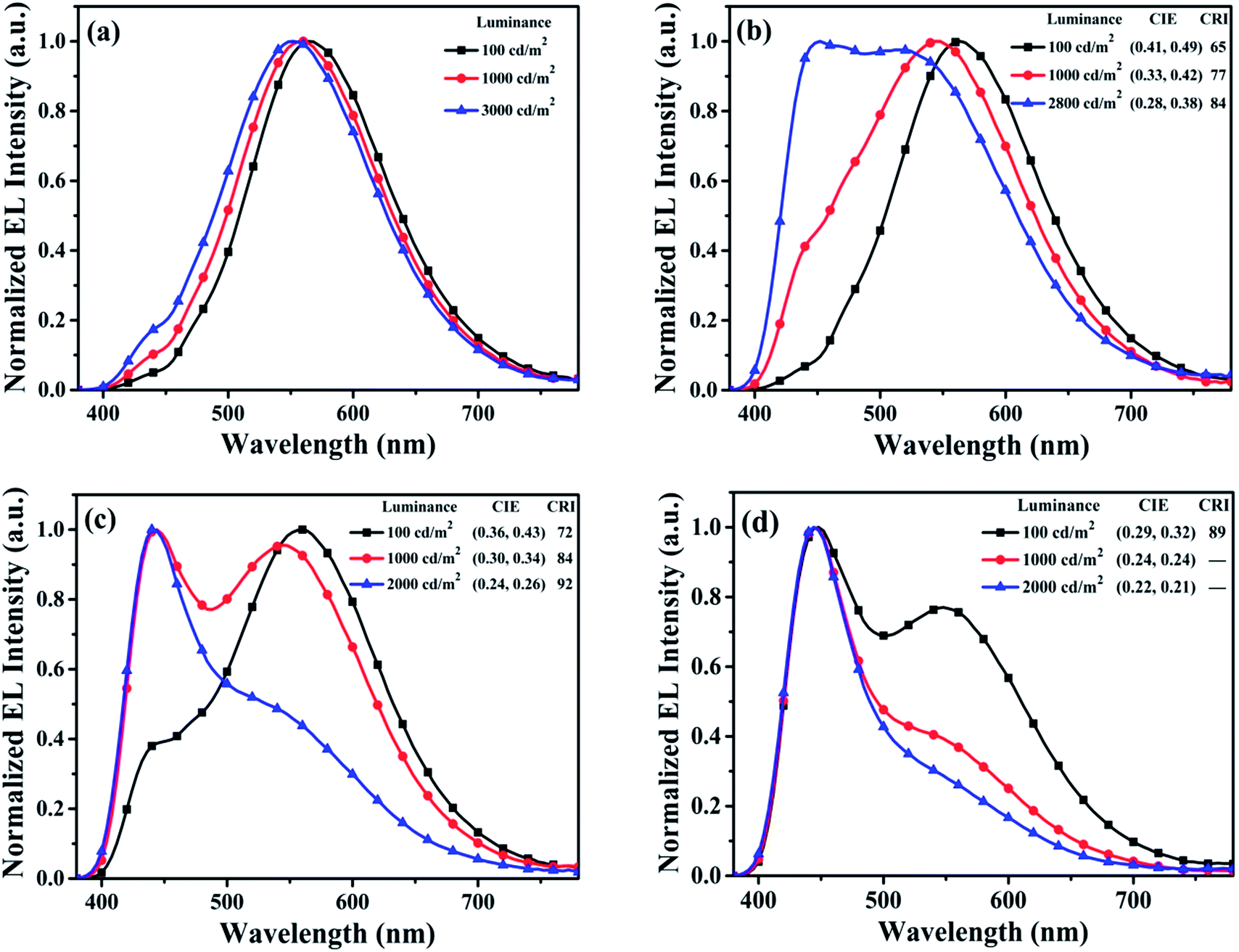 | ||
| Fig. 3 The normalized EL spectra and corresponding CRI of different devices at different luminances, for (a) device Y1, (b) device W1, (c) device W2, and (d) device W3. | ||
From Fig. 3(b)–(d), as 2–4 nm of TCTA CAL is inserted into Bepp2, compared with device Y1, it can clearly be seen that a strong emission peak at about 440 nm appears in the EL spectra of devices W1, W2, and W3, which is typically derived from the emission of Bepp2. This is because some of the electrons are blocked in the TCTA/Bepp2 (46 nm) interface by 2–4 nm of TCTA CAL for blue emission. And it is found that when the thickness of TCTA CAL increases from 2 nm to 4 nm, the emission intensity of Bepp2 becomes stronger in the EL spectra of the corresponding white devices at the same luminance. It is easy to understand that the electron blocking ability for thicker TCTA is further improved and, correspondingly, more electrons will be limited at the TCTA/Bepp2 (46 nm) interface, leading to an enhanced emission intensity of Bepp2.
Along with the appearance of Bepp2 blue emission, combined with the exciplex yellow emission, devices W1, W2, and W3 all realize white emission. For example, at a high luminance of 2800 cd m−2, device W1 obtains a CRI of 84, which has reached the basic requirement for commercial lighting applications (CRI > 80), and is superior to the majority of reported complementary WOLEDs.11,12,29–31,40 Moreover, at a luminance of 2000 cd m−2, device W2 achieves a higher CRI of 92, which, to our knowledge, is the best value among di-chromatic WOLEDs, and even comparable with other reported three-color, four-color, and five-color WOLEDs, as displayed in Table 1.10–31,39,40 However, as the thickness of TCTA further increases to 4 nm, at a luminance of 2000 cd m−2, the corresponding device W3 shows poor color quality due to the yellow intensity almost disappearing in the EL spectra. The CRI value is too low to be measured by a PR655 Spectra scan spectrometer. For devices W1 and W2, such high CRIs are ascribed to (i) the broad-spectrum yellow emission based on the m-MTDATA/Bepp2 exciplex effectively covering more of the visible-light spectral region and greatly enriching the color rendering capability; (ii) the balanced emissions between exciplex yellow light and Bepp2 blue light also boosting the CRI value.
| Structure | EML component | CRImax | References |
|---|---|---|---|
| Exciplex/fluorescent | Blue–yellow | 92 | This work (W2) |
| Exciplex/fluorescent | Blue–yellow | 90 | This work (W5) |
| Fluorescent/fluorescent | Blue–yellow | 84.5 | 40 |
| Fluorescent/phosphorescent | Blue–yellow | 81 | 11 |
| Fluorescent/phosphorescent | Blue–yellow | 81 | 12 |
| Tandem exciplex emitters | Blue–yellow | 70.6 | 29 |
| Exciplex/phosphorescent | Blue–red | 77 | 30 |
| Exciplex/phosphorescent | Blue–red | 90.8 | 31 |
| Exciplex/fluorescent | Blue–green–yellow | 90.2 | 41 |
| Exciplex/phosphorescent | Blue–yellow–red | 85 | 42 |
| Three phosphor-doped emitters | Blue–green–red | 85 | 13 |
| Fluorescent/phosphorescent | Blue–greenish yellow–red | 87 | 14 |
| Four phosphor-doped emitters | Blue–green–orange–red | 94 | 18 |
| Four phosphor-doped emitters | Blue–green–yellow–red | 85 | 21 |
| Fluorescent/phosphorescent | Blue–green–yellow–red | 96 | 22 |
| Fluorescent/phosphorescent | Blue–green–yellow–red | 94 | 24 |
| Fluorescent/phosphorescent | Deep blue–sky blue–green–orange–red | 93 | 26 |
| Fluorescent/phosphorescent | Deep blue–sky blue–green–orange–red | 98 | 27 |
Fig. 4 depicts the J–V and L–V characteristic curves of devices Y1, W1, W2, and W3. Clearly, the introduction of TCTA has a great impact on the EL characteristics of these OLEDs. With the insertion of TCTA and the increase in its thickness, the corresponding device shows an increased turn-on voltage along with a reduced current density and luminance at the same driving voltage, which are caused by the strong electron blocking ability of TCTA. Detailed EL performances of the four devices are shown in Table 2. It can be seen that the maximum luminances for devices W1, W2, and W3 are 2807 cd m−2, 2343 cd m−2, and 2112 cd m−2, respectively, which are obviously below the threshold value (3000–5000 cd m−2) for a WOLED used in lighting applications, limiting their applications in commercial lighting.
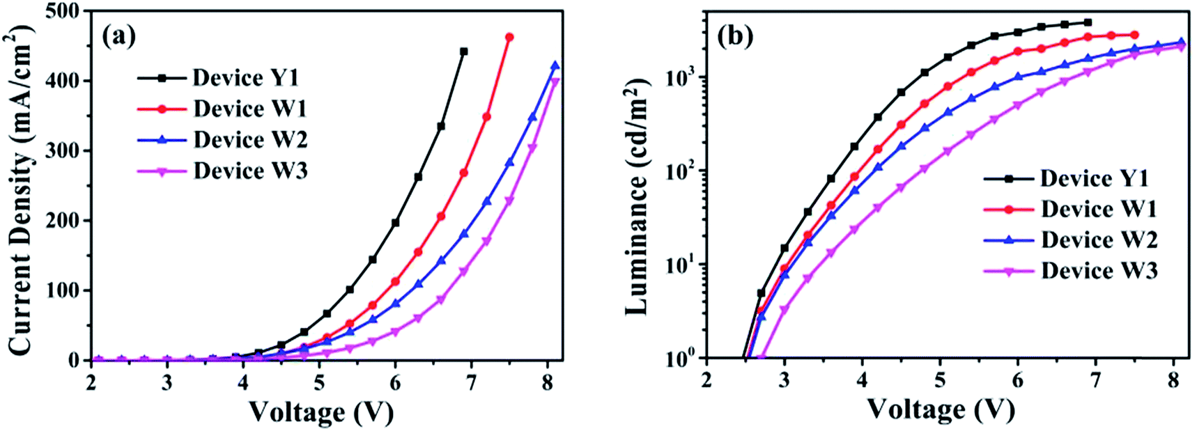 | ||
| Fig. 4 The J–V and L–V characteristic curves of devices Y1, W1, W2, W3, (a) for J–V curve and (b) for L–V curve. | ||
| Device | Vona (V) | Maximum | CIEb | |||
|---|---|---|---|---|---|---|
| Luminance (cd m−2) | CE (cd A−1) | PE (lm W−1) | CRI | |||
| a The turn-on voltage at a luminance of >1 cd m−2.b CIE coordinate at a maximum CRI. | ||||||
| Y1 | 2.4 | 3819 | 5.3 | 6.2 | — | — |
| Y2 | 2.4 | 5983 | 8.5 | 11.1 | — | — |
| W1 | 2.5 | 2807 | 5.2 | 6.1 | 84 | (0.28, 0.34) |
| W2 | 2.6 | 2343 | 4.8 | 5.3 | 92 | (0.26, 0.29) |
| W3 | 2.7 | 2112 | 4.5 | 5.2 | 89 | (0.29, 0.32) |
| W4 | 2.4 | 4215 | 10.5 | 13.7 | 66 | (0.39, 0.47) |
| W5 | 2.5 | 3366 | 8.7 | 10.1 | 90 | (0.28, 0.30) |
| W6 | 3.2 | 3048 | 3.9 | 3.7 | 91 | (0.28, 0.29) |
Generally, the luminance and efficiency of an exciplex formed from a bulk heterojunction are higher than those for one formed from an interfacial heterojunction because the former provides a better contact between the donor and acceptor.43 Inspired by this view, we replaced the m-MTDATA/Bepp2 interfacial heterojunction with a mixed m-MTDATA:Bepp2 bulk heterojunction as the yellow exciplex emitting layer to fabricate a further series of yellow and white devices with the device structure: ITO/m-MTDATA (20 nm)/m-MTDATA:Bepp2 (1:1 5 nm)/TCTA (y nm)/Bepp2 (45 nm)/LiF (1 nm)/Al (100 nm), where y was set as 0, 2, 4, 6, corresponding to devices Y2, W4, W5 and W6, respectively. Detailed device structures and a working mechanism diagram for devices Y2, W4, W5, and W6 are shown in Fig. 5.
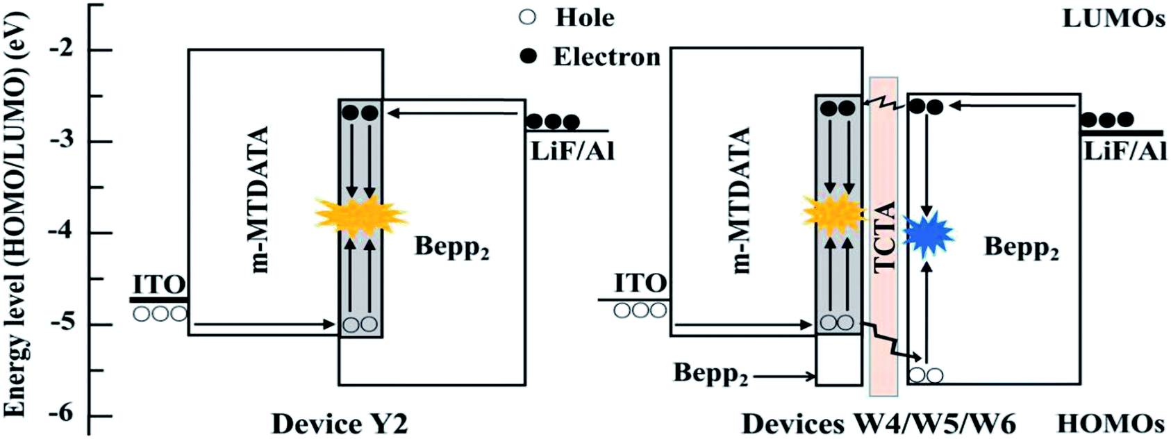 | ||
| Fig. 5 Device structure and working mechanism diagram for devices Y2, W4, W5, and W6. | ||
Fig. 6 shows the normalized EL spectra of the yellow device Y2 and white devices W4, W5, and W6 at luminances of 1000 cd m−2, 2000 cd m−2, and 3000 cd m.−2 From Fig. 6(a), similar to device Y1, we can see that device Y2 with a 5 nm mixed m-MTDATA:Bepp2 layer also emits yellow light with a peak at about 560 nm. But device Y2 shows more stable EL spectra without a blue emission peak from m-MTDATA or Bepp2 over a wide luminance range of 1000–3000 cd m−2, which is attributable to better contact between the m-MTDATA and Bepp2.
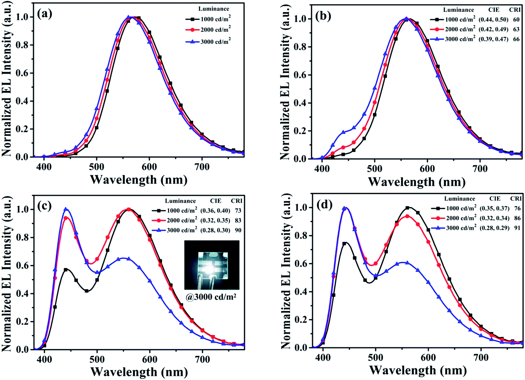 | ||
| Fig. 6 The normalized EL spectra and corresponding CRI of these yellow and white devices at different luminances, for (a) device Y2, (b) device W4, (c) device W5, and (d) device W6. The inset in (c) is a photograph of device W5 under a practical luminance of 3000 cd m−2. | ||
As in the case of devices W1–3, with 2 nm-, 4 nm-, and 6 nm-thick TCTA CALs incorporated into Bepp2, some of the electrons are blocked at the TCTA/Bepp2 (45 nm) interface, causing the blue emission of Bepp2 along with a shoulder located at 440 nm in the EL spectra of devices W4–6, as shown in Fig. 6(b)–(d). However, 2 nm-thick TCTA is too thin to limit a large number of electrons in the TCTA/Bepp2 (45 nm) interface, which causes a weak blue light intensity in the EL spectra of device W4, leading to a poor white emission with a low CRI of 66. As the thickness of TCTA increases to 4 nm and 6 nm, as shown in Fig. 6(c) and (d), the relative intensity of the blue emission is significantly enhanced in the EL spectra of the corresponding devices W5 and W6. As a consequence, high-quality white emission can be anticipated. For example, at a practical luminance of 3000 cd m−2, devices W5 and W6 both achieved extremely high CRIs of 90 and 91, respectively, which both meet the requirement for WOLEDs lighting in hospitals, art galleries, museums, and other special commercial places, etc.22,24
Fig. 7(a) and (b) show the J–V–L and CE–luminance–PE (CE–L–PE) characteristic curves of devices Y2, W4, W5 and W6, respectively, and the detailed EL performances for these devices are also summarized in Table 2. Compared with device Y1, device Y2 with 5 nm of mixed m-MTDATA:Bepp2 layer realizes a dramatically improved luminance and device efficiency, with the maximum luminance, CE, and PE reaching 5983 cd m−2, 8.5 cd A−1, and 11.1 lm W−1, respectively. Correspondingly, compared with the white devices W1–3, the luminance and device efficiency for the white devices W4–6 are also effectively improved, owing to more efficient yellow emission for a 5 nm mixed m-MTDATA:Bepp2 exciplex than an m-MTDATA/Bepp2 interfacial exciplex. The maximum luminance, CE, and PE reach 4215 cd m−2, 10.5 cd A−1, and 13.7 lm W−1 for device W4, 3366 cd m−2, 8.7 cd A−1, and 10.1 lm W−1 for device W5, and 3048 cd m,−2 3.9 cd A−1 and 3.7 lm W−1 for device W6. Interestingly, it is found that the maximum CEs of devices W4 and W5 are higher than that of device Y2, which may be due to the more balanced carrier transport and recombination with the introduction of 2 nm and 4 nm of TCTA. As the thickness of TCTA further increases to 6 nm, the corresponding device W6 exhibits a greatly reduced maximum luminance, CE, and PE, which are also caused by stronger electron blocking ability of 6 nm-thick TCTA.
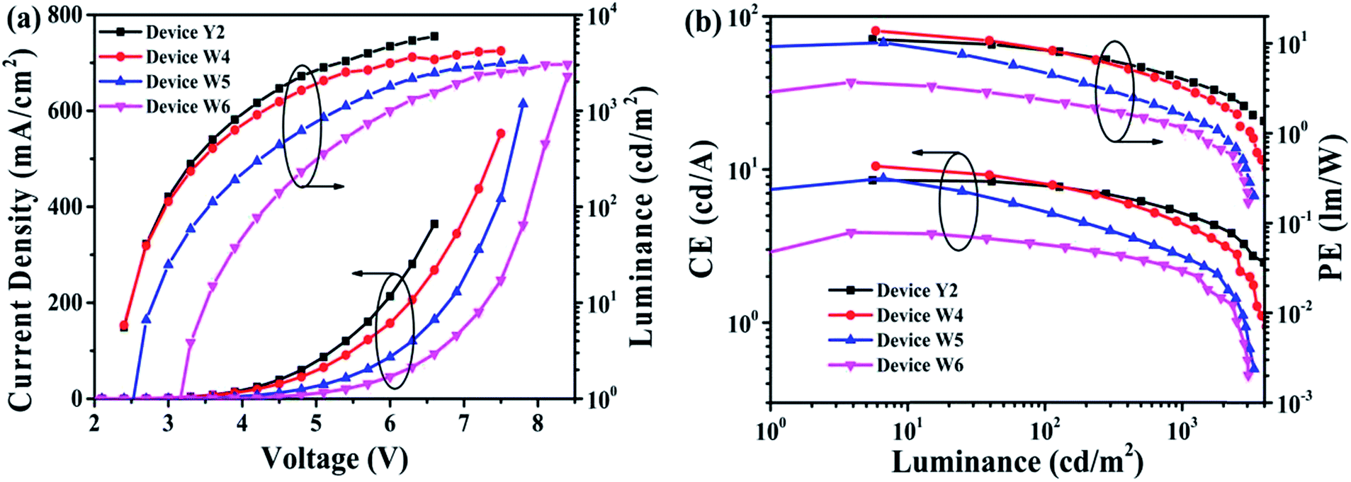 | ||
| Fig. 7 The J–V–L and CE–L–PE characteristic curves of devices Y2, W4, W5, W6, (a) for J–V–L curve and (b) for CE–L–PE curve. | ||
Although ultra-high CRIs (≥90) for devices W2, W5, and W6 were obtained, it is observed that the color stability for devices W1–W6 is relatively poor. For example, as the luminance increases from 100 cd m−2 to 2000 cd m−2, the CIE coordinates for device W2 change from (0.36, 0.43) to (0.24, 0.26); and as the luminance increases from 1000 cd m−2 to 3000 cd m−2, the CIE coordinates for device W5 change from (0.36, 0.40) to (0.28, 0.30). From Fig. 2 and 5, the poor color stability can be easily ascribed to (i) a saturated orange emission from the m-MTDATA/Bepp2 interface exciplex (for devices W1–3) and from the m-MTDATA:Bepp2 exciplex (for devices W4–6) under a high voltage; (ii) an increased blue emission of Bepp2 because more electrons can tunnel the x nm-thick TCTA layer and be transported to the 4 nm-thick bepp2 layer (for devices W1–3) and more holes can overcome the energy barrier of the m-MTDATA/TCTA interface and be transported to the Bepp2 layer (for devices W4–6) under a high voltage.
Here, it is found that the thickness of TCTA CAL plays an important role in the EL spectra of our proposed WOLEDs, which, in turn, will provide a simple method to obtain high-quality white light emission for WOLED lighting applications. It is worth mentioning that compared with other reported ultra-high-CRI WOLEDs which generally suffer from a complicated device structure, high cost and low reproducibility, our proposed white device uses only three organic materials, and both the device structure and the preparation process are fairly simple, which would unlock an excellent method to achieve ultra-high-CRI WOLEDs with low cost, simple structure and good reproducibility, simultaneously.
Conclusions
In conclusion, we employed the exciplex formed between an m-MTDATA donor and a Bepp2 acceptor as a broad-spectrum yellow emitter. By inserting a thin TCTA layer (2–6 nm) as a CAL into the Bepp2 layer of the exciplex, a series of ultra-simple di-chromatic WOLEDs, using only three organic materials, were demonstrated. By changing the thickness of TCTA, the proposed WOLEDs achieve an ultra-high CRI of 92, which, to our knowledge, is by far the simplest structure of complementary WOLEDs with a CRI over 90. In addition, the optimized WOLED, at a practical luminance of 3000 cd m−2, shows an ultra-high CRI of 90, and also realizes high maximum CE and PE of 8.7 cd A−1 and 10.1 lm W−1, respectively. This novel design concept may provide a new avenue for achieving simple-structured, but ultra-high-CRI WOLEDs for various special lighting applications.Conflicts of interest
There are no conflicts to declare.Acknowledgements
The authors gratefully acknowledge the K. C. Wong Education Foundation Hong Kong Baptist University (HKBU) Fellowship Programme for Mainland Visiting Scholars 2017–2018; National Natural Scientific Foundation of China (61705156, 61605137); Shanxi Provincial Key Innovative Research Team in Science and Technology (No. 201605D131045-10); Natural Science Foundation for Shanxi Province (No. 201601D021018, 201601D011031, 2015021028); and Shanxi University Scientific and Technical Innovation Project (No. 2016135, 2015177) for the support of this research.Notes and references
- B. W. D'Andrade and S. R. Forrest, Adv. Mater., 2004, 16, 1585 CrossRef.
- Y. Sun, N. C. Giebink, H. Kanno, B. Ma, M. E. Thompson and S. R. Forrest, Nature, 2006, 440, 908 CrossRef CAS PubMed.
- Z. Liu, L. Zhang, X. Gao, L. Zhang, Q. Zhang and J. Chen, Dyes Pigm., 2016, 127, 155 CrossRef CAS.
- K. T. Kamtekar, A. P. Monkman and M. R. Bryce, Adv. Mater., 2010, 22, 572 CrossRef CAS PubMed.
- Y. Miao, X. Du, H. Wang, H. Liu, H. Jia, B. Xu, Y. Hao, X. Liu, W. Li and W. Huang, RSC Adv., 2015, 5, 4261 RSC.
- K. Wang, Z. Gao, Y. Miao, L. Gao, B. Zhao, H. Xu, Z. Wang, H. Wang and B. Xu, RSC Adv., 2017, 7, 33782 RSC.
- B. Wei, J.-Z. Liu, Y. Zhang, J.-H. Zhang, H.-N. Peng, H.-L. Fan, Y.-B. He and X.-C. Gao, Adv. Funct. Mater., 2010, 20, 2448 CrossRef CAS.
- H. Yang, Y. Shi, Y. Zhao, Y. Meng, W. Hu, J. Hou and S. Liu, Displays, 2008, 29, 327 CrossRef CAS.
- G. Zhou, Q. Wang, C.-L. Ho, W.-Y. Wong, D. Ma and L. Wang, Chem. Commun., 2009, 24, 3574 RSC.
- Y. Miao, Z. Gao, P. Tao, H. Shi, H. Wang, Y. Li, H. Jia, W. Choi and F. Zhu, Sci. Adv. Mater., 2016, 8, 401 CrossRef CAS.
- Y. Miao, B. Zhao, Z. Gao, H. Shi, P. Tao, Y. Wu, K. Wang, H. Wang, B. Xu and F. Zhu, Org. Electron., 2017, 42, 1 CrossRef CAS.
- C.-H. Chang, C.-C. Chen, C.-C. Wu, S.-Y. Chang, J.-Y. Huang and Y. Chi, Org. Electron., 2010, 11, 266 CrossRef CAS.
- Q. Wang, J. Ding, D. Ma, Y. Cheng, L. Wang and F. Wang, Adv. Mater., 2010, 21, 2397 CrossRef.
- J. Yu, Y. Yin, W. Liu, W. Zhang, L. Zhang, W. Xie and H. Zhao, Org. Electron., 2014, 15, 2817 CrossRef CAS.
- Y. Miao, Z. Gao, Y. Li, A. Zhang, H. Wang, Y. Hao, H. Jia, X. Liu and B. Xu, Synth. Met., 2015, 203, 59 CrossRef CAS.
- B. Liu, D. Luo, D. Gao, X. Wang, M. Xu, J. Zou, H. Ning, L. Wang, J. Peng and Y. Cao, Org. Electron., 2015, 27, 29 CrossRef CAS.
- L. Chen, P. Li, Y. Cheng, Z. Xie, L. Wang, X. Jing and F. Wang, Adv. Mater., 2011, 23, 2986 CrossRef CAS PubMed.
- C.-H. Chang, K.-C. Tien, C.-C. Chen, M.-S. Lin, H.-C. Cheng, S.-H. Liu, C.-C. Wu, J.-Y. Hung, Y.-C. Chiu and Y. Chi, Org. Electron., 2010, 11, 412 CrossRef CAS.
- G. Schwartz, M. Pfeiffer, S. Reineke, K. Walzer and K. Leo, Adv. Mater., 2007, 19, 3672 CrossRef CAS.
- Y. Miao, Z. Gao, H. Wang, H. Jia, X. Liu, B. Xu and B. Wei, Org. Electron., 2015, 23, 199 CrossRef CAS.
- Y.-L. Chang, Y. Song, Z. Wang, M. G. Helander, J. Qiu, L. Chai, Z. Liu, G. D. Scholes and Z. Lu, Adv. Funct. Mater., 2013, 23, 705 CrossRef CAS.
- Y. Miao, K. Wang, B. Zhao, L. Gao, P. Tao, X. Liu, Y. Hao, H. Wang, B. Xu and F. Zhu, Nanophotonics, 2017 DOI:10.1515/nanoph-2017-0021.
- X. Zhuang, H. Zhang, K. Ye, Y. Liu and Y. Wang, ACS Appl. Mater. Interfaces, 2016, 8, 11221 CAS.
- N. Sun, Y. Zhao, F. Zhao, Y. Chen, D. Yang, J. Chen and D. Ma, Appl. Phys. Lett., 2014, 105, 013303 CrossRef.
- C.-C. Fan, M.-H. Huang, W.-C. Lin, H.-W. Lin, Y. Chi, H.-F. Meng, T.-C. Chao and M.-R. Tseng, Org. Electron., 2014, 15, 517 CrossRef CAS.
- J.-H. Jou, Y.-C. Chou, S.-M. Shen, M.-H. Wu, P.-S. Wu, C.-R. Lin, R. Z. Wu, S.-H. Chen, M.-K. Wei and C.-W. Wang, J. Mater. Chem., 2011, 21, 18523 RSC.
- J.-H. Jou, S.-M. Shen, C.-R. Lin, Y.-S. Wang, Y.-C. Chou, S.-Z. Chen and Y.-C. Jou, Org. Electron., 2011, 12, 865 CrossRef CAS.
- X. Niu, M. Liang, B. Yao, J. Ding, G. Tu, Z. Xie and L. Wang, Appl. Phys. Lett., 2006, 89, 213508 CrossRef.
- W.-Y. Hung, G.-C. Fang, S.-W. Lin, S.-H. Cheng, K.-T. Wong, T.-Y. Kuo and P.-T. Chou, Sci. Rep., 2014, 4, 1 Search PubMed.
- X.-K. Liu, W. Chen, H. T. Chandran, J. Qing, Z. Chen, X.-H. Zhang and C.-S. Lee, ACS Appl. Mater. Interfaces, 2016, 8, 26135 CAS.
- S. H. Han, J. M. Choi and J. Y. Lee, J. Ind. Eng. Chem., 2016, 46, 49 CrossRef.
- J. Kalinowski, M. Cocchi, D. Virgili, V. Fattori and J. A. G. Williams, Adv. Mater., 2007, 19, 4000 CrossRef CAS.
- D. Luo, Y. Xiao, M. Hao, Y. Zhao, Y. Yang, Y. Gao and B. Liu, Appl. Phys. Lett., 2017, 110, 061105 CrossRef.
- X.-K. Liu, Z. Chan, J. Qing, W.-J. Zhang, B. Wu, H. L. Tam, F. Zhu, X.-H. Zhang and C.-S. Lee, Adv. Mater., 2015, 27, 7079 CrossRef CAS PubMed.
- Z. Chen, X.-K. Liu, C.-J. Zheng, J. Ye, C.-L. Liu, F. Li, X.-M. Ou, C.-S. Lee and X.-H. Zhang, Chem. Mater., 2015, 27, 5206 CrossRef CAS.
- R. Lin, F. Wang, J. Rybicki and M. Wohlgenannt, Phys. Rev. B: Condens. Matter Mater. Phys., 2010, 81, 195214 CrossRef.
- B. Zhao, T. Zhang, B. Chu, W. Li, Z. Su, Y. Luo, R. Li, X. Yan, F. Jin, Y. Gao and H. Wu, Org. Electron., 2015, 17, 15 CrossRef CAS.
- L. Zhang, C. Cai, K. F. Li, H. L. Tam, K. L. Chan and K. W. Cheah, ACS Appl. Mater. Interfaces, 2015, 7, 24983 CAS.
- D. Zhang, M. Cai, Y. Zhang, Z. Bin, D. Zhang and L. Duan, ACS Appl. Mater. Interfaces, 2016, 8, 3825 CAS.
- Y. Miao, Z. Gao, A. Zhang, Y. Li, H. Wang, H. Jia, G. Liu and T. Taiju, Chin. Phys. B, 2015, 24, 057802 CrossRef.
- Y. Hao, W. Meng, H. Xu, H. Wang, X. Liu and B. Xu, Org. Electron., 2011, 12, 136 CrossRef CAS.
- D. Luo, Y. Xiao, M. Hao, Y. Zhao, Y. Yang, Y. Gao and B. Liu, Appl. Phys. Lett., 2017, 110, 061105 CrossRef.
- W.-Y. Hung, G.-C. Fang, Y.-C. Chang, T.-Y. Kuo, P.-T. Chou, S.-W. Lin and K.-T. Wong, ACS Appl. Mater. Interfaces, 2013, 5, 6826 CAS.
| This journal is © The Royal Society of Chemistry 2017 |