
 Open Access Article
 This Open Access Article is licensed under a Creative Commons Attribution-Non Commercial 3.0 Unported Licence
Well protected SmCo nanoclusters: fabrication and transformation to single crystals
Nadeem Abbasab,
Jian-zhong Dingab,
J. Ping Liuabc,
Juan Du ab,
Wei-xing Xiaab,
A-ru Yanab,
Fang Wangd and
Jian Zhang*ab
ab,
Wei-xing Xiaab,
A-ru Yanab,
Fang Wangd and
Jian Zhang*ab
aCAS Key Laboratory of Magnetic Materials and Devices, Ningbo Institute of Materials Technology and Engineering, Chinese Academy of Sciences, Ningbo 315201, China. E-mail: zhangj@nimte.ac.cn
bZhejiang Province Key Laboratory of Magnetic Materials and Application Technology, Ningbo Institute of Materials Technology and Engineering, Chinese Academy of Sciences, Ningbo 315201, China
cDepartment of Physics, University of Texas at Arlington, Arlington, Texas 76019, USA
dNingbo University of Technology, Ningbo, Zhejiang 315211, China
First published on 7th November 2017
Abstract
Highly pure SmCo nanoclusters (NCs) were prepared by a cluster beam deposition (CBD) method. A very thin (<5 nm) protective layer of carbon (C) was used to protect the nanoclusters from oxidation. No oxygen traces were found even after six months, demonstrating that the pure SmCo NCs can be well protected by a thin C protection layer. This result is of significance for the application of high anisotropy rare earth magnetic nanoparticles. Small size NCs experience diffusion-arbitrated coalescence after deposition causing nonuniform size distribution whereas larger clusters show uniform size distribution. Post-annealing SmCo NCs at 500 °C transforms the structure into the single crystal SmCo5 phase with hexagonal CaCu5 symmetry. Higher temperature (≥600 °C) post-annealing causes the structural deterioration of the NCs due to reaction between C and SmCo NCs which is a nanoscale effect and was not observed in bulk counterparts even at 900 °C. The single crystal SmCo5 NCs have potential applications in high density recording media and permanent magnetic materials. In addition, Sm(Co0.7Ni0.3)5 NCs were also prepared. As-produced Sm(Co0.7Ni0.3)5 NCs were amorphous and crystallized at 500 °C. The coercivity of the crystallized Sm(Co0.7Ni0.3)5 NCs was observed as 1820 Oe. These crystallized NCs might be important for scientific as well as future applications.
Introduction
Bulk SmCo5 with a hexagonal CaCu5 crystal structure has the highest magnetic anisotropy constant (1 × 10⁸ ergs per cc) among all magnetic materials,1–3 along with a high curie temperature (1020 K).4 This high anisotropy could be very useful for high density recording media5 if achieved in diminishing size nanoparticles (NPs). An important issue for small size magnetic NPs is the thermal stability. Every magnetic material has a size limit to which it can sustain ferromagnetism. Different materials have a different critical size at a certain temperature. The equation relating anisotropy constant, temperature and size for single domain particles is6| K = 25kT/V | (1) |
![[thin space (1/6-em)]](https://www.rsc.org/images/entities/char_2009.gif) :5 phase) will show superparamagnetism at the lowest critical size. Hence, during the synthesis of SmCo NPs, size control and purity are main obstacles which could affect the magnetic properties. Very fine tuning of different parameters along with ultra-high vacuum (UHV) system is required for the controlled synthesis of desired size and pure SmCo NCs. Use of UHV systems along with high purity processing gases could render synthesis of highly pure SmCo nanostructures, but protection for long time remains an issue because of highly oxidative nature of SmCo. Hence, SmCo must be well protected from oxidation to be used as high anisotropic magnetic material in practical applications. Once it can be protected efficiently then it could be used for various applications. Hence, longer duration protection of small size magnetic NPs is of real interest for basic research as well as application point of view.
:5 phase) will show superparamagnetism at the lowest critical size. Hence, during the synthesis of SmCo NPs, size control and purity are main obstacles which could affect the magnetic properties. Very fine tuning of different parameters along with ultra-high vacuum (UHV) system is required for the controlled synthesis of desired size and pure SmCo NCs. Use of UHV systems along with high purity processing gases could render synthesis of highly pure SmCo nanostructures, but protection for long time remains an issue because of highly oxidative nature of SmCo. Hence, SmCo must be well protected from oxidation to be used as high anisotropic magnetic material in practical applications. Once it can be protected efficiently then it could be used for various applications. Hence, longer duration protection of small size magnetic NPs is of real interest for basic research as well as application point of view.
Crystalline structure promotes anisotropy of the nanostructured SmCo as compared to the corresponding amorphous structure because of magnetocrystalline anisotropy. Various chemical7,8 and physical3,9–12 methods were employed for the synthesis of crystallized SmCo NPs. Chemical methods, have limitations to control size and purity simultaneously. Moreover, synthesis of monodispersed crystalline SmCo NPs less than 20 nm size is still challenging by chemical methods.
Among physical methods, CBD has attracted much attention in the last couple of decades for the synthesis of unique nanostructured materials.13 It has also been used for synthesis of rare earth,9–12 and rare-earth-free magnetic nanoparticles.14–16 Generally, nanostructures were synthesized with CBD technique by optimizing sputtering power, inert gas flow and aggregation length. Sputtering power is driving force in CBD system to obtain desired crystalline structure.9,10,17 Usually, as produced clusters are amorphous so they need crystallization in order to get enhanced magnetic properties. The conversion from amorphous to crystalline structure requires increased thermodynamic conditions which can be achieved either by increasing sputtering power or by annealing. But increase in power has limitations regarding the size of the NCs. Annealing-an alternate choice for crystallization, can be done in two modes-gas phase (pre-deposition/in-flight) and post-deposition modes. Pre-deposition annealing was used to improve crystallinity of SmCo NCs11,12 but this sort of annealing resulted into oxidation.11 In order to use post-annealing for the crystallization of clusters, it is necessary to know the reaction temperature of cover layer (C in our case) with NCs. C is considered not to react with SmCo till 900 °C in the bulk samples so it has been used for cover layer of NPs.3 Considering the fact that materials behave differently at nanoscale, interaction of C with nano-structured SmCo at different annealing temperatures should be explored. Till date no literature reported the structural evolution of single nanocluster with controlled size from the amorphous to the crystalline structure with the annealing temperature. The study of structural transition with annealing temperature for a single nanoparticle is of significance for research, since the transition at nanoscale can be different from bulk. In addition, after exploring the structural transition for single nanoparticle with high anisotropy, the idea can be scaled up for practical applications.
In the present study we emphasize on the, synthesis of very pure SmCo NCs protected with a very thin C layer; size optimization by varying sputtering power and finally conversion of amorphous NCs to single crystal SmCo 1:5 phase by annealing. Reaction of SmCo NCs with C cover layer was studied as a function of temperature which produces some defects at nanoscale in the high temperature regime. Furthermore, synthesis and crystallization of tri-metallic Sm(Co0.7Ni0.3)5 NCs are also discussed briefly.
Experimental setup
We used a composite target of Sm:Co (at% 1:5). High purity Ar (99.9999%) and He (99.9999%) gases were used in the cluster chamber. A linearly adjustable magnetron sputtering based system was used to sputter the target. The base pressure in the deposition chamber was about 5.0 × 10⁻¹⁰ mbar. A highly collimated beam of SmCo NCs comes through a small orifice in the aggregation zone and finally deposits in the deposition chamber on a sample holder kept at room temperature as illustrated schematically in Fig. 1. Deposition rate for clusters was measured in situ by quartz crystal monitor (QCM) to be around 0.15 Å s−1. A similar sputtering gun, installed in deposition chamber, was used to sputter C target, which can be used as a protective layer for the sample. The arrangement is schematically shown in Fig. 1. The deposition rate for C was measured externally by scanning probe microscopy (SPM) and was recorded as 0.51 nm per minute. Both substrate and copper grid were annealed at 500 °C for 10 minutes before deposition of clusters to further clean the surface contaminations.
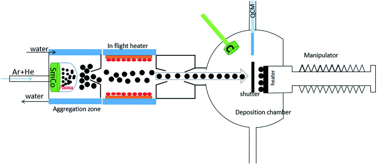 | ||
| Fig. 1 Schematic diagram of CBD [only relevant parts are shown]. | ||
Three types of samples were prepared for the structural evaluation of SmCo NCs. First one with different sputtering powers i.e. 20 W (S1), 33 W (S2) and 43 W (S3) corresponding to sputtering currents-0.15 A, 0.20 A and 0.25 A respectively and second set of samples with different post-annealing temperatures at 400 °C (S4), 500 °C (S5) and 600 °C (S6) each for 10 minutes after the clusters (with the same power as that of S2) were deposited on C coated copper grid. Whereas, a sample (S7) is prepared by using gas phase (in flight) annealing at a heater temperature of 820 °C before the clusters are deposited on the copper grid. Samples from a composite target of Sm(Co0.7Ni0.3)5 were also prepared for TEM and SQUID analysis. C was used as protective layer for all TEM and SQUID samples whereas 100 nm under-layer of Ta was used before depositing NCs on Si substrate. A very thin layer of C (3–5 nm) was used for protection of NCs deposited on copper grid. Higher thickness of carbon was used to protect NCs deposited on Si substrate for SQUID measurements.
Structural evaluation was conducted by transmission electron microscopy Tecnai (TF-20) and (JEOL-2100F) operating at an accelerating voltage of 200 kV with an attached energy dispersive X-ray spectroscopy (EDS). Carbon coated Cu grids were used for the preparation of TEM samples. For TEM measurements NCs were deposited with a low thickness whereas thick films of Sm(Co0.7Ni0.3)5 NCs (about 100) nm were deposited on single crystalline Si (001) substrate for the hysteresis loop measurement. Size distribution was obtained by using Image J and Origin softwares.
Results and discussions
Fig. 2 shows the energy dispersive X-ray spectroscopy (EDS) of the as produced SmCo NCs (sample S2) synthesized by CBD. An area of about 65 × 65 nm2 was selected, particularly for EDS analysis which comprises higher density of NCs. It is vivid from Fig. 2(a) that there was no impurity peak in the sample specifically oxygen contamination was not found. Since rare-earth magnets are prone to oxidation so synthesis of oxygen free nanoclusters has been challenging. The oxidation issue prevents usage of SmCo in various practical applications, despite its high anisotropy. In order to observe whether the sample gets oxidized with time, EDS was repeated for the same sample after six months and we obtained similar results [Fig. 2(b)]. No traces of oxygen were found even after half an year. Additionally, it was perceived that 5 at% carbon (quantitative analysis) is enough to protect SmCo NCs from oxidation. Absence of oxygen contamination in clusters less than 20 nm size, six months after fabrication of SmCo NCs can be very useful for the application point of view as small size NCs are highly demanded for various applications. As SmCo has the highest anisotropy constant so it is very useful for high density recording media, but easy approach to oxidation of this material is an obstruction to be practically used. Herein, we demonstrated that the pure SmCo NCs, oxygen content lower than EDS detection limit, can be synthesized proficiently by CBD method. This triumph could make SmCo NCs practically useable for recording media and other applications. Moreover, it also proves that C is a good protective layer and even very thin layer of C can protect NCs from oxidation and other contamination. Cu and Si peaks in the EDS spectrum are due to Cu grid and background in EDS detector respectively.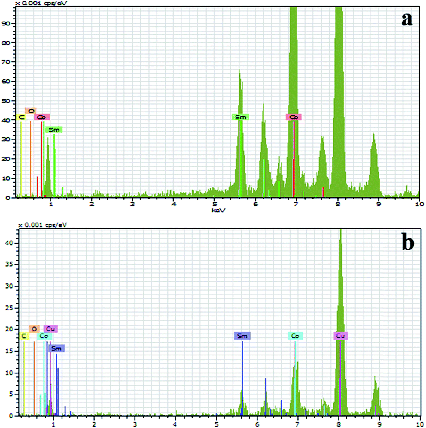 | ||
| Fig. 2 EDS of SmCo NCs. (a) After fabrication (b) six months later. | ||
Fig. 3 illustrates the size, morphology and distribution of NCs at different sputtering powers. Transmission electron microscopy (TEM) images display that NCs have spherical symmetry [Fig. 3(a–c)]. Histograms [Fig. 3(d–f)] show the corresponding size distribution for each sample-S1, S2 and S3 respectively. Statistical data and peak fitting indicates that bimodal sized clusters namely-small and large clusters are formed at low power [Fig. 3(d)]. The size of the small clusters ranges from 7–10 nm and that of large particles is around 27–29 nm. However, there are some clusters with intermediate sizes (10–25 nm) and very few clusters with sizes higher than 30 nm but the frequency of such clusters is very low. The reason for nonuniform size distribution is the coalescence of the clusters, explained in the later part. On the other hand, Fig. 3(b and c) and corresponding histograms [Fig. 3(e and f)] express uniformly distributed clusters following a lognormal distribution with average particle sizes of 13.17 and 17.6 nm with standard deviation of 0.26 and 0.25 for S2 and S3 respectively. The increment in size due to raised sputtering power is similar to other references.10
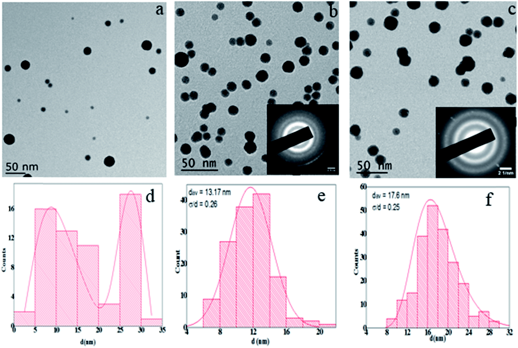 | ||
| Fig. 3 TEM images of NCs at different sputtering powers; (a) S1, (b) S2, (c) S3 and (d), (e) and (f) are histograms of samples S1, S2 and S3 respectively. Insets show SAED patterns of corresponding samples. | ||
From the literature, as prepared SmCo NCs have uniform size distribution3,11,12 but we observed anomalous size distribution of the NCs at low sputtering power as can be seen in Fig. 3(a) so these results are of special interest and need to be discussed. Low sputtering power produces small sized NCs in the aggregation zone, with uniform size distribution, and they are carried to the deposition chamber. Since the cluster growth ceases11 after they exit from the aggregation zone so the only possible reason for the size change of the clusters is some phenomenon after deposition. Possibly, these clusters undergo certain stages of diffusion and finally coalesce. This “diffusion-mediated coalescence” is comparatively slower process18 so initially deposited clusters will have a larger available surface area for their mobility hence they diffuse and coalesce resulting into size enhancement. Whereas the mobility of later deposited clusters will have comparatively less surface area due to presence of already clusters, so they will not coalesce. Moreover, subsequent deposition of C protective layer further limits the mobility of later deposited clusters hence; they can be considered to be pinned to the surface. The size of these pinned clusters remains unchanged. The final size of the clusters depends on number of small clusters coalesced. This phenomenon of cluster growth after deposition is different from the one reported elsewhere19 as a result of Ostwald ripening, in which large clusters grow further at the expense of small clusters. In our case, size of the clusters increases as a result of diffusion-interceded coalescence of two or more small clusters without any shape change.20 Higher sputtering power produces energetically stable NPs so their size remains unchanged consequently giving a uniform size distribution.
In order to check the crystal structure selected area electron diffraction (SAED) was performed. SAED shows broad and diffused ring pattern indicating that clusters are either not crystallized or poorly crystallized [Fig. 3(b) inset]. However, by the increase in power; along with the size increment from 13.17 to 17.6 nm [Fig. 3(c)] the SAED rings also became less diffused and more intense compared to the S2. Some spots could also be observed in the SAED pattern [Fig. 3(c) inset] but still the spots are not sharp so it is obvious that the sample is not crystallized even for this power. This result is consistent with previously reported works that poor crystallinity is observed at this power.17 Further increase in power could convert these amorphous clusters into crystalline structure but it also causes the increase in size10 which is not our focus in this article.
It is well known that the sputtering power, gas flow and aggregation length can be used to tune the size of the NCs in an inert gas condensation system. So we optimized these parameters to get particles of size less than 15 nm. In order to crystallize NCs, first we used in-flight (pre-deposition) annealing from 600–900 °C. TEM in Fig. 4 shows the sample annealed in gas phase at a heater temperature of 820 °C. Diffused and broad SAED pattern [Fig. 4 inset] shows that the particles are not totally crystallized by the gas phase annealing. It can also be observed that clusters just stay on one another after deposition which infers that clusters are energetically stable as their diffusion length is very small. There was also no change observed in particles size under the influence of gas phase annealing. The absence of crystallinity demonstrates that the NCs pass through the heating zone very fast so they are not influenced effectively. The clusters might be crystallized if exposure time of clusters to the heating zone is increased. The above observation suggests to use post-deposition annealing.
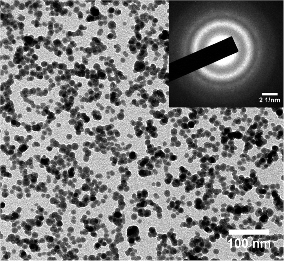 | ||
| Fig. 4 TEM of the sample; in-flight annealed at 820 °C. Inset is corresponding SAED pattern. | ||
High resolution TEM (HRTEM) of the annealed samples is shown in Fig. 5(a–c). Fig. 5(a) demonstrates that at an annealing temperature of 400 °C some regions of the cluster start crystallizing. The marked regions in Fig. 5(a) elucidate crystallization of some parts of the cluster. But it needs higher annealing temperature for complete crystallization. Annealing the sample at a higher temperature of 500 °C for 10 minutes transforms the structure from poor crystalline to single crystal SmCo5 phase with CaCu5 hexagonal symmetry [Fig. 5(b)]. Interplanar distance 0.21 nm corresponds to the high intensity peak (111) of SmCo (1:5) phase.3 The rings in SAED pattern are indexed to SmCo (1:5) phase. The fringe spacing and SAED rings confirms the 1:5 phase of single crystal SmCo NCs. The transformation of SmCo NCs from amorphous to single crystalline structure by using post-annealing in a CBD has not been reported yet. Since, SmCo transforms from 1:5 phase to 2:17 for increased thermal conditions8 so in order to check the behavior of SmCo NCs prepared in our experiment we increased the annealing temperature to 600 °C. A local disorderness in the crystal structure of SmCo NCs was observed at 600 °C as shown in Fig. 5(c). This localized disorderness is attributed to the diffusion of C in localized regions. The diffusion of C dilates the lattice spacing causes deterioration of the structure. It should be noted that clusters might be crystalline as a whole but they will not be single crystal. The weak intensity of corresponding SAED ring (inset Fig. 5(c)) clarifies the disorderness trend at 600 °C. Highlighted region in Fig. 5(d), zoomed image of Fig. 5(c), shows the structural deterioration of the NCs. Furthermore, if the annealing temperature is raised to 650 °C, degree of deterioration increases (results not shown here) showing increased amorphization region of the NCs. Higher is the annealing temperature, more amount of C will diffuse causing increased fraction of disorderness. This diffusion of C into NCs is attributed to nanoscale effect because C does not react with SmCo even at 900 °C in the bulk samples.21 As SmCo (1:5) has high anisotropy and high coercivity so it might be very advantageous for superior ferromagnetic performance, if it could be transformed into single crystal structure. But transformation of SmCo from amorphous to single crystalline structure is challenging due to phase mixing. The complexity further increases at nanolevel because of the interacting nature of magnetic NCs which also turns out to be inhomogeneous size distribution. Hence, the achievement of single crystal SmCo5 NCs, without any shape and size change by post-annealing is of vital importance. The transformation of such small size nanoclusters from as produced amorphous SmCo NCs to single crystal SmCo (1:5) structure by post-annealing have not been reported so far. It is important to note that C is mostly used as capping layer,3,10 since it does not react with SmCo even at 900 °C in the bulk21 but the scenario turns over in nano regime. In our experiment, C reacts with SmCo at temperatures higher than 600 °C. This reaction of C with SmCo NCs at high temperature is nanoscale effect and was not found in the bulk. Usually, SmCo needs high annealing temperature for crystallization but this report about the reaction of C puts a limit for the annealing at nanoscale. It also describes that it is hard to get single crystal SmCo NCs protected with C by means of post-annealing treatment for temperatures higher than 600 °C as C starts to react with SmCo NCs above this temperature. Hence, the choice of appropriate temperature while using C as capping layer is important in order to avoid structural disorderness caused by C diffusion in the lattice at nanoscale. Materials other than C should also be considered for capping while studying the structural evolution of Sm–Co at high annealing temperatures.
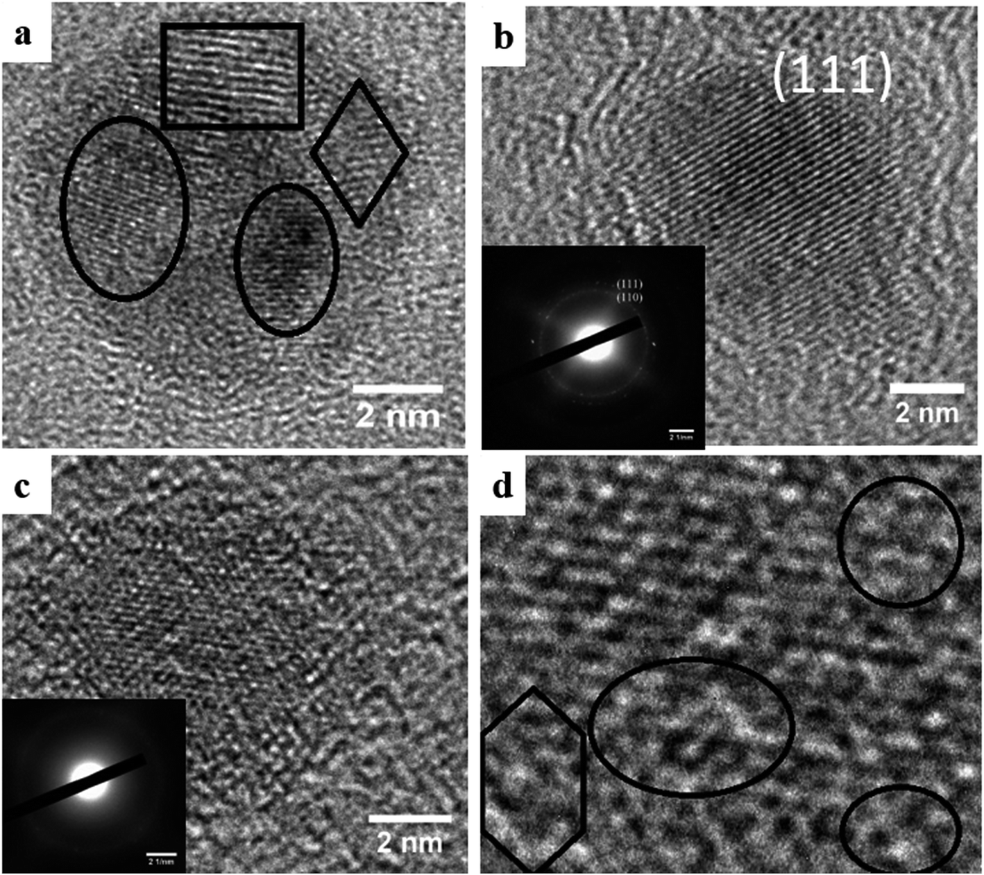 | ||
| Fig. 5 HRTEM of SmCo NCs post-annealed at different temperatures; (a) 400 °C, (b) 500 °C and (c) 600 °C. All samples were annealed for 10 minutes. (d) Zoomed view of (c). | ||
Sm(Co0.7Ni0.3)5 NCs were also prepared and as produced clusters were found amorphous. The clusters transformed to crystallized structure at 500 °C. TEM images of annealed Sm(Co0.7Ni0.3)5 NCs is shown in Fig. 6. Clusters are well separated and spherical in shape. The average size of the clusters is about 13–16 nm. Sharp and well intense diffraction rings in SAED image [inset in Fig. 6(a)] confirms the crystallization of NCs. The SAED rings are indexed to SmCo 1:5 phase. Magnetic properties of the Sm(Co0.7Ni0.3)5 NCs were probed by SQUID measurement. Hysteresis loop of the sample post-annealed at 500 °C is shown in Fig. 6(b). As-produced clusters show very low coercivity of about 180 Oe (not shown) indicating the amorphous nature of Sm(Co0.7Ni0.3)5 NCs. The coercivity of Sm(Co0.7Ni0.3)5 NCs annealed at 500 °C increases to 1820 Oe. This increase in coercivity is attributed to magnetocrystalline anisotropy. The increase in coercivity of annealed sample coincides with TEM observation that Sm(Co0.7Ni0.3)5 NCs were crystallized. This value of coercivity (1820 Oe) is comparable to the values reported for single crystal SmCo5 NCs.9–12 Further investigation on structure and magnetism of Sm(Co0.7Ni0.3)5 NCs is in progress. These crystallized NCs have potential applications in recording media and high performance permanent magnets.
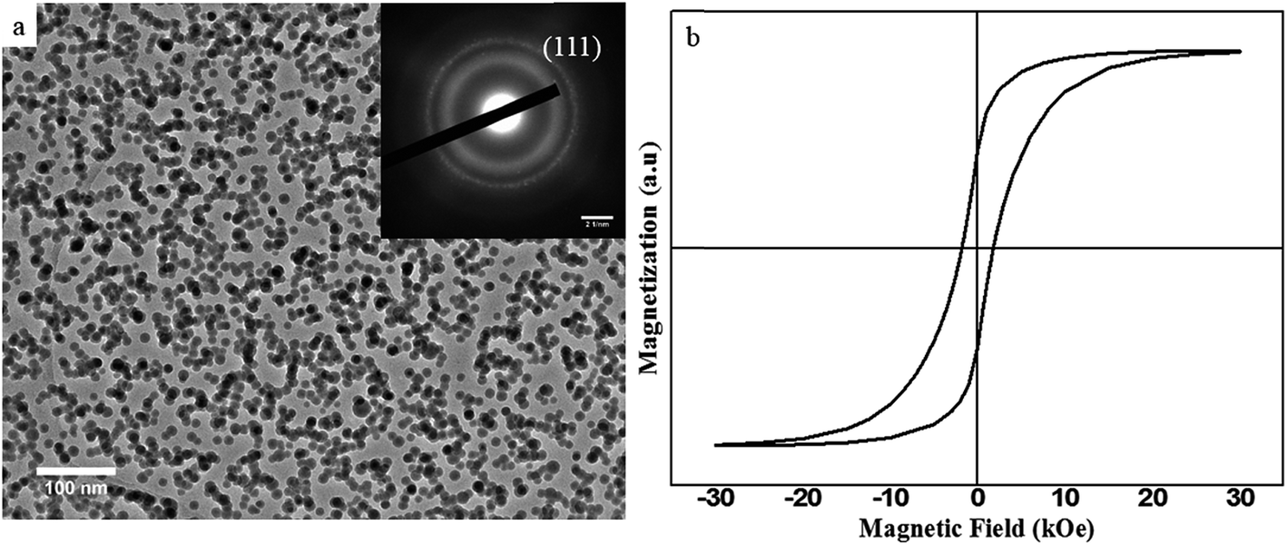 | ||
| Fig. 6 (a) TEM of Sm(Co0.7Ni0.3)5 NCs post-annealed at 500 °C. (b) Room temperature hysteresis loop of the Sm(Co0.7Ni0.3)5 sample annealed at 500 °C. Inset shows SAED pattern for corresponding sample. | ||
Conclusions
In conclusion, we produced very pure Sm–Co NCs, oxygen was too low to be detected by EDS, and the pure Sm–Co NCs can be well protected with a very thin layer of C. We found that for low sputtering power, coalescence of small NCs takes place which results into anomalous size distribution whereas uniform size distribution was observed for higher sputtering power. All as produced samples were amorphous. In-flight annealing applied to crystallize SmCo NCs could not crystallize efficiently because of short exposure time to the heating zone so post deposition annealing was used. Post-annealing treatment showed that amorphous SmCo NCs partially crystallizes at 400 °C and transform to single crystal SmCo 1:5 phase with hexagonal CaCu5 structure at 500 °C. However, further enhancement in annealing temperature causes deterioration of structure leading to unwanted changes in microstructure. This structural change for annealing temperature >600 °C is attributed to the diffusion of C into SmCo NCs. The reaction between C and SmCo NCs at high temperatures post-annealing is nanoscale effect and was not found in corresponding bulk samples even at 900 °C. The coercivity of a film of Sm(Co0.7Ni0.3)5 NCs increases from less than 200 Oe (as deposited NCs) to 1820 Oe for crystalline NCs. The study of crystallized NCs is important for basic research as well as practical applications.
Conflicts of interest
There are no conflicts to declare.Acknowledgements
The authors thank for the support from Chinese National Natural Science Foundation Grant No. 51371185, National Basic Research Program of China Grant No. 2014CB643702, the Program for Key Science and Technology Innovation Team of Zhejiang Province Grant No. 2013TD08, the project of Ningbo Innovative Research Team Grant No. 2012B81001, One Hundred Person Project of the Chinese Academy of Sciences, Research Program of the Chinese Academy of Sciences Grant No. KGCX2-EW-215.References
- F. Liu, Y. Hou and S. Gao, Chem. Soc. Rev., 2014, 43, 8098–8113 RSC.
- M. Yue, J. H. Zuo, W. Q. Liu, W. C. Lv, D. T. Zhang, J. X. Zhang, Z. H. Guo and W. Li, J. Appl. Phys., 2011, 109, 07A711 CrossRef.
- O. Akdogan, W. Li, B. Balasubramanian, D. J. Sellmyer and G. C. Hadjipanayis, Adv. Funct. Mater., 2013, 23, 3262–3267 CrossRef CAS.
- N. Poudyal and J. Ping Liu, J. Phys. D: Appl. Phys., 2013, 46, 043001 CrossRef.
- M. McHenry and D. Laughlin, Acta Mater., 2000, 48, 223–238 CrossRef CAS.
- B. Cullity, Introduction to Magnetic Materials, Addison-Wesley, 1972 Search PubMed.
- C. Yang, L. Jia, S. Wang, C. Gao, D. Shi, Y. Hou and S. Gao, Sci. Rep., 2013, 3, 3542 CrossRef PubMed.
- W. Li, A. Gabay, X. Hu, C. Ni and G. Hadjipanayis, J. Phys. Chem. C, 2013, 117, 10291–10295 CAS.
- B. Balamurugan, R. Skomski, X. Z. Li, G. C. Hadjipanayis and D. J. Sellmyer, J. Appl. Phys., 2012, 111, 07B527 CrossRef.
- G. T. Landi and A. D. d. Santos, J. Mater. Sci., 2010, 45, 4906–4911 CrossRef CAS.
- O. Akdogan, W. Li, G. C. Hadjipanayis and D. J. Sellmyer, J. Nanopart. Res., 2011, 13, 7005–7012 CrossRef CAS.
- S. Stoyanov, V. Skumryev, Y. Zhang, Y. Huang, G. Hadjipanayis and J. Nogués, J. Appl. Phys., 2003, 93, 7592–7594 CrossRef CAS.
- D. J. Sellmyer, B. Balamurugan, B. Das, P. Mukherjee, R. Skomski and G. C. Hadjipanayis, J. Appl. Phys., 2015, 117, 172609 CrossRef.
- B. Balamurugan, B. Das, V. R. Shah, R. Skomski, X. Z. Li and D. J. Sellmyer, Appl. Phys. Lett., 2012, 101, 122407 CrossRef.
- X. Liu, S. He, J.-M. Qiu and J.-P. Wang, Appl. Phys. Lett., 2011, 98, 222507 CrossRef.
- O. Akdogan, W. Li, G. C. Hadjipanayis, R. Skomski and D. J. Sellmyer, J. Appl. Phys., 2012, 111, 07B535 CrossRef.
- S. He, Y. Jing and J.-P. Wang, J. Appl. Phys., 2013, 113, 134310 CrossRef.
- P. Jensen, Rev. Mod. Phys., 1999, 71, 1695 CrossRef CAS.
- X. Wei, R. Zhou, W. Lefebvre, K. He, D. Le Roy, R. Skomski, X. Li, J. E. Shield, M. J. Kramer and S. Chen, Nano Lett., 2014, 14, 1362–1368 CrossRef CAS PubMed.
- W. Fan, X. Gong and W. Lau, Phys. Rev. B, 1999, 60, 10727 CrossRef CAS.
- H. Stadelmaier and N. C. Liu, Chem. Informationsdienst, 1985, 16, 585–588 Search PubMed.
| This journal is © The Royal Society of Chemistry 2017 |