DOI:
10.1039/C7RA10068J
(Paper)
RSC Adv., 2017,
7, 51485-51494
Temperature- and frequency-dependent dielectric response and energy-storage performance in high (100)-oriented Sc doped (Na0.85K0.15)0.5Bi0.5TiO3 films
Received
10th September 2017
, Accepted 21st October 2017
First published on 6th November 2017
Abstract
Highly (100)-oriented (Na0.85K0.15)0.5Bi0.5Ti0.75Sc0.25O3 (NKBT-Sc) films with thicknesses ranging from about 460 to 860 nm were grown by utilizing TiO2 layers engineering. Effects of TiO2 layers on dielectric properties and energy-storage performances of NKBT-Sc films were investigated in a wide temperature range and a wide frequency range. The TiO2 layers inserted alternately inside the NKBT-Sc films can enhance the (100) preferred degree of the film and it doesn't decrease with an increase in film thickness. Compared with NKBT-Sc films without TiO2 layers, the TiO2-coated NKBT-Sc films exhibit a great enhancement in electrical properties and energy-storage performance. The best dielectric properties with the largest dielectric constant (εr) of about 782 and the lowest dielectric loss (tan![[thin space (1/6-em)]](https://www.rsc.org/images/entities/char_2009.gif) δ) of about 0.051 at 1 kHz, together with a maximum energy-density (W) of about 22.7 J cm−3 and corresponding efficiency (η) of about 51.5%, were obtained at room temperature in the 860 nm-thickness film with TiO2 layers coated alternately with NKBT-Sc layers. Moreover, energy-density and the corresponding efficiency of the TiO2-coated NKBT-Sc films varied slightly over a temperature range from −150 °C to 150 °C as well as at a frequency range from 100 Hz to 6 kHz, meaning a greatly enhanced temperature dependent energy-storage stability and a frequency dependent energy-storage stability. In addition, leakage current density (J) of the 860 nm-thickness TiO2-coated NKBT-Sc film was maintained at a relatively low value. This also means that it can work in a wide operating temperature. This much enhanced energy-storage density and good temperature stability make NKBT-Sc films to be a promising lead-free material for energy storage capacitor applications.
δ) of about 0.051 at 1 kHz, together with a maximum energy-density (W) of about 22.7 J cm−3 and corresponding efficiency (η) of about 51.5%, were obtained at room temperature in the 860 nm-thickness film with TiO2 layers coated alternately with NKBT-Sc layers. Moreover, energy-density and the corresponding efficiency of the TiO2-coated NKBT-Sc films varied slightly over a temperature range from −150 °C to 150 °C as well as at a frequency range from 100 Hz to 6 kHz, meaning a greatly enhanced temperature dependent energy-storage stability and a frequency dependent energy-storage stability. In addition, leakage current density (J) of the 860 nm-thickness TiO2-coated NKBT-Sc film was maintained at a relatively low value. This also means that it can work in a wide operating temperature. This much enhanced energy-storage density and good temperature stability make NKBT-Sc films to be a promising lead-free material for energy storage capacitor applications.
1. Introduction
With increasing requirements for compact electronics, ferroelectric thin films have attracted ever-growing interests in recent years due to their practical applications in energy harvesting and storage capacitors.1 The initial ferroelectric material utilized for commercial electronic devices was Pb(Zr,Ti)O3 (PZT)-based owing to its strong electromechanical coupling performance.2,3 Bismuth sodium titanate, (Na0.5Bi0.5)TiO3(NBT) is considered as a potential candidate for such lead-free alternatives due to its strong ferroelectricity plus it undergoes a diffuse phase transition at 320 °C corresponding to its Curie temperature.4 Thus, it was supposed that high energy-storage performance could be realized in NBT-based materials. Nevertheless, it is difficult to obtain desired electrical properties for pure NBT because of its high coercive field and conductivity. Moreover, because a large portion of energy is lost during phase transformation and domain wall motion, it is hard to obtain a high energy storage density for pure NBT.
Solid solutions of NBT with other perovskite-structured compounds have attracted much attention recently because of their greatly enhanced performances due to formation of rhombohedral (R) and tetragonal (T) morphotropic phase boundaries (MPB).5–9 Some efforts have been undertaken to enhance the energy-storage density of NBT-based films. For example, Li et al. obtained a high energy-storage density of about 13.02 J cm−3 and a medium efficiency of about 44.81% in 0.9(Na0.5Bi0.5)TiO3–0.1PbTiO3 thin films due to high electric-field endurance and enhanced polarizability;10 Xu et al. obtained a large energy density of about 36.1 J cm−3 and a corresponding efficiency of about 40.8% in 0.95(Na0.5Bi0.5)TiO3–0.05SrTiO3 thick films.11 In addition, some research progress has been made in the energy-storage field, especially in the active organic energy storage field.12–15 For example, Chi et al. achieved a considerable energy storage density of 7.86 J cm−3 and a much greater η of 58% at 310 kV mm−1 with a 3 vol% 0.5Ba(Zr0.2Ti0.8)O3–0.5(Ba0.7Ca0.3)TiO3 nanofibers (NFs)/PVDF nanocomposite.14 (Na0.5Bi0.5)TiO3-modified K0.5Bi0.5TiO3 (KBT), namely (1 − x)(Na0.5Bi0.5)TiO3–x(K0.5Bi0.5)TiO3, was found to exhibit improved dielectric and piezoelectric properties at the morphotropic phase boundary (MPB) region (x = 0.15) recently.16–21 Our previous research obtained a ferroelectric (remnant polarization Pr of 13.6 μC cm−2, maximum polarization Pmax of 41.2 μC cm−2) and piezoelectric (effective piezoelectric coefficient  of 56 pm V−1) properties in polycrystalline 0.85(Na0.5Bi0.5)TiO3–0.15(K0.5Bi0.5)TiO3 (NKBT) thin films.17 Moreover, it was reported that substitution of an A-site can obtain a relatively higher saturated polarization and/or lower remnant polarization, both of which are beneficial for improving its energy-storage density. Jeon et al. prepared a Mg-doped NBT-KBT thin film with ferroelectric (Pr = 12 μC cm−2, Pmax = 52 μC cm−2) and piezoelectric (
 ) properties by chemical solution deposition.22 According to our research, with an appropriate concentration Sc substitution in a NKBT film, a ferroelectric property (Pr = 18.6 μC cm−2, Pmax = 57.4 μC cm−2) and piezoelectric property (
 ) were obtained.23
Electrical properties of a ferroelectric thin film depend heavily on its structural properties, in which orientation of crystalline phase and film–substrate interfacial structure are important factors that need to be considered. It was reported that by introducing a buffer layer, a highly oriented crystallized perovskite thin film can be obtained, which was expected to perform with electrical properties better than those of polycrystalline thin films. For example, Xie et al. reported that a highly (100)-oriented 0.4Bi(Ni0.5Zr0.5)O3–0.6PbTiO3 film was prepared through alternately introducing PbO layers, in which an increased back-switching behavior (Pmax − Pr) process and decreased coercive field (Ec) were obtained;24 Chi et al. obtained a greatly improved polarization performance (Pr = 14.6 μC cm−2, Pmax = 74.2 μC cm−2) in high-quality (100)-orientated NKBT thin film by using a LaNiO3 layer.25
Li et al. found that a TiO2 layer could induce highly preferred orientation in Bi3.15Nd0.85Ti3O12 and improved dielectric and ferroelectric performances.26 Aoki et al. reported that a thin TiO2 layer could lower the crystallization temperature of a PZT thin film and modified its properties.27 Therefore, it can be predicated that a possibility of enhancing energy-storage performance can be obtained by deliberately engineering TiO2 layers. The aim of this work was to explore the possibility of enhancing energy storage density in Sc-doped NKBT [(Na0.85K0.15)0.5Bi0.5Ti0.75Sc0.25O3 (NKBT-Sc)] films by deliberately engineering TiO2 layer effects. Dielectric, ferroelectric, and corresponding energy storage properties of TiO2-coated films were systematically investigated in an operating temperature range from −150 °C to 150 °C and a frequency range from 100 Hz to 6 kHz.
2. Experimental procedure
2.1. Material synthesis
The NKBT-Sc films film-capacitors were prepared by aqueous sol–gel processing. As for the NKBT films, bismuth nitrate [Bi(NO3)3·5H2O], tetrabutyl titanate [Ti(OC4H9)4], sodium acetate [NaCOOCH3], potassium acetate [KCOOCH3], and scandium acetate [Sc(COOCH3)3] were used as precursor materials with glacial acetic acid, isopropyl alcohol, and distilled water as the solvents. First, Ti(OC4H9)4, isopropyl alcohol, and acetylacetone with a weight ratio of 1:3:3 were mixed. Subsequently, glacial acetic acid in a 3:1 volume ratio was poured into the mixture. Then, Bi(NO)3, with an amount according to the composition of (Na0.85K0.15)0.5Bi0.5Ti0.75Sc0.25O3, was dissolved in the solution, and in the meantime distilled water of the same volume as the glacial acid was added. Finally, NaCOOCH3 and KCOOCH3 and Sc(COOCH3)3 according to the (Na0.85K0.15)0.5Bi0.5Ti0.75Sc0.25O3 composition, were dissolved into the solution one by one. To prevent the appearance of cracks during aging and drying steps, an appropriate formamide (about 10:1 in volume ratio) was added to the above solution as a stabilizing agent.5 During the whole preparation process, the mixture was stirred constantly at room temperature until a transparent and stable yellow solution with a concentration of 0.26 M, determined by an inductive coupled plasma emission spectrometer (ICP), was obtained. In the preparation, ten percent excess of bismuth and twenty percent excess of sodium/potassium was added to balance out their volatility during the heat treatment process. The resultant solution was aged for about ten days before deposition. The organic solution for the TiO2 layer was prepared by dissolving tetrabutyl titanate [Ti(OC4H9)4] into the solvent with mixed glacial acetic acid and isopropyl alcohol (weight ratio of 1:1) under constant stirring. Then, an appropriate formamide (about 10:1 in volume ratio) was added to the above solution forming a stable precursor sol. The resultant solution, with a concentration of 0.02 M determined by ICP, was aged for about ten days before deposition.
The Ti-containing solution was spin-coated deposited on Pt/Ti/SiO2/Si followed by sequentially drying at 100 °C for 10 min and pyrolyzing at 400 °C for 5 min, forming a thin TiO2 layer. Fig. 1 shows the XRD pattern of the crystallized TiO2 layer on the substrate. The peak at about 2θ = 48° corresponds to the (200) orientation of anatase phase TiO2. (JCPDS [Joint Committee on Powder Diffraction Standards] 89-4921). The inset shows the SEM surface morphology of the crystallized TiO2 layer, in which isolated fine nanocrystals are sparsely distributed on the Pt electrode. Then, a NKBT-Sc layer was deposited on the TiO2-coated substrate by spin coating at 4500 rpm for 30 s, followed by drying at 100 °C for 10 min and pyrolyzing at 450 °C for 5 min. After three NKBT-Sc layers were deposited, then another TiO2 seeding layer was deposited onto the as-prepared NKBT-Sc film; i.e., the films were prepared by depositing one TiO2 layer and three NKBT-Sc layers alternately, forming a sandwich multilayer structured film. This processing was repeated for various times to obtain different thicknesses. For comparison, the NKBT-Sc film with one TiO2 layer inserted at the film–electrode interface and one without the TiO2 layer were also prepared. Finally, all the film samples were annealed at 700 °C for 5 min in a rapid thermal processing furnace. For characterizing the electric properties, top electrodes of platinum with a diameter of 0.2 mm were sputter-deposited onto the surface of the films. For ease of description, the NKBT-Sc film without a TiO2 layer, the NKBT-Sc film with a TiO2 seeding layer only at the film–electrode interface, and the film with alternate TiO2 seeding layers are denoted as NKBT-Sc-a, NKBT-Sc-b, and NKBT-Sc-c, respectively. A schematic drawing of the three kinds of structured films is shown in Fig. 2.
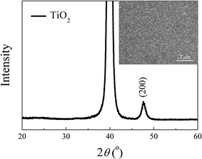 |
| | Fig. 1 XRD pattern of the TiO2 layer on Pt/Ti/SiO2/S. The inset shows SEM surface morphology of the TiO2 layer on Pt/Ti/SiO2/Si. | |
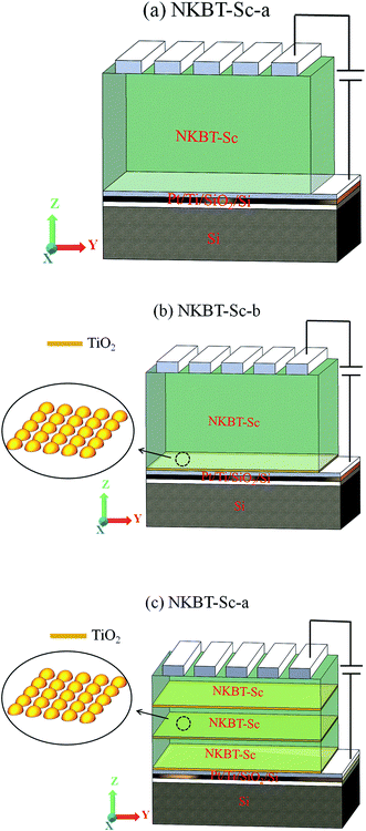 |
| | Fig. 2 Schematic drawing of the three kind of structured films: (a) NKBT-Sc-a, (b) NKBT-Sc-b, and (c) NKBT-Sc-c. | |
2.2. Material characterization
The phase composition of the prepared films was characterized by θ–2θ scan X-ray diffraction (XRD, D/max-RB, Rigaku, Tokyo, Japan) with CuKα radiation. Surface microstructure of the films was observed by field-emission scanning electron microscopy (FE-SEM, Hitachi-S4800, Hitachi, Japan). The ferroelectric hysteresis loops and dielectric properties were measured by a ferroelectric test module (TF 2000 analyzer, axiACCT, Aachen, Germany) and a precision impedance analyzer (4294A, Agilent, USA), respectively. Temperature was controlled by a temperature control stage (THMS600, Guildford, UK.).
3. Results and discussion
3.1. Crystallographic orientation and microstructure
Fig. 3 shows XRD patterns of NKBT-Sc-a, NKBT-Sc-b, and NKBT-Sc-c with the NKBT-Sc thicknesses of about 460 and 860 nm, respectively. All the films grow in a pure-phase perovskite structure with no detectable impurity or other phases. The NKBT-Sc-a films are all randomly oriented with the (110) diffraction peak showing the highest intensity, and which is independent of film thickness. With the insertion of a TiO2 layer, the NKBT-Sc-b and NKBT-Sc-c films are (100) oriented, and in the meantime, the full width at half maximum (FWHM) of the (100) diffraction peak decreases, indicating a rise of crystallization degree. Because of close “in-plane” lattice parameters (0.352 nm) of anatase TiO2 with a-axis lattice parameters (0.381 nm) of NKBT,28–30 TiO2 can provide nucleation sites to assist the (100)-oriented growth of the films, since lower interface energy promotes nucleation of grains. This can mostly be contributed to the formation of (100)-preferred orientation and better crystallinity of the films. As for the NKBT-Sc-b film, the degree of (100)-preferred orientation decreases with increasing film thickness. When the TiO2 seeds are coated inside NKBT-Sc films, the obtained NKBT-Sc-c film exhibits a larger degree of (100)-preferred orientation than that of the NKBT-Sc-b films, and it does not decrease as the thickness increases. The TiO2 layer inserted at the film–electrode interface has a weaker effect on the upper part of the as-deposited NKBT-Sc film, which accordingly causes a lower degree of (100) orientation as the film thickness increases. Furthermore, TiO2 layers inserted inside the films can also act as seeds and play a role of nucleation, which further enhances (100)-preferred degree and facilitates the crystallization process. The degree of (100) orientation (D(100)) is analyzed by calculating the peak integrated intensity ratio of (100) relative to the sum of (100), (110), and (111),31 and the results are given in Fig. 3.
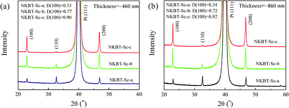 |
| | Fig. 3 XRD patterns of the three kinds of NKBT-Sc films with thicknesses of about (a) 460 nm and (b) 860 nm. | |
Surface morphologies of the films are measured by FE-SEM. Fig. 4(a)–(c) show surface SEM images of the NKBT-Sc-a, NKBT-Sc-b, and NKBT-Sc-c films with about 860 nm thickness, respectively. These three kinds of NKBT-Sc films exhibit a dense morphology with uniform grain size distribution. Furthermore, the TiO2-coated NKBT-Sc films exhibit a larger mean grain size than the ones without a TiO2 layer. Transmission electron microscope (TEM, F20, Tecnai) was used to further study the microstructure and Fig. 4(d) shows the TEM image of the 860 nm-thickness NKBT-Sc-c film at the region of the NKBT-Sc film–TO2 interface. Although there are some dislocations observed at the interface due to a slight lattice mismatch, a clear interface and, moreover, some consecutive lattice images at the interface are presented. In addition, according to the observation of the selected area electron diffraction (SAED) image, a highly preferred orientation exists in the NKBT-Sc film.
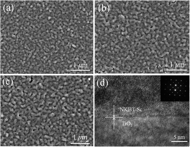 |
| | Fig. 4 SEM surface images of the (a) NKBT-Sc-a, (b) NKBT-Sc-b, and (c) NKBT-Sc-c films with thicknesses of about 860 nm; (d) TEM image of the 860 nm-thickness NKBT-Sc-c film. | |
3.2. Electrical properties and energy storage performance
DC-applied field dependent dielectric constants (εr) and dissipation factors (tanδ) of these three kinds of NKBT-Sc films were measured under a small oscillation signal at 1 kHz, as shown in Fig. 5(a). The butterfly shape of the dielectric constant DC-applied field curve confirms the ferroelectric characteristics of the three kinds of NKBT-Sc films. According to the testing data, the εr and tanδ of these three kinds of films, with thicknesses of about 460 nm and 860 nm at 0 and 1200 kV cm−1, are listed in Table 1. Throughout the range of the DC bias field, the TiO2-coated NKBT-Sc films show better dielectric properties than the film without a TiO2 layer. The 860 nm-thickness NKBT-Sc-c film exhibits the largest εr of about 782 and lowest tanδ of 0.051, while the NKBT-Sc-a film with the same thickness exhibits the lowest εr of about 563 and largest tanδ of about 0.077. The improved dielectric properties for the NKBT-Sc-c and NKBT-Sc-b films can be attributed to the following: first, TiO2 seeds (PbO nanocrystals) on the surface of substrates and inside films can induce the high (100)-preferred orientation, which can improve domain-wall mobility. Second, the better crystallinity and consequently larger mean grain size in the highly (100)-oriented NKBT-Sc films can decrease the pinning-effect of the defects. Besides, for any of these three structures, the 860 nm-thickness film exhibits a better dielectric property than the 460 nm-thickness film. The higher (100)-preferred orientation for the thicker NKBT-Sc-b film, and better crystallinity for the thicker NKBT-Sc-a and NKBT-Sc-c can be considered as the main reasons to cause the enhanced dielectric response. In addition, it is observed that differences of the εr value gradually decrease with increasing DC applied field and tend to become insignificant among these films at a high DC-applied field. It is well known that the dielectric response includes intrinsic contributions and extrinsic contributions. DC-applied field-dependent dielectric properties come from combined contributions of field-dependent intrinsic dielectric permittivity and extrinsic dielectric permittivity. At high DC-applied fields, extrinsic contributions, which mainly originate from domain wall motion, tend to be pinned, thus dielectric response mostly arises from intrinsic contributions of the film. This indicates that the improved dielectric constant after the insertion of a TiO2 layer at zero DC applied field is mainly attributed to an extrinsic contribution, i.e., motion of domain walls. By inserting a TiO2 seed layer at the film–electrode interface and inside films, the high (100) orientation and better crystallinity can depress the pinning-effect of the charged defects and thus enhance domain-wall mobility. This may be the main reason causing the enhanced dielectric properties of the NKBT-Sc-b and NKBT-Sc-c films. In addition, lowered dielectric loss in the TiO2-coated NKBT-Sc films compared with the NKBT-Sc-a film can be attributed to the rise of crystallization degree. Since the pinning-effect of the defects will weaken gradually with increasing AC field, more domain walls contribute to the dielectric permittivity at larger AC fields, which can be characterized by the Rayleigh relation. Fig. 5(b)–(d) show the AC field-dependent amplitude of the normalized dielectric constant, measured at −150 °C, 20 °C, and 150 °C, respectively. The dielectric constants increase linearly with increasing AC field, conforming to the Rayleigh relation.32 The Rayleigh coefficient, which is calculated according to the slope of the curves, is used to represent the contribution from a pinned domain wall and a larger Rayleigh coefficient means more contribution from domain walls in the films. The NKBT-Sc-b and NKBT-Sc-c films exhibit a larger Rayleigh coefficient than the NKBT-Sc-a film, meaning more domain walls contribute to the dielectric response at a large AC field. Higher domain wall mobility can be ascribed to better crystallization quality and a higher degree of (100)-preferred orientation. When measuring at a temperature range from 20 °C to −150 °C, the dielectric constant decreases gradually, and in the meantime the dielectric constant differences between the three kinds of films become smaller. Because the motion of a pinned domain wall is a thermally activated process, which will gradually diminish as the measurement temperature decreases, fewer domain walls contribute to the dielectric response at low measurement temperatures.
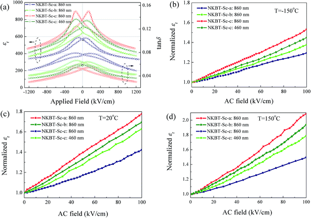 |
| | Fig. 5 (a) Applied voltage-dependent dielectric constant εr and dielectric loss tanδ of the three kinds of NKBT-Sc films; AC field-dependent normalized dielectric constant measured at (b) −150 °C, (c) 20 °C, and (d) 150 °C. | |
Table 1 The εr and tanδ of the three kinds of NKBT-Sc films with thicknesses of about 460 nm and 860 nm at DC applied fields of 0 and 1200 kV cm−1
| Sample |
NKBT-Sc-a |
NKBT-Sc-b |
NKBT-Sc-c |
| 460 nm |
860 nm |
460 nm |
860 nm |
460 nm |
860 nm |
| 0 kV cm−1 |
| εr |
487 |
563 |
617 |
687 |
725 |
782 |
| tanδ |
0.079 |
0.077 |
0.068 |
0.063 |
0.058 |
0.051 |
|
| 1200 kV cm−1 |
| εr |
307 |
343 |
342 |
387 |
418 |
463 |
| tanδ |
0.053 |
0.047 |
0.043 |
0.041 |
0.038 |
0.034 |
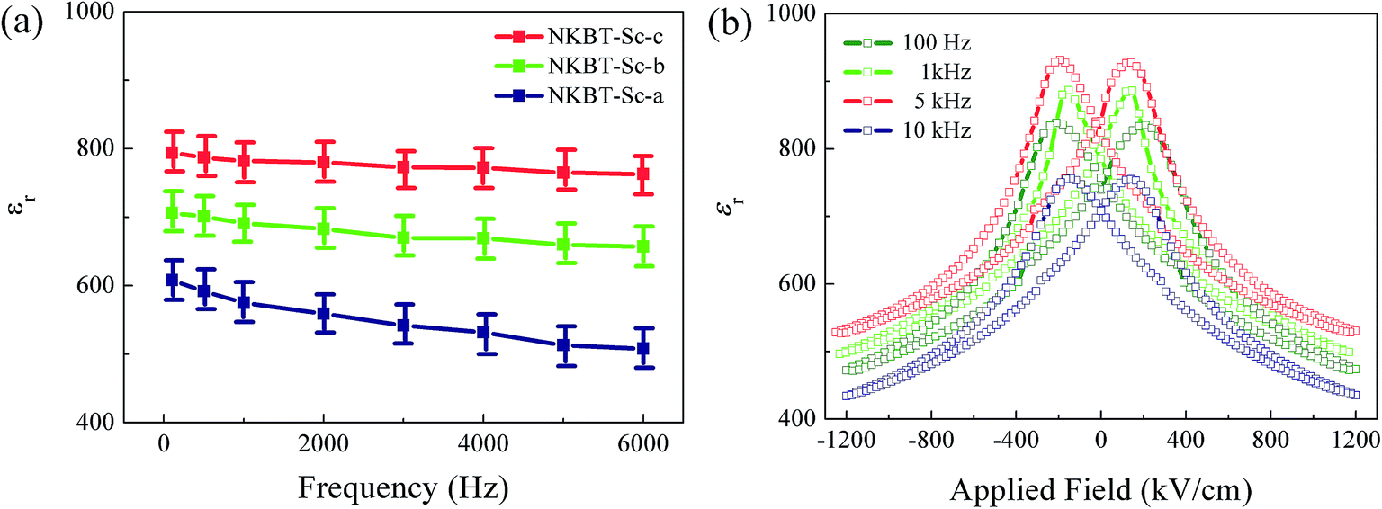
The dielectric constants of these three kinds of 860 nm-thickness NKBT-Sc film were also measured at a frequency range of 100 Hz to 6 kHz, as shown in Fig. 6(a), and the corresponding applied field-dependent dielectric constants of the 860 nm-thickness NKBT-Sc-c film measured at different frequencies are shown in Fig. 6(b). When measuring at a frequency from 100 Hz to 6 kHz, the εr values of the NKBT-Sc-b and NKBT-Sc-c films decline slightly, while those values of the NKBT-Sc-a film were found to decrease more obviously. This indicates that the TiO2-coated NKBT-Sc films are less frequency sensitive than those without a TiO2 layer under the same measurement conditions.
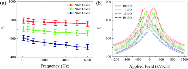 |
| | Fig. 6 (a) Dielectric constants of these three kinds of 860 nm-thickness NKBT-Sc films measured at a frequency range of 100 Hz to 6 kHz. (b) Corresponding applied field-dependent dielectric constants of the 860 nm-thickness NKBT-Sc-c film measured at different frequencies. | |
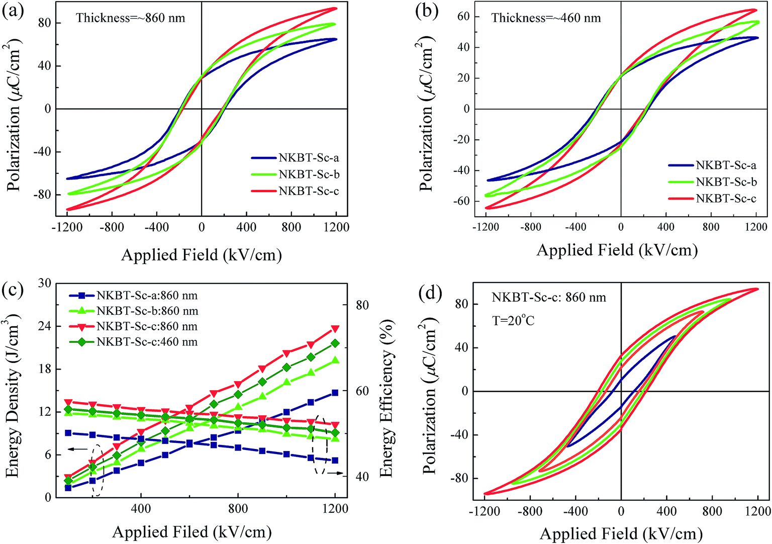
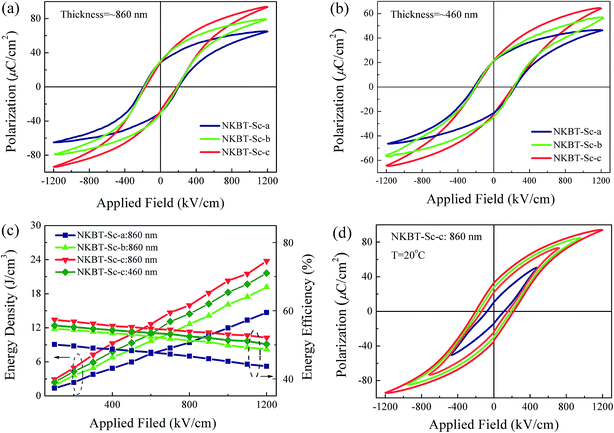
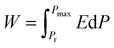
For studying ferroelectric properties, polarization-applied field hysteresis loops with sequentially increasing applied fields were measured for these three kinds of NKBT-Sc films at 1 kHz. The applied field dependent hysteresis loops of the three kinds of NKBT-Sc films with thicknesses of about 860 nm and 460 nm measured at room temperature are shown in Fig. 7(a) and (b), respectively. All the films exhibit slim P–E loops at high electric-fields, meaning a high electric-field endurance. The insertion of a TiO2 layer exerts a positive impact on the Pmax value but nearly no effect on the Pr of these films. This can be attributed to the TiO2 layer effect by motivating more domain response to and orienting along the external field direction. Besides, a larger spontaneous polarization exists along the (100) orientation than that along the (110) orientation. Thus, with the insertion of a TiO2 layer, the highly (100)-oriented NKBT-Sc film exhibits a higher ferroelectric response than the polycrystalline one. Grain boundaries and interfacial defects are generally considered as a potent leakage current path. The larger mean grain size in the TiO2-coated films results in a decreased current path, which lowers density of charged defects gathered at the NKBT-Sc film–TiO2 interfaces and thus causes reduction of the pinning-effect of the charged defects. However, once the applied field is removed, those polar domains tend to switch to their original random polarized state, and this increases a back-switching behavior (Pmax − Pr) process. Energy storage density W ( ), energy loss Wloss and energy efficiency η (η = W/(W + Wloss)) in dielectric capacitors can be calculated from the P–E loops.33,34 Ferroelectric materials with higher dielectric breakdown strength (BDS) and larger differences between Pmax and Pr have the potential to be applied in electronic devices and systems such as high energy-storage capacitors. Fig. 7(c) depicts the applied field dependent energy density and efficiency of these three kinds of NKBT-Sc films. According to the calculated results, the energy density W and energy efficiency η of these three kinds of films, with thicknesses of about 460 nm and 860 nm at 1200 kV cm−1, are listed in Table 2. The P–E loops of the 860 nm-thickness NKBT-Sc-c film measured at room temperature under different electric fields are shown in Fig. 7(d). The energy storage density W of these three kinds of NKBT-Sc films are found to increase almost linearly with increasing applied field, while in the meantime the energy efficiency η shows an opposite tendency. The TiO2 layer has a strong impact on energy-storage performance and moreover this performance greatly enlarges by deliberately engineering a strong TiO2 layer. The 860 nm-thickness NKBT-Sc-c film exhibits the best energy-storage performance among the three kinds of NKBT films with a W value of about 22.7 J cm−3 and an efficiency η of about 51.5%, while the 860 nm-thickness NKBT-Sc-a film showed a W value of about 12.3 J cm−3 and η value of about 43.7% at 1200 kV cm−1. In addition, the thicker TiO2-coated NKBT-Sc films (860 nm-thickness) exhibit a higher W value together with a lower η value than the 460 nm-thickness ones. Energy density obtained at a low applied field in the TiO2-coated NKBT-Sc films in this work is superior to the values reported for NBT-based ceramics.35–37
 |
| | Fig. 7 (a) Applied field-dependent hysteresis loops of the three kinds of NKBT-Sc films measured at room temperature with thicknesses of about (a) 860 nm and (b) 460 nm. (c) Applied field dependent energy density and efficiency of the three kinds of NKBT-Sc films. (d) Applied field-dependent hysteresis loops of the 860 nm-thickness NKBT-Sc-c film measured at room temperature under different electric fields. | |
Table 2 The energy density W and energy efficiency η of the three kinds of NKBT-Sc films with thicknesses of about 460 nm and 860 nm at 1200 kV cm−1
| Sample |
NKBT-Sc-a |
NKBT-Sc-b |
NKBT-Sc-c |
| 460 nm |
860 nm |
460 nm |
860 nm |
460 nm |
860 nm |
| W (J cm−3) |
10.8 |
12.3 |
16.2 |
18.4 |
20.5 |
22.7 |
| η |
41.2% |
43.7% |
47.3% |
48.7% |
50.6% |
51.5% |
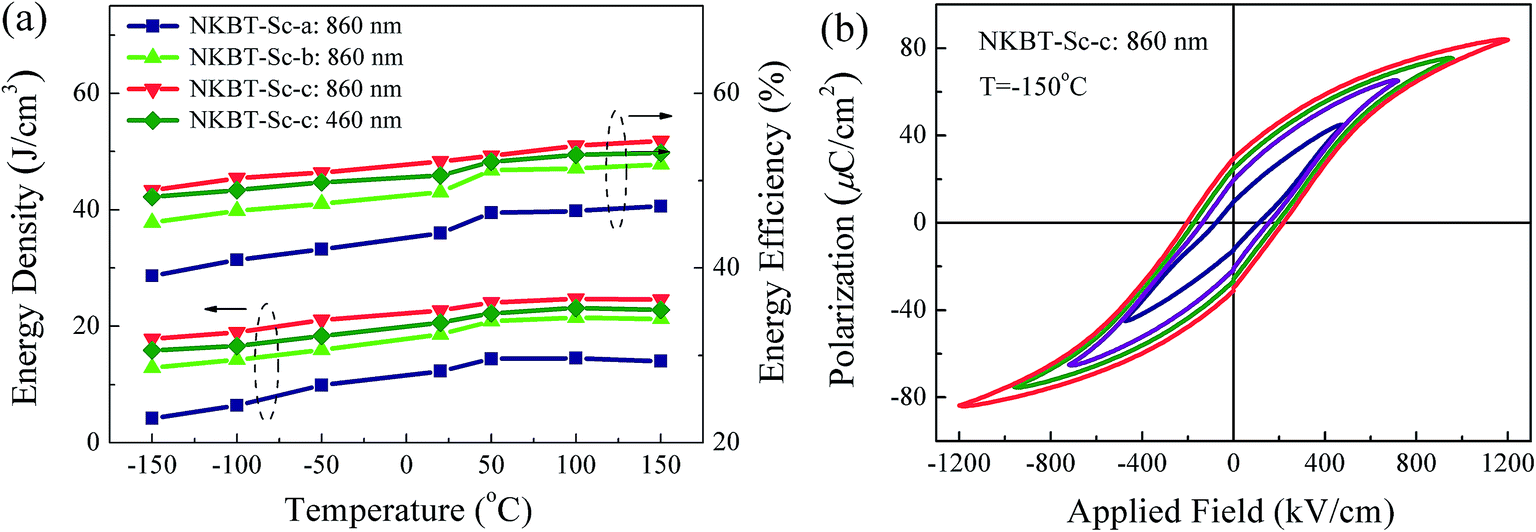
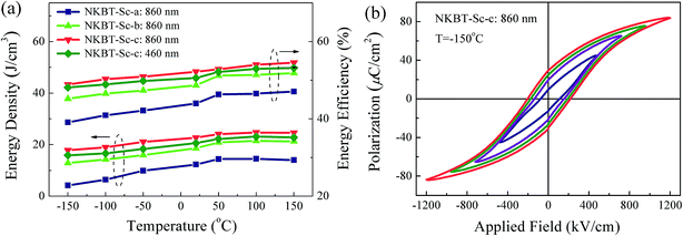
As temperature stability of energy-storage performance is crucial for practical applications of capacitors, the temperature dependent energy storage performance of these three kinds of NKBT-Sc films was measured at a temperature range from −150 to 150 °C at 1200 kV cm−1, and the result is shown in Fig. 8(a). Fig. 8(b) shows the corresponding P–E loops of the 860 nm-thickness NKBT-Sc-c film under different electric fields measured at −150 °C. With the insertion of a TiO2 layer, the NKBT-Sc-b and NKBT-Sc-c films display a slight fluctuation at this temperature range, which indicates that they are insensitive to the energy-storage properties used to measure temperature and therefore have a good temperature dependent stability with these TiO2-coated NKBT-Sc films under the measurement conditions. In comparison, for the NKBT-Sc-a film, the energy-storage density shows some decline as the measurement temperature decreases from room temperature to −150 °C.
 |
| | Fig. 8 (a) Temperature-dependent energy storage performances of the three kinds of NKBT-Sc films measured at a temperature range from −150 to 150 °C. (b) Applied field-dependent hysteresis loops of the 860 nm-thickness NKBT-Sc-c film under different electric fields measured at −150 °C. | |
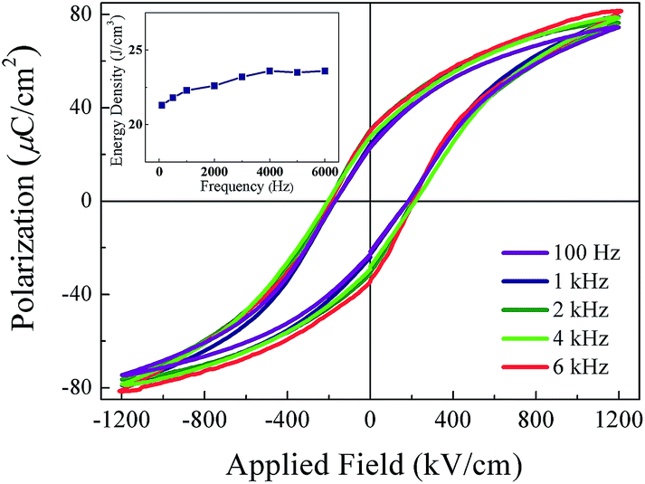
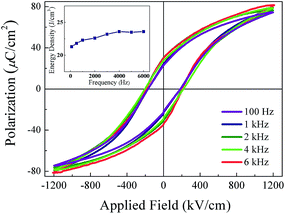
The polarization-applied field hysteresis loops of the 860 nm-thickness NKBT-Sc-c film measured at a frequency range from 100 Hz to 6 kHz is shown in Fig. 9. It is observed that both the Pmax and Pr values slightly decrease with an increase of measurement frequency. According to these results, the inset depicts the frequency dependent energy density of the 860 nm-thickness NKBT-Sc-c film. Because of the small variation of the Pmax − Pr values, the energy storage density W slightly changes in a small range of about 21.6 J cm−3 and 23.2 J cm−3 in the measurement frequency range, indicating a good frequency dependent stability.
 |
| | Fig. 9 Applied field dependent hysteresis loops of the three kinds of 860 nm-thickness NKBT-Sc-c film measured at a frequency range of 100 Hz to 6 kHz. The inset shows frequency-dependent energy density of the 860 nm-thickness NKBT-Sc-c film. | |
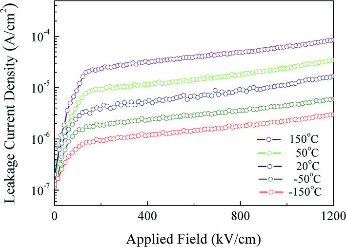
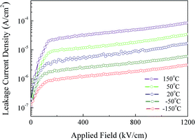
Low leakage current density is always essential for the application of ferroelectric materials in high performance storage devices. The applied field dependence with the leakage current density (J) of the 860 nm-thickness NKBT-Sc-c film was measured at a temperature range from −150 °C to 150 °C, and the results are shown in Fig. 10. It was observed that the J value increased slightly as the measurement temperature increased from −150 °C to 150 °C, and did not break down under 1200 kV cm−1 at 150 °C. Furthermore, the J value maintained a relatively low value throughout the measurement temperature range, which indicated that the NKBT-Sc-c film can work over a wide operating temperature. This low leakage current density can mainly be attributed to a reduction of charged defects at the NKBT-Sc film–TiO2 interface and grain boundary density in the films.
 |
| | Fig. 10 Applied field-dependent leakage current density J of the 860 nm-thickness NKBT-Sc-c film measured at a temperature range from −150 to 150 °C. | |
4. Conclusion
The (100)-oriented NKBT-Sc films with thicknesses ranging from about 460 to 860 nm were fabricated by an aqueous sol–gel method on a platinized silicon substrate through alternately introducing TiO2 layers. Additionally, effects of TiO2 seeds on microstructure and electrical properties were investigated over a temperature range from −150 °C to 150 °C and a frequency range from 100 Hz to 6 kHz. The TiO2 layer coated inside the films can greatly enhance the (100) texture degree, which did not decrease as the thickness increased, and moreover are beneficial for the crystallization process of the NKBT-Sc films. Compared with the NKBT-Sc films without TiO2 seeds, the TiO2-coated NKBT-Sc films exhibit a great enhancement in electric properties as well as energy storage performance. Consequently, a high dielectric constant of about 782 and a low dielectric loss of about 0.051 at 1 kHz, together with an enhanced energy density of about 22.7 J cm−3 and efficiency of about 51.5%, were achieved in the 860 nm-thickness NKBT-Sc-c film at room temperature. Besides, the TiO2-coated NKBT-Sc films exhibit a greatly enhanced temperature dependent energy storage stability in a temperature range from −150 °C to 150 °C, together with a frequency dependent energy storage stability in the frequency range from 100 Hz to 6 kHz. This great enhancement in the dielectric response and energy storage performance can be attributed to higher domain walls motion by increasing crystallinity and (100)-preferred orientation in the films. In addition, the J value of the 860 nm-thickness NKBT-Sc-c film maintains a relatively low value throughout the measurement temperature range, which also means that it can work in a wide operating temperature range.
Conflicts of interest
There are no conflicts to declare.
Acknowledgements
The work was supported by the National Natural Science Foundation of China (Grant No. 51402020), the Natural Science Foundation of Hubei Province of China (Grant No. 2017CFB526), and the Educational Commission of Hubei Province of China (Grant No. D20172803).
References
- K. Wasa, T. Matsushima and H. Adachi, Thin-film piezoelectric materials for a better energy harvesting MEMS, J. Microelectromech. Syst., 2012, 21, 451–457 CrossRef CAS.
- D. L. Polla and L. F. Francis, Ferroelectric thin films in micro-electromechanical systems applications, MRS Bull., 1996, 21, 59–65 CrossRef CAS.
- S. K. Dey and R. Zuleeg, Integrated sol-gel PZT thin-films on Pt, Si, and GaAs for non-volatile memory applications, Ferroelectrics, 1990, 108, 37–46 CrossRef CAS.
- S. Teranishi, M. Suzuki, Y. Noguchi, M. Miyayama, C. Moriyoshi, Y. Kuroiwa, K. Tawa and S. Mori, Giant strain in lead-free (Bi0.5Na0.5)TiO3-based single crystals, Appl. Phys. Lett., 2008, 92, 1829051–1829053 CrossRef.
- M. Abazari, A. Safari, S. S. N. Bharadwaja and S. Trolier-McKinstry, Dielectric and piezoelectric properties of lead-free (Bi,Na)TiO3-based thin films, Appl. Phys. Lett., 2010, 96, 082903 CrossRef.
- X. J. Zheng, J. Y. Liu, J. F. Peng, X. Liu, Y. Q. Gong, K. S. Zhou and D. H. Huang, Effect of potassium content on electrostrictive properties of Na0.5Bi0.5TiO3-based relaxor ferroelectric thin films with morphotropic phase boundary, Thin Solid Films, 2013, 548, 118–124 CrossRef CAS.
- F. Gao, X. Dong, C. Mao, W. Liu, H. Zhang, L. Yang, F. Cao, G. Wang and J. Jones, Energy-storage properties of 0.89Bi0.5Na0.5TiO3-0.06BaTiO3-0.05K0.5Na0.5NbO3 lead-free anti-ferroelectric ceramics, J. Am. Ceram. Soc., 2011, 94, 4382–4386 CrossRef CAS.
- K. Sakata, T. Takenaka and Y. Naitou, Phase relations, dielectric and piezoelectric properties of ceramics in the system (Bi0.5Na0.5)TiO3-PbTiO3, Ferroelectrics, 1992, 131, 219–226 CrossRef CAS.
- O. Elkechai, P. Marchet, P. Thomas and M. Manier, Jean-Pierre Mercurio, Structural and dielectric study of the Na0.5Bi0.5TiO3-PbTiO3 and K0.5Bi0.5TiO3-PbTiO3 systems, J. Mater. Chem., 1997, 7, 91–97 RSC.
- P. Lia, J. W. Zhai, B. Shen, W. Li, H. R. Zeng and K. Y. Zhao, High recoverable energy storage density and large piezoelectric response in (Bi0.5Na0.5)TiO3-PbTiO3 thin films prepared by a sol-gel method, J. Eur. Ceram. Soc., 2017, 37, 3319–3327 CrossRef.
- Z. Xu, X. Hao and S. An, Dielectric properties and energy-storage performance of (Na0.5Bi0.5)TiO3-SrTiO3 thick films derived from polyvinylpyrrolidone-modified chemical solution, J. Alloys Compd., 2015, 639, 387–392 CrossRef CAS.
- V. K. Prateek and R. K. Thakur, Gupta, Recent progress on ferroelectric polymer-based nanocomposites for high energy density capacitors: synthesis, dielectric properties, and future aspects, Chem. Rev., 2016, 116, 4260–4317 CrossRef CAS PubMed.
- Q. G. Chi, J. F. Dong, C. H. Zhang, C. P. Wong, X. Wang and Q. Q. Lei, Nano iron oxide-deposited calcium copper titanate/polyimide hybrid films induced by an external magnetic field: toward a high dielectric constant and suppressed loss, J. Mater. Chem. C, 2016, 4, 8179–8188 RSC.
- Q. G. Chi, T. Ma, Y. Zhang, Y. Cui, C. H. Zhang, J. Q. Lin, X. Wang and Q. Q. Lei, Significantly enhanced energy storage density for poly(vinylidenefluoride) composites by induced PDA-coated 0.5Ba(Zr0.2Ti0.8)O3-0.5(Ba0.7Ca0.3)TiO3 nanofibers, J. Mater. Chem. A, 2017, 5, 16757–16766 CAS.
- Q. G. Chi, T. Ma, J. F. Dong, Y. Cui, Y. Zhang, C. H. Zhang, S. C. Xu, X. Wang and Q. Q. Lei, Enhanced thermal conductivity and dielectric properties of iron oxide/polyethylene nanocomposites induced by a magnetic field, Sci. Rep., 2017, 7, 3072–3082 CrossRef PubMed.
- T. Yu, K. W. Kwok and H. L. W. Chan, The synthesis of lead-free ferroelectric Bi0.5Na0.5TiO3-Bi0.5K0.5TiO3 thin films by sol-gel method, Mater. Lett., 2007, 61, 2117–2120 CrossRef CAS.
- Y. Y. Wu, X. H. Wang, C. F. Zhong and L. T. Li, Effect of Na/K excess on the electrical properties of Na0.5Bi0.5TiO3-K0.5Bi0.5TiO3 thin films prepared by sol-gel processing, Thin Solid Films, 2011, 519, 4798–4803 CrossRef CAS.
- Y. Y. Wu, X. H. Wang, C. F. Zhong and L. T. Li, Effect of anneal conditions on electrical properties of Mn-Doped (Na0.85K0.15)0.5Bi0.5TiO3 thin films prepared by sol-gel method, J. Am. Ceram. Soc., 2011, 94, 1843–1849 CrossRef CAS.
- S. T. Zhang, B. Yang and W. Cao, The temperature-dependent electrical properties of Bi0.5Na0.5TiO3-BaTiO3-Bi0.5K0.5TiO3 near the morphotropic phase boundary, Acta Mater., 2012, 60, 469–475 CrossRef CAS.
- W. Li, H. Zeng, J. Hao and J. Zhai, Enhanced dielectric and piezoelectric properties of Mn doped (Bi0.5Na0.5)TiO3-(Bi0.5K0.5)TiO3-SrTiO3 thin films, J. Alloys Compd., 2013, 580, 157–161 CrossRef CAS.
- W. H. Cui, X. H. Wang and L. T. Li, Large piezoresponse of Na0.5Bi0.5TiO3-K0.5Bi0.5TiO3 thin films prepared via water-based sol-gel method, Ceram. Int., 2015, 41, S37–S40 CrossRef CAS.
- Y. H. Jeon, E. A. Patterson, D. P. Cann, P. Mardilovich, W. Stickel, B. J. Gibbons and S. Zhang, Large piezo response and ferroelectric properties of (Bi0.5Na0.5)TiO3-(Bi0.5K0.5)TiO3-Bi(Mg0.5Ti0.5)O3 thin films prepared by chemical solution deposition, J. Am. Ceram. Soc., 2013, 96, 2172–2178 CrossRef CAS.
- Y. Y. Wu, X. H. Wang and L. T. Li, Effect of Sc-doping on structure and electrical properties of (Na0.85K0.15)0.5Bi0.5TiO3 thin films prepared by sol-gel processing, J. Am. Ceram. Soc., 2011, 94, 2518–2522 CrossRef CAS.
- Z. K. Xie, Z. X. Yue, B. Peng, J. Zhang, C. Zhao, X. H. Zhang, G. Rueh and L. T. Li, Large enhancement of the recoverable energy storage density and piezoelectric response in relaxor-ferroelectric capacitors by utilizing the seeding layers engineering, Appl. Phys. Lett., 2015, 106, 202901 CrossRef.
- Q. G. Chi, J. F. Dong, C. H. Zhang, Y. Chen, X. Wang and Q. Q. Lei, A simple, low-temperature fabrication method of highly (100)-oriented (Na0.85K0.15)0.5Bi0.5TiO3 thin films with outstanding electric properties, J. Alloys Compd., 2017, 704, 336–342 CrossRef CAS.
- J. Li, J. Yu, G. Peng, Y. B. Wang and W. L. Zhou, The influence of the thickness of TiO2 seeding layer on structural and electrical properties of Bi3.15Nd0.85Ti3O12 thin films, J. Phys. D: Appl. Phys., 2007, 40, 3788–3792 CrossRef CAS.
- K. Aoki, Y. Fukuda and K. Numata, Effects of titanium buffer layer on lead-zirconate-titanate crystallization processes in sol-gel deposition technique, Jpn. J. Appl. Phys., Part 1, 1995, 34, 192–195 CAS.
- Z. G. Li, Y. X. Wu and S. Miyake, Metallic sputtering growth of high quality anatase phase TiO2 films by inductively coupled plasma assisted DC reactive magnetron sputtering, Surf. Coat. Technol., 2009, 203, 3661–3668 CrossRef CAS.
- K. Karthik, S. K. Pandian and N. V. Jaya, Effect of nickel doping on structural, optical and electrical properties of TiO2 nanoparticles by sol-gel method, Appl. Surf. Sci., 2010, 256, 6829–6833 CrossRef CAS.
- A. Sasaki, T. Chiba, Y. Mamiya and E. Otsuki, Dielectric and Piezoelectric Properties of (Bi0.5Na0.5)TiO3-(Bi0.5K0.5)TiO3 Systems, Jpn. J. Appl. Phys., Part 1, 1999, 38, 5564–5567 CrossRef CAS.
- C. R. Cho, W. J. Lee, B. G. Yu and B. W. Kim, Dielectric and ferroelectric response as a function of annealing temperature and film thickness of sol-gel deposited Pb(Zr0.52Ti0.48)O3 thin film, J. Appl. Phys., 1999, 86, 2700 CrossRef CAS.
- D.
V. Taylor and D. Damjanovic, Evidence of domain wall contribution to the dielectric permittivity in PZT thin films at sub-switching fields, J. Appl. Phys., 1997, 82, 1973 CrossRef CAS.
- B. J. Chu, X. Zhou, K. L. Ren, B. Neese, M. R. Lin, Q. Wang, F. Bauer and Q. M. Zhang, A dielectric polymer with high electric energy density and fast discharge speed, Science, 2006, 313, 334–336 CrossRef CAS PubMed.
- Z. Xie, B. Peng, S. Meng, Y. Zhou, Z. Yue and S. E. Trolier-McKinstry, High-energy-storage density capacitors of Bi(Ni1/2Ti1/2)O3-PbTiO3 thin films with good temperature stability, J. Am. Ceram. Soc., 2013, 96, 2061–2064 CrossRef CAS.
- G. Viola, H. Ning, M. J. Reece, R. Wilson, T. M. Correia, P. Weaver, M. G. Cain and H. Yan, Reversibility in electric field-induced transitions and energy storage properties of bismuth-based perovskite ceramics, J. Phys. D: Appl. Phys., 2012, 45, 355302 CrossRef.
- L. H. Luo, B. Y. Wang, X. X. Jiang and W. P. Li, Energy storage properties of (1-x)(Bi0.5Na0.5)TiO3-xKNbO3 lead-free ceramics, J. Mater. Sci., 2014, 49, 1659–1665 CrossRef CAS.
- F. Gao, X. L. Dong, C. L. Mao, F. Cao and G. S. Wang, c/a ratio-dependent energy-storage density in (0.9-x)Bi0.5Na0.5TiO3-xBaTiO3-0.1K0.5Na0.5NbO3 ceramics, J. Am. Ceram. Soc., 2011, 94, 4162–4164 CrossRef CAS.
Footnote |
| † These authors contributed equally to this work. |
|
| This journal is © The Royal Society of Chemistry 2017 |
Click here to see how this site uses Cookies. View our privacy policy here. 
 Open Access Article
 This Open Access Article is licensed under a Creative Commons Attribution-Non Commercial 3.0 Unported Licence
 *a,
Yonghong Hu†b,
Xiaohui Wangc,
Caifu Zhongd and
Longtu Lic
*a,
Yonghong Hu†b,
Xiaohui Wangc,
Caifu Zhongd and
Longtu Lic
 of 56 pm V−1) properties in polycrystalline 0.85(Na0.5Bi0.5)TiO3–0.15(K0.5Bi0.5)TiO3 (NKBT) thin films.17 Moreover, it was reported that substitution of an A-site can obtain a relatively higher saturated polarization and/or lower remnant polarization, both of which are beneficial for improving its energy-storage density. Jeon et al. prepared a Mg-doped NBT-KBT thin film with ferroelectric (Pr = 12 μC cm−2, Pmax = 52 μC cm−2) and piezoelectric (
 ) properties by chemical solution deposition.22 According to our research, with an appropriate concentration Sc substitution in a NKBT film, a ferroelectric property (Pr = 18.6 μC cm−2, Pmax = 57.4 μC cm−2) and piezoelectric property (
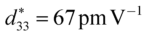 ) were obtained.23
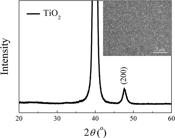


 ), energy loss Wloss and energy efficiency η (η = W/(W + Wloss)) in dielectric capacitors can be calculated from the P–E loops.33,34 Ferroelectric materials with higher dielectric breakdown strength (BDS) and larger differences between Pmax and Pr have the potential to be applied in electronic devices and systems such as high energy-storage capacitors. Fig. 7(c) depicts the applied field dependent energy density and efficiency of these three kinds of NKBT-Sc films. According to the calculated results, the energy density W and energy efficiency η of these three kinds of films, with thicknesses of about 460 nm and 860 nm at 1200 kV cm−1, are listed in Table 2. The P–E loops of the 860 nm-thickness NKBT-Sc-c film measured at room temperature under different electric fields are shown in Fig. 7(d). The energy storage density W of these three kinds of NKBT-Sc films are found to increase almost linearly with increasing applied field, while in the meantime the energy efficiency η shows an opposite tendency. The TiO2 layer has a strong impact on energy-storage performance and moreover this performance greatly enlarges by deliberately engineering a strong TiO2 layer. The 860 nm-thickness NKBT-Sc-c film exhibits the best energy-storage performance among the three kinds of NKBT films with a W value of about 22.7 J cm−3 and an efficiency η of about 51.5%, while the 860 nm-thickness NKBT-Sc-a film showed a W value of about 12.3 J cm−3 and η value of about 43.7% at 1200 kV cm−1. In addition, the thicker TiO2-coated NKBT-Sc films (860 nm-thickness) exhibit a higher W value together with a lower η value than the 460 nm-thickness ones. Energy density obtained at a low applied field in the TiO2-coated NKBT-Sc films in this work is superior to the values reported for NBT-based ceramics.35–37