
 Open Access Article
 This Open Access Article is licensed under a
 Creative Commons Attribution 3.0 Unported Licence
Quasiparticle energies, exciton level structures and optical absorption spectra of ultra-narrow ZSiCNRs†
Ping Lou
Department of Physics, Anhui University, Hefei 230039, Anhui, China. E-mail: loup@ahu.edu.cn; Fax: +86-551-65107999; Tel: +86-551-65106477
First published on 9th November 2017
Abstract
The hydrogen-passivated N chain zigzag silicon carbide nanoribbons (N-ZSiCNRs) are indexed by their width N (the number of zigzag Si–C chains across the nanoribbon). Based on first-principles GW and Bethe–Salpeter equation (BSE) approaches, we investigated the quasiparticle band structures, exciton level structures and optical absorption spectra of the ultra-narrow N-ZSiCNRs with N = 2–3. It is found that the GW band gap of 3-ZSiCNR is 0.804 eV, which is more than two times larger than the HSE06 band gap (0.401 eV). The GW band gap of 2-ZSiCNR is 2.911 eV, which is also almost more than two times larger than the HSE06 band gap (1.621 eV). These results indicate that for 1-dimensional structure materials, HSE06 approaches underestimate the band gap of the system. The GW + BSE calculations demonstrate that the optical absorption spectra of the N-ZSiCNRs are dominated by edge-state-derived excitons with large binding energy, composed of a characteristic series of exciton states. It is found that the edge-state excitons of N-ZSiCNR belong to charge-transfer excitons, where the excited electron is confined to a Si edge while the hole is located on a C edge. The exciton binding energy increases with decreasing width N, which indicates that the quantum confinement effect enhances with decreasing width N. The excitons in 2-ZSiCNR can have a binding energy up to 1.78 eV. In addition, the exciton level structure and wave function are classified. It is very interesting to find a relationship between the node of the exciton wave functions and the incoming polarization light exciton excitation. For example, in the longitudinal optical absorption spectra, if the exciton whose wave function possesses an odd number of nodes is optically active, then the exciton whose wave function possesses an even number of nodes is optically inactive. In contrast, in the transverse optical absorption spectra, the exciton whose wave function possesses an odd number of nodes is optically inactive, while the exciton whose wave function possesses an even number of nodes is optically active.
1 Introduction
It is known that double edge hydrogenation armchair edge graphene nanoribbons (ARGNRs) belong to nonmagnetic semiconductors; but double edge hydrogenation zigzag edge graphene nanoribbons (ZGNRs) belong to antiferromagnetic (AF) semiconductors, where each zigzag edge exists in the ferromagnetic (FM) order, while the magnetic moments at opposite edge carbon atoms exist as AF coupling.1–4 Son et al. studied the transverse electric field effect on ZGNRs.5 Kim et al.6 studied the spin valve of ZGNRs. It is found that in non-straight edges of graphene nanoribbons, the edge magnetic coupling can be FM coupling.7–9 Yu et al. found a unified geometric rule for designing the magnetic nanostructures of graphene-based nanoribbons.8 In addition, studies reveal that ZGNRs made by functionalization of edges, such as by functional groups or by various atoms, can show various electronic and magnetic properties.10–14 Recently, Chen et al. studied the room-temperature spin caloritronics effect of sawtooth ZGNRs.15 Krepel et al. demonstrated that AGNRs can be used as ultrasensitive chemical detectors.16Unlike graphene,17 which is a zero-band-gap semiconductor, SiC sheet, a new SiC lower dimensional structure material, is a wide-band-gap semiconductor.18–20 SiC sheet nanoribbons (SiCNRs) are shown in Fig. 1(a) and 2(a), where the edge silicon and carbon atoms are referred to as edge Si and edge C atoms, whereas the corresponding edges are called Si-edge and C-edge, respectively. Spin-polarized first-principles calculations show that armchair SiCNRs (ASiCNRs) are nonmagnetic semiconductors,18,19 while N chain zigzag SiCNRs (N-ZSiCNRs) are magnetic metals.18 A further study by Lou and Lee revealed that the N-ZSiCNRs (3 ≤ N ≤ 6) are ferrimagnetic semiconductors of which the spin-up and spin-down channels have different direct band gaps, but 2-ZSiCNR has only a nonmagnetic semiconducting state with a direct band gap.21 Moreover, they found that by applying an external transverse electric field22 or carrier (hole and electron) doping,23,24 the N-ZSiCNRs can be utilized for manipulating the magnetization. Recently, Zheng et al.25 found that the band-gap of SiCNRs can be modulated by transverse electric fields. In addition, the edge reconstruction effect,26 edge hydrogenation,28 NM impurity chemistry substitution,27,29 Stone–Wales defects,30 edge-modification,31,32 as well as molecular surface-adsorbing33,34 on the electrical and magnetic properties of N-ZSiCNRs have also been investigated. Recently, Wu et al. studied the spin caloritronics effect of the N-ZSiCNR heterostructure.35
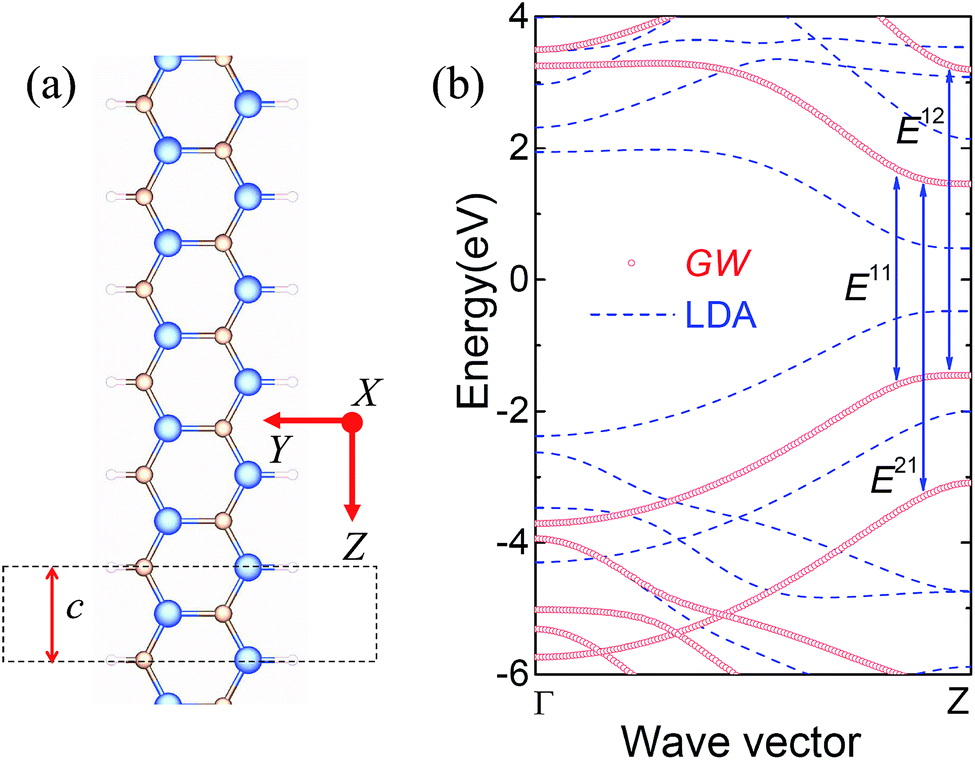 | ||
| Fig. 1 (a) Geometry structure of 2-ZSiCNR. The dark yellow, blue and white balls represent C atoms, Si atoms and H atoms, respectively. The system is periodic along the Z-direction. c is the lattice constant (3.116 Å) along the periodic direction. (b) Electronic band structures in the first Brillouin zone along the ribbon. The red open circles indicate the GW band structures while the blue dashed lines indicate the LDA band structures. The Fermi level is set to zero. The vertical blue arrows represent the interband transitions. Eij denotes the interband transition energy from the ith valence band to the jth conduction band, with the band indices counted from the Fermi level. | ||
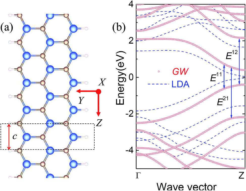 | ||
| Fig. 2 (a) Geometry structure of 3-ZSiCNR. The dark yellow, blue and white balls represent C atoms, Si atoms and H atoms, respectively. The system is periodic along the Z-direction. c is the lattice constant (3.116 Å) along the periodic direction. (b) Electronic band structures in the first Brillouin zone along the ribbon. The red open circles indicate the GW band structures while the blue dashed lines indicate the LDA band structures. The Fermi level is set to zero. The vertical blue arrows denote the interband transitions. Eij denotes the interband transition energy from the ith valence band to the jth conduction band, with the band indices counted from the Fermi level. | ||
More recently, the electronic and magnetic properties of N-ZSiCNRs have been investigated using the Heyd–Scuseria–Ernzerhof screened hybrid functional (HSE06) with a plane-wave basis set,36 which confirm that 2-ZSiCNR and 3-ZSiCNR are new direct band gap semiconductors. The HSE06 band gap is 1.517 eV and 0.401 eV for the 2-ZSiCNR and 3-ZSiCNR,36 respectively, which may be quite interesting from the perspective of photochemical catalysis and solar cells. Thus, it is highly required to understand the excited-state properties of N-ZSiCNRs. However, so far research is focused on the ground state properties of N-ZSiCNRs. The fundamental excited-state properties of N-ZSiCNRs, such as quasiparticle (QP) band structures, exciton structures and optical absorption spectra, have not been paid enough attention, although recently Alaal et al. studied the QP band structure and optical absorption spectrum of N-ZSiCNRs. Moreover, Alaal et al. revealed that the GW band gap of 2-ZSiCNR was 2.4 eV,37 which is larger than the HSE06 band gap (1.517 eV).36 However, they found that the GW band gap of 3-ZSiCNR was 0.45 eV,37 which is almost equal to the HSE06 band gap (0.401 eV).36
On the other hand, it is known that in low dimensional structure materials, such as graphene, carbon nanotubes, GNRs, as well as SiC sheets and single-walled SiC nanotubes, the electron–electron (e–e) correlations and electron–hole (e–h) interactions play a very important role in the electronic band structure and optical properties.38–48 This is due to the fact that there are two key effects in low dimensional structure materials: one is the quantum confinement effect, another is the less efficient electronic screening effect. These two key effects will not only give rise to the enhancement of the electron–electron (e–e) correlations, where the enhanced electron–electron (e–e) correlations will lead to a large QP energy gap, but also the quantum confinement effect leads to a large overlap between the electron and hole wave functions resulting in reduced screening between e–h excitations, as a result, this leads to the formation of strongly bound excitons. Since ultra-narrow N-ZSiCNRs are a one-dimensional structure semiconductor, one can expect that there is a strong exciton effect in such a system. However, Alaal et al. show that 2-ZSiCNR has only one strongly bound exciton, originating from optical transition between the first valence band and the first conduction band around the Brillouin zone (BZ) Z-point.37 What is even more surprising is that unlike 2-ZSiCNR, 3-ZSiCNR does not have any strongly bound excitons.37 Why? Is that really so? To answer these questions, it is naturally needed to further study the quasiparticle band structures and optical absorption spectra of the 2-ZSiCNRs and 3-ZSiCNRs.
Motivated by the above issues, we perform first-principles GW49,50 and Bethe–Salpeter equation (BSE)50,51 approaches to study the QP band structures, exciton level structures and optical absorption spectra of the 2-ZSiCNRs and 3-ZSiCNRs. It is excitingly found that the GW band gap of 3-ZSiCNR is 0.804 eV, which is almost more than two times larger than the Alaal et al.37 GW band gap (0.45 eV). The GW band gap of 2-ZSiCNR is 2.911 eV, which is also larger than the Alaal et al.37 GW band gap (2.4 eV). Moreover, it is found that the optical absorption spectra of the 2-ZSiCNRs are dominated by edge-state-derived excitons with large binding energy, composed of a characteristic series of exciton states, instead of only one exciton state. Even more excitingly, just like 2-ZSiCNR, the optical absorption spectra of the 3-ZSiCNRs are also dominated by edge-state-derived excitons with large binding energy, composed of a characteristic series of exciton states. The edge-state excitons of N-ZSiCNR belong to charge-transfer excitons, where the excited electron is confined to the Si edge, while the hole is confined to the C edge. The exciton binding energy increases with decreasing width N, which indicates that the quantum confinement effect enhances with decreasing width N. The excitons in 2-ZSiCNR can have a binding energy up to 1.78 eV. In addition, the exciton level structure and wave function characteristics are classified. It is very interesting to find a relationship between the node of the exciton wave functions and the incoming polarization light exciton excitation; for example when the incoming polarization light is parallel to the ribbon axis, the exciton whose wave function possesses an odd number of nodes is optically active, while the exciton whose wave function possesses an even number of nodes is optically inactive. However, when changing the light polarization from parallel to perpendicular to the ribbon axis, the exciton whose wave function possesses an odd number of nodes will become optically inactive, while the exciton whose wave function possesses an even number of nodes will become optically active. Lastly, the results that Alaal et al. recently studied are discussed.
2 Computational methods and model system
2.1 Model system
Regarding the model system, as shown in Fig. 1(a) and 2(a), we adopted a super cell geometry where the length of a vacuum region along the non-periodic direction (X- and Y-directions) was 28 Å. The lattice constant (c) along the periodic direction (Z-direction) was 3.116 Å,36 which is in agreement with the findings of other researchers.18,37 A zigzag silicon carbon nanoribbon that is hydrogen-terminated (N-ZSiCNR) can be indexed by a width N, where N is the number of parallel zigzag chains across the ribbon width, such as that shown in Fig. 1(a) for N = 2 and shown in Fig. 2(a) for N = 3.2.2 Electronic ground state
Standard density functional theory (DFT) with a local density approximation (LDA) functional (DFT-LDA) is used for treating all the electronic ground states of the systems, and is performed using the Quantum-ESPRESSO package.52 The plane-wave cutoff was set as 60 Ry with a norm-conserving pseudopotential. The BZ integration has been performed with 1 × 1 × 64 k-point sampling points in the calculations. The structures were fully relaxed until an energy convergence of 10−9 Ry and a force convergence on atoms of 0.01 eV Å−1 were reached.2.3 GW approximation
From the DFT-LDA wave functions and corresponding eigenvalues calculated above, the many-body effects on the QP band structure are calculated within the GW approximation, which is performed using the BerkeleyGW package.50 In detail, starting from the DFT-LDA wave functions and Coulomb screening, the QP energies (Enk) are obtained by solving the Dyson’s equation:49,50| [H0 + ∑(Enk)]ψnk = Enkψnk | (1) |
2.4 Excitonic effects and exciton
The excitonic effects (electron–hole interactions), which are not included in GW itself, are included by solving the BSE in terms of two-particle Green’s function, which is also performed using the BerkeleyGW package.50 In detail, in the quasi-electron state |ck〉 and quasi-hole state |vk〉 direct product space |vck〉 (|vck〉 = |vk〉|ck〉), the electron–hole excited state (|S〉) is represented by the expansion50,51
 | (2) |
The amplitude AvckS is the excitonic wave function of the Sth exciton in k-space, which is obtained by solving the BSE50,51
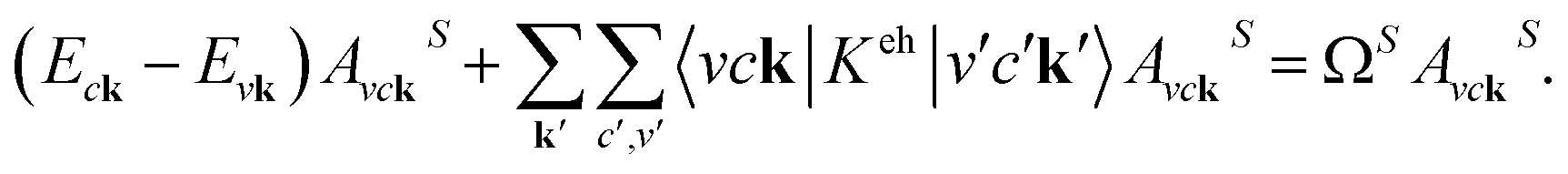 | (3) |
The eigenvalue Ωs is the excitonic energy of the Sth exciton. Evk and Eck indicate quasiparticle energies for the valence band state |vk〉 and conduction band state |ck〉 at a specific k point, respectively. Keh is the kernel, which describes the interaction between excited electrons and holes. For calculating, the kernel Keh of the N-SiCNRs is computed on a coarse k-point grid of 1 × 1 × 64 and then interpolated onto a fine k-point grid of 1 × 1 × 256 to get converged exciton states,50,51 and the Coulomb truncation scheme has been adopted.39,44,45
On the other hand, in re and rh coordinate representation, ϕck(re) = 〈re|ck〉, ϕvk(rh) = 〈rh|vk〉, and ΦS(re,rh) = 〈re,rh|S〉, and then by eqn (2), the excitonic wave function in real space can be expressed as50,51
 | (4) |
2.5 Exciton energy level and binding energy
By solving eqn (3) we can get the exciton energy ΩS, i.e., the excitonic energy of the S exciton. It is noted that S is an index mark in all excitons. In order to more clearly describe which quasi-electron and quasi-hole interaction leads to ΩS, we define the exciton energy level Enij, i.e., the excitonic energy of the nth exciton that the ith quasi-hole and jth quasi-electron interactions result in.The exciton binding energy Ebij(n) is defined as
| Ebij(n) = Eij − Enij, | (5) |
2.6 Excitation optical absorption spectra
It is known that the excitation optical absorption spectra, one of the most fundamental techniques for directly probing electronic transitions in materials, are determined by the imaginary part of the macroscopic dielectric function ε2(ω), which can be expressed as:50,51
 | (6) |
In contrast, when Keh = 0, ΩS = Eck − Evk, and then eqn (6) is reduced to
 | (7) |
Such a result ignores the e–h interactions, marked as “without e–h” in the following.
It should be mentioned that the optical absorption spectra have a relationship with the incoming light polarization direction e. In this paper, we research two different kinds of incoming light polarization direction e, namely, (a) the e that is parallel to the Z-axis, i.e., along the N-ZSiCNR axis, called the longitudinal optical absorption spectrum and (b) the e that is perpendicular to the Z-axis and is parallel to the Y-axis, called the transverse absorption spectrum. Of course, compared with the longitudinal optical absorption spectrum, the transverse absorption spectrum should be strongly suppressed owing to the ribbon geometrical anisotropy and the depolarization effect it produces.53
More details concerning the GW and BSE methods can be found in ref. 49–51.
3 Results and discussion
3.1 QP band structure
The GW and LDA band structures of 2-ZSiCNR and 3-ZSiCNR in the ground state are shown in Fig. 1(b) and 2(b), respectively. The blue dashed lines display the LDA band structures exhibiting a direct band gap at the Z point (0.957 eV for 2-ZSiCNR and 0.093 eV for 2-ZSiCNR), which is in good agreement with the recent PBE results.21 The red open circles show the GW band structures. It is clear that when the e–e self-energy effects are included using the GW approximation, the band structure is strongly modified, except the direct band gap located at the Z point. As shown in Fig. 1(b) in the red open circles, the GW band gap of 2-ZSiCNR is 2.911 eV, which is more than three times larger than the LDA band gap (0.927 eV) and is also larger than a recent GW band gap (2.4 eV).37 As shown in Fig. 2(b) in the red open circles, the GW band gap of 3-ZSiCNR is 0.804 eV, which is more than 9 times larger than the LDA band gap (0.093 eV) and is also almost more than two times larger than the recent GW band gap (0.45 eV).37 Such large GW QP corrections to the LDA band gap originate from the enhance of e–e interactions owing to the enhanced quantum confinement and less efficient electronic screening in 1-dimensional structure semiconducting materials. Clearly, such nonlocal behavior can not be correctly described by the LDA.It is noted that the HSE06 functional has considered nonlocal exchange effects. However, the HSE06 functional results in a remarkably smaller gap than the GW gap, as is listed in Table 1, and the use of the HSE06 functional decreases the GW band gap from 2.911 eV to 1.621 eV for the 2-ZSiCNR, as well as from 0.804 eV to 0.401 eV for the 3-ZSiCNR. Therefore, the coulomb screening effect, which is only well described by the self-energy operator in the GW method, plays a significant role in the electronic structure of N-SiCNR.
| N-SiCNR | LDA | HSE06 | GW |
|---|---|---|---|
| N = 2 | 0.957 | 1.621 | 2.911 |
| N = 3 | 0.093 | 0.401 | 0.804 |
Moreover, as is listed in Table 1, the GW band gap of 3-ZSiCNR is 0.804 eV, which is not only more than nine times larger than the LDA band gap (0.093 eV), but also more than two times larger than the HSE06 band gap (0.401 eV). The GW band gap of 2-ZSiCNR is 2.911 eV, which is more than three times larger than the LDA band gap (0.957 eV) and is also almost more than two times larger than the HSE06 band gap (1.621 eV), indicating that for 1-dimensional structure materials, not only do LDA approaches underestimate the band gap of the system, but also HSE06 approaches underestimate the band gap of the system.
In addition, GW QP corrections exhibit a complicated energy and momentum dependence. As shown in Fig. 1(b) and 2(b), the downward translation of the valence band and upward translation of the conduction band give rise to the band gap widening. Meanwhile, a renormalization effect results in the slope in the dispersion relation of the bottom conduction bands and top valence bands increasing. This renormalization effect also occurs in other 1-dimensional structure materials, such as single-walled carbon nanotubes and GNRs, as well as single-walled SiCNTs. Such behavior originates from the nonlocal character of the self-energy operator in the GW method. Therefore, one cannot use a simple “scissor rule” to obtain the QP band structure of N-SiCNR.
3.2 Optical absorption spectra
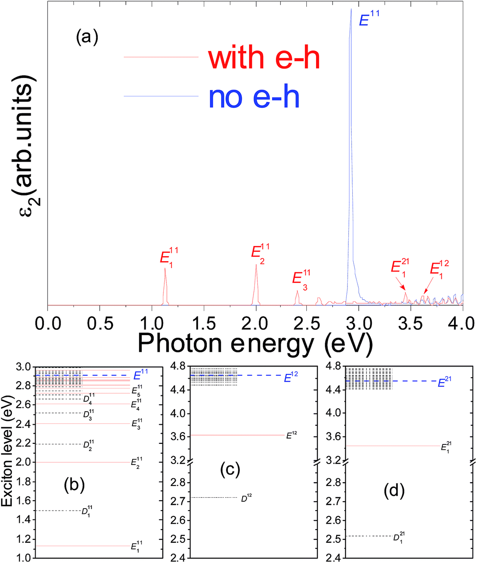
As shown in Fig. 1(b) and 2(b), near the Z-point of the Brillouin zone, the electronic bands of 2-ZSiCNR and 3-ZSiCNR are nearly flat, which of course cannot be approximated by parabolic curves. Moreover, just like in single-walled carbon nanotubes system,42 the coulomb screening in the N-ZSiCNR system highly depends on the electron–hole separation. As a result, the usually hydrogenic-like model of the exciton is no longer appropriate for excitons in N-ZSiCNRs. In the N-ZSiCNR, it is these unusual features that lead to several unique characteristics of its bound exciton spectrum. The longitudinal optical absorption spectra of the 2-SiCNR and 3-SiCNR, with and without electron–hole interaction, are shown in Fig. 3(a) and 5(a), respectively, while the transverse absorption spectra of the 2-SiCNR and 3-SiCNR, with and without electron–hole interaction, are shown in Fig. 4(a) and 6(a), respectively. The optical transitions that give rise to the optical absorption peaks without electron–hole interactions (blue lines in Fig. 3(a), 4(a), 5(a), and 6(a)) are marked with blue arrows on the electronic band structures in Fig. 1(b) and 2(b). The red lines in Fig. 3(a), 4(a), 5(a), and 6(a) indicate the optical absorption spectra including the electron–hole interactions. It should be pointed out that a Gaussian broadening of 0.01 eV is applied to all spectra, which is in agreement with that discussed in the spectra of ARGNRs and ZGNRs.44,45 This is a because larger Gaussian broadening will lead to the fact that two peaks that are close to each other can not be distinguished (refer to ESI Fig. 1 and 2†).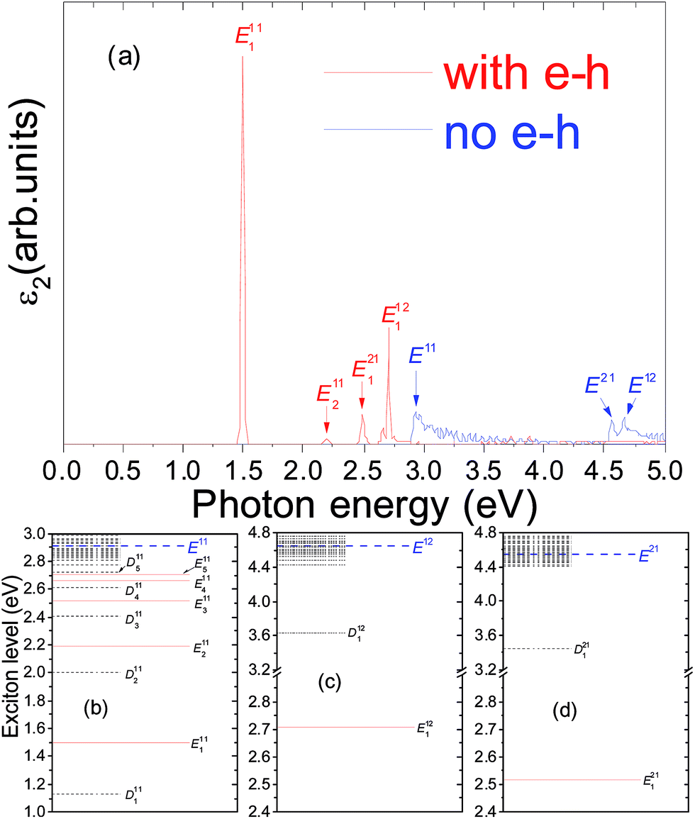 | ||
| Fig. 3 (a) The longitudinal optical absorption spectra of 2-ZSiCNR with (red lines) and without (blue lines) including the effect of the electron–hole (e–h) interaction. (b), (c) and (d) are the schematic drawings of the energy levels of the excitons associated with the interband transitions Eij, where Enij and Dnij denote the nth bright and dark exciton states, respectively. The black dashed lines denote the dark exciton levels. The red solid lines show the bright exciton levels. The blue dashed lines denote the energy levels of the interband transitions. | ||
 | ||
| Fig. 4 (a) The transverse optical absorption spectra of 2-ZSiCNR with (red lines) and without (blue lines) including the effect of the electron–hole (e–h) interaction. (b), (c) and (d) are the schematic drawings of the energy levels of the excitons associated with the interband transitions Eij, where Enij and Dnij denote the nth bright and dark exciton states, respectively. The black dashed lines denote the dark exciton levels. The red solid lines show the bright exciton levels. The blue dashed lines denote the energy levels of the interband transitions. | ||
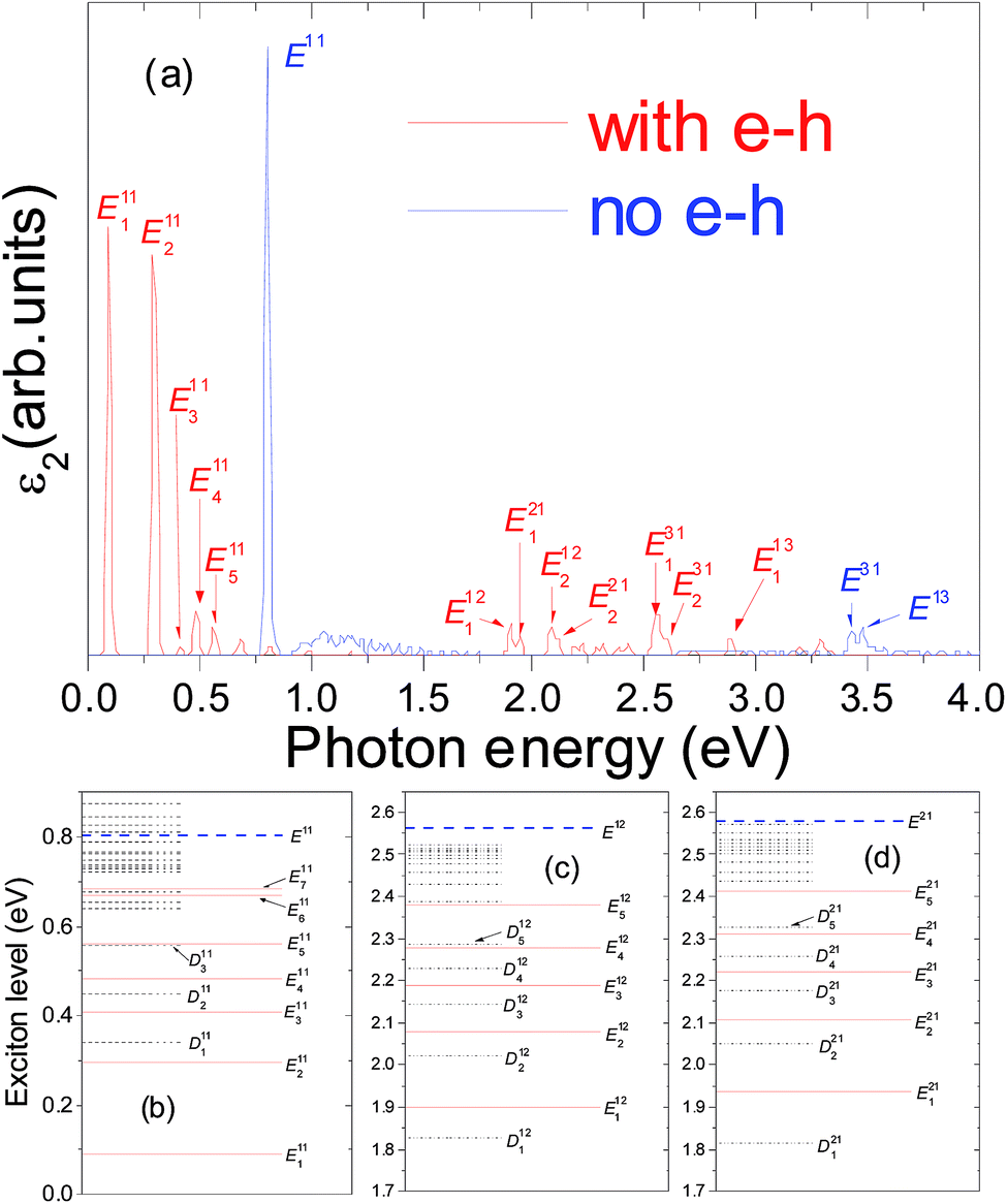 | ||
| Fig. 5 (a) The longitudinal optical absorption spectra of 3-ZSiCNR with (red lines) and without (blue lines) including the effect of the electron–hole (e–h) interaction. (b), (c) and (d) are the schematic drawings of the energy levels of the excitons associated with the interband transitions Eij, where Enij and Dnij denote the nth bright and dark exciton states, respectively. The black dashed lines denote the dark exciton levels. The red solid lines show the bright exciton levels. The blue dashed lines denote the energy levels of the interband transitions. | ||
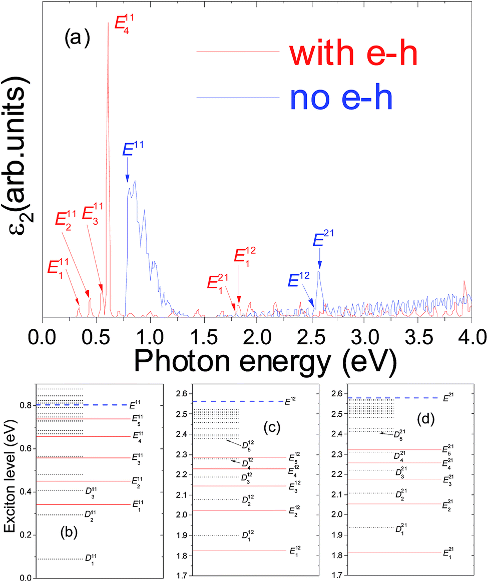 | ||
| Fig. 6 (a) The transverse optical absorption spectra of 3-ZSiCNR with (red lines) and without (blue lines) including the effect of the electron–hole (e–h) interaction. (b), (c) and (d) are the schematic drawings of the energy levels of the excitons associated with the interband transitions Eij, where Enij and Dnij denote the nth bright and dark exciton states, respectively. The black dashed lines denote the dark exciton levels. The red solid lines show the bright exciton levels. The blue dashed lines denote the energy levels of the interband transitions. | ||
It is clear that the quantum confinement effect and less efficient electronic screening in 2-SiCNR and 3-SiCNR not only lead to large GW QP corrections to the LDA band gap, but also result in enhanced excitonic effects with the formation of a bound exciton with considerable binding energy and lead to the entire absorption spectrum changing dramatically, compared with the absorption spectrum without electron–hole interaction. Firstly, inclusion of the electron–hole interaction leads to a significant red shift of the absorption spectrum. Secondly, one of the most striking results of the electron–hole interaction is that new absorption peaks appear below the onset of the continuum interband transition. Clearly, such absorption peaks completely disappear in the absence of electron–hole interaction.
Speaking specifically, for the longitudinal optical absorption spectrum of the 2-SiCNR, in the absence of electron–hole interactions, the interband transitions between the first valence band and the first conduction band around the Z-point give rise to a continuum interband transition peak E11 (see Fig. 3(a)), which is located at 2.911 eV. After including the electron–hole interaction, the entire absorption spectrum of the 2-SiCNR changes dramatically, namely, the continuum interband transition peaks vanish, accompanying the appearance of new peaks below the onset of E11. These dominating new peaks in the absorption spectrum are associated not only with the En11 series of bound excitons but also with the En12 and En21 series of bound excitons, such as E111 and E211 resulting from optical transition between the first valence band and the first conduction band around the Z-point, E112 resulting from optical transition between the first valence band and the second conduction band around the Z-point, and E121 resulting from optical transition between the second valence band and the first conduction band around the Z-point. It is clear that compared with the without electron–hole results, the absorption spectrum including the electron–hole interaction has a red shift with a change in the relative position of the peaks, i.e., the first prominent peak E111 is located at 1.496 eV, which is in the visible light region, whereas the second strongest peak E112 is located at 2.71 eV, which is also in the visible light region. On the other hand, due to the fact that these excitons take off nearly all the continuum transition oscillator strengths, they will possess extraordinarily large electron hole binding energies. As expected, the E111 exciton binding energy Eb11(1) is 1.48 eV. The E112 exciton binding energy Eb12(1) is 1.95 eV. It should be pointed out that E111 is not the lowest energy level of an exciton in the 2-SiCNR. As shown in Fig. 3(b), the lowest energy level of an exciton in the system belongs to D111, which is a dark exciton state. More detailed discussions of the exciton state and level structure are referred to in Section 3.3.
For the longitudinal optical absorption spectrum of the 3-SiCNR, new peaks below the onset of E11 are associated only with the En11 series of bound excitons. However, new peaks associated with the En12 and En21 series of bound excitons (such as E112 and E121) are located above the E11 continuum, which is different compared to the 2-SiCNR. It is noted that the first strongest absorption peak E111 (see Fig. 5(a)) is located at 0.09 eV, which corresponds to an exciton binding energy Eb11(1) of 0.714 eV. Moreover, as shown in Fig. 5(b), E111 is the lowest energy level of an exciton in the 3-SiCNR. Meanwhile the second strongest peak E211, still resulting from optical transition between the first valence band and the second conduction band, is located at 0.29 eV, which corresponds to an exciton binding energy Eb11(2) of 0.514 eV. In addition, the visible light peaks of the 3-SiCNR result from optical transitions between the first valence band and the second conduction band, between the second valence band and the first conduction band, between the first valence band and the third conduction band, and between the third valence band and the first conduction band, such as E112, E121 and E113, as well as E131.
As for the transverse absorption spectra of the 2-SiCNR and 3-SiCNR, compared with the corresponding longitudinal absorption spectra, the absorption peak positions and line shapes change obviously. For example, the lowest-energy absorption peak position of the 2-SiCNR (see Fig. 4(a) red E111) now moves downward to 1.128 eV, which is the position of the D111 dark exciton state in the longitudinal optical absorption spectrum. Now, as shown in Fig. 4(b), E111 is the lowest energy level of an exciton in the 2-SiCNR. The binding energy of the corresponding exciton Eb11(1) is 1.78 eV. Moreover, unlike the longitudinal optical absorption spectrum, where the first prominent peak is E111, we find that the first prominent peak of the transverse absorption spectrum is E211.
For the transverse absorption spectrum of the 3-SiCNR, in contrast to the absorption peak red shift of the 2-SiCNR, the absorption peak of the 3-SiCNR appears to blue shift, i.e., the lowest-energy absorption peak E111 (see Fig. 6(a)) now moves upward to 0.34 eV, which is the position of the D111 dark exciton state in the longitudinal optical absorption spectrum. As a result, as shown in Fig. 6(b), E111 is no longer the lowest energy level of an exciton in the 3-SiCNR. Now, the lowest energy level of an exciton in the system belongs to D111, which is the dark exciton. The binding energy of the corresponding exciton Eb11(1) is 0.464 eV. In addition, unlike the longitudinal optical absorption spectrum, where the first prominent peak is E111, we find that the first prominent peak of the transverse absorption spectrum is E411.
In addition, it should be mentioned that for lower dimensional systems,54,55 the supercell calculation will lead to an artificial size effect on the dielectric function. In order to eliminate such an artificial size effect, for the N-ZSiCNR, the optical spectrum in the polarizability per unit area is defined as α2(ω) = A⊥ε2(ω)/4π, where A⊥ is the cross-sectional area of the supercell perpendicular to the N-ZSiCNR axis. The optical spectra in the polarizability per unit area are shown in ESI Fig. S7 and S8.† Clearly, there is no difference between Fig. 3(a), 4(a), 5(a) and 6(a) and the corresponding Fig. S7(a) and (b) and S8(a) and (b),† except for the unit. This is due to the fact that for a given supercell, A⊥ is a constant.
3.3 Exciton level structure and wave functions
In order to gain further insight into the above results, the exciton level structure and the corresponding exciton wave functions are plotted. The exciton level structure of the 2-ZSiCNR and 3-ZSiCNR are shown in (b), (c) and (d) of Fig. 3, 4, 5, and 6. It should be pointed out that from solving eqn (3) to obtain the excitonic energy, we know that the exciton level structure is the intrinsic property of the system. However, in order to mark whether the excitons are excited in the optical absorption spectrum or not, the excitons are classified into bright excitons (E) and dark excitons (D). In addition, from solving eqn (3) and (6) to obtain the optical absorption spectrum, we know that e·〈0|v|S〉 of eqn (6) represents the Sth exciton contribution to the optical absorption spectrum, namely, e·〈0|v|S〉 will give rise to the Sth exciton peak in the optical absorption spectrum under the e direction polarization light. In general, for the Sth exciton there are two possible results: one is e·〈0|v|S〉 ≠ 0, namely the peak of the Sth exciton will appear in the optical absorption spectrum, which is labelled the bright exciton, i.e., optically active exciton; the other is 〈0|v|S〉 ≠ 0 but e·〈0|v|S〉 = 0, i.e., e⊥〈0|v|S〉, namely, although there exists an Sth exciton, the peak of the Sth exciton does not appear in the optical absorption spectrum, which is labelled the dark exciton, i.e., optically inactive exciton.For example, (b), (c) and (d) of Fig. 3 show the exciton level structure associated with the interband transitions Eij in 2-SiCNR for light polarized along the ribbon axis (e‖Z), where Enij and Dnij denote the nth bright and dark exciton states, respectively. Superscript ij denotes the excitation originated from optical transition between the ith valence band and the jth conduction band, counted from the band gap. In order to describe the exciton level structure more clearly, Enij and Dnij associated with the interband transitions Eij are called as the Eij series of excitons. In the Eij series of excitons, the exciton of the lowest energy level is called the “ground state” exciton. For example, as shown in Fig. 3(b), D111, E111, D211, E211, D311, and E311 belong to the E11 series of excitons. Clearly, D111 is the ground state exciton, which is the dark exciton state. However, when changing the light polarization from parallel (e‖Z) to perpendicular to the ribbon axis (e‖Y), as shown in Fig. 4(b), the ground state exciton turns into E111, i.e., the bright exciton state. For the E12 series of excitons, as shown in Fig. 3(c), the ground state exciton is E112, which is the bright exciton state. However, when changing the light polarization from parallel (e‖Z) to perpendicular to the ribbon axis (e‖Y), as shown in Fig. 4(c), the ground state exciton turns into D112, i.e., the dark exciton state. Similarly, for the E21 series of excitons, as shown in Fig. 3(d), the ground state exciton is E121, which is the bright exciton state. However, when changing the light polarization from parallel (e‖Z) to perpendicular to the ribbon axis (e‖Y), as shown in Fig. 4(d), the ground state exciton turns into D121, i.e., the dark exciton state. The excitonic energies of the first three lowest bright and dark excitons in the 2-SiCNR and 3-SiCNR, when e‖Z and e‖Y, are respectively summarized in Tables 2 and 3, which clearly show that whether an exciton is a bright exciton (optically active exciton) or a dark exciton (optically inactive exciton) is strongly dependent on the incoming light polarization direction e.
| e‖Z | D111 | E111 | D211 | E211 | D311 | E121, E311 |
| 1.128 | 1.496 | 2.005 | 2.191 | 2.407 | 2.489 | |
| e||Y | E111 | D111 | E211 | D211 | E311 | D121, D311 |
| e‖Z | E111 | E211 | D111 | E311 | D211 | D311 |
| 0.09 | 0.294 | 0.342 | 0.408 | 0.45 | 0.558 | |
| e||Y | D111 | D211 | E111 | D311 | E211 | E311 |
In order to further investigate the exciton properties of the 2-ZSiCNR and 3-ZSiCNR, the electron amplitude squared (|ΦS (re, rh = 0)|2), the real-space charge distribution of the excitons at a fixed hole position (black dot on top of a C atom), is plotted in Fig. 7, 8, 9 and 10. It should be pointed out that from solving eqn (3) and (2) to obtain the exciton wave function, we know that the exciton wave function is the intrinsic property of the system, while the bright and dark marks of the exciton wave function originate from the corresponding exciton marks. Thus, just like the bright and dark marks of the exciton, the bright and dark marks of the exciton wave function are strongly dependent on the incoming light polarization direction e. The bright and dark marks in Fig. 7–10 are linked with the longitudinal optical absorption spectra, i.e., the incoming light polarization direction e parallel to the ribbon axis (e‖Z). Taking the optical absorption spectra of 2-ZSiCNR as an example, as shown in Fig. 7(a) and (b), the exciton wave function of Fig. 7(a) is marked as D111, while the exciton wave function of Fig. 7(b) is marked as E111. However, when changing the light polarization from parallel (e‖Z) to perpendicular to the ribbon axis (e‖Y), the exciton wave function of Fig. 7(a) should be marked as E111 owing to the corresponding exciton turning into a bright exciton, while the exciton wave function of Fig. 7(b) should be marked as D111 owing to the corresponding exciton turning into a dark exciton.
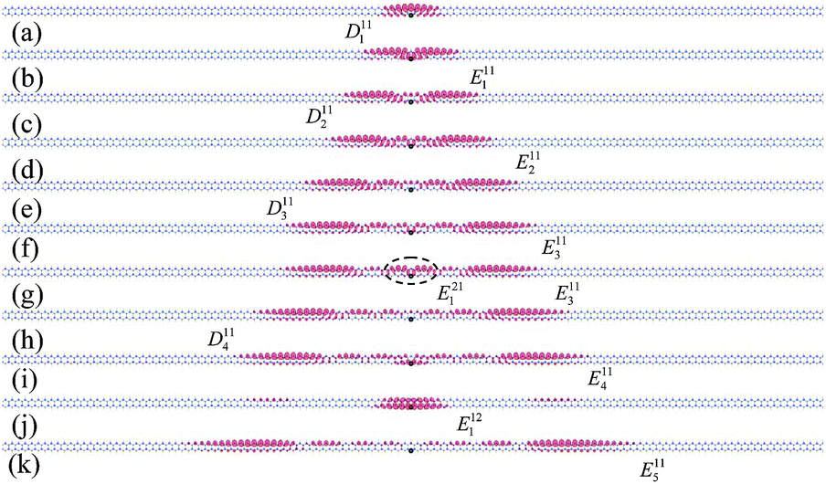 | ||
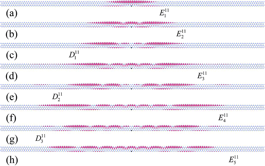
| Fig. 7 Exciton wave functions of 2-ZSiCNR for the first 10 lowest bright and dark excitons associated with the interband transitions E11, E21, and E12. (a) D111, (b) E111, (c) D211, (d) E211, (e) D311, (f) E311, (g) E221 and E311, (h) D411, (i) E411, (j) E112, and (k) E511. The bright and dark marks are under the incoming light polarization direction e‖Z. The hole (black spot) is fixed on top of a C atom (dark yellow spheres). The electron amplitude squared [|ΦS (re, rh = 0)|2 in arbitrary units (a.u.)] is shown by a red. | ||
 | ||
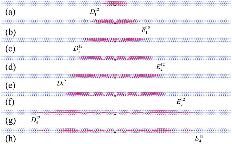
| Fig. 8 Exciton wave functions of 3-ZSiCNR for the first 8 lowest bright and dark excitons associated with the interband transitions E11. (a) E111, (b) E211, (c) D111, (d) E311, (e) D211, (f) E411, (g) D311, and (h) E511. The bright and dark marks are under the incoming light polarization direction e‖Z. The hole (black spot) is fixed on top of a C atom (dark yellow spheres). The electron amplitude squared [|ΦS (re, rh = 0)|2 in arbitrary units (a.u.)] is shown by a red. | ||
 | ||
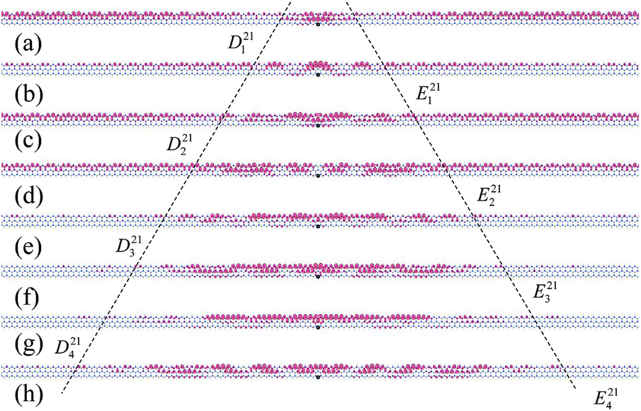
| Fig. 9 Exciton wave functions of 3-ZSiCNR for the first 8 lowest bright and dark excitons associated with the interband transitions E12. (a) D112, (b) E112, (c) D212, (d) E212, (e) D312, (f) E312, (g) D412, and (h) E412. The bright and dark marks are under the incoming light polarization direction e‖Z. The hole (black spot) is fixed on top of a C atom (dark yellow spheres). The electron amplitude squared [|ΦS (re, rh = 0)|2 in arbitrary units (a.u.)] is shown by a red. | ||
 | ||
| Fig. 10 Exciton wave functions of 3-ZSiCNR for the first 8 lowest bright and dark excitons associated with the interband transitions E21. (a) D121, (b) E121, (c) D221, (d) E221, (e) D321, (f) E321, (g) D421, and (h) E421. The bright and dark marks are under the incoming light polarization direction e‖Z. The hole (black spot) is fixed on top of a C atom (dark yellow spheres). The electron amplitude squared [|ΦS (re, rh = 0)|2 in arbitrary units (a.u.)] is shown by a red. | ||
It is clear that the wave functions plotted in Fig. 7–10 display a common feature of the exciton wave function, namely the spatial extent of the exciton wave function. The spatial extents of the excitons are closely related to their corresponding binding energies, i.e., the smaller the spatial extent of the exciton, the larger the exciton binding energy. Therefore, in the Eij series, the spatial extent of Enij, as well as that of Dnij, increases with n increasing. Taking Fig. 9 as an example, in the E12 series, the spatial extent of D112 is the smallest, which is the ground-state exciton, while the spatial extent of E512 is the largest. Therefore, the binding energy of the ground-state exciton is the largest in the same series of excitons, for example, the binding energy of D112 is the largest in the E12 series. Note that each 2-ZSiCNR in Fig. 7, as well as each 3-ZSiCNR Fig. 8–10, consists of 128 unit cells. It is clear that the extent of D111 of 2-ZSiCNR is smaller than that of E111 of 3-ZSiCNR, which indicates that the binding energy of D111 of 2-ZSiCNR is larger than that of E111 of 3-ZSiCNR. On the other hand, in the excitons of 3-ZSiCNR, the spatial extent of E121 is the smallest, then the extent of exciton E112 is smaller than that of exciton E111. Thus, the binding energy of exciton E121 is the maximum (0.786 eV), and the binding energy of exciton E112 (0.744 eV) is larger than that of exciton E111 (0.715 eV).
However, the exciton wave functions of N-ZSiCNR also display several unique characteristics. As shown in Fig. 7, 8, and 10, for the E11 and E21 series of excitons, one of the most striking characteristics is that the electron is confined to the Si edge while the hole is confined to the C edge, namely, the electrons and holes are separated spatially onto different edges. Such a kind of electron and hole spatial separation means that any of these excitons being formed gives rise to the fact that a charge transfer occurs in the system. Finally, such a charge transfer will affect the recombination time and diffusion processes of the electron–hole pairs. In contrast, the E12 series of excitons shows a different charge distribution. As shown in Fig. 9 and 7(j) (E112), the electron distribution of the E12 series of excitons is extended over the width of the ribbon, instead of being confined to one edge. What is the origin of such characteristics of electron distribution? From a previous study,21 we know that near the Z-point of the Brillouin zone, the first valence band originates from the pz atomic orbitals of the edge C atoms and the first conduction band originates from the pz atomic orbitals of the edge Si atoms, which are called the edge states. It is clear that En12 involving the electron state is the second conduction band, which does not belong to the edge state. In contrast, both E11 and E21 involving electron states are the first conduction band (Si edge), which is the edge state. As a result, the electron distribution of the E12 series of excitons is extended over the width of the ribbon, while for both the E11 and E21 series of excitons, the excited electron locates on the Si edge and the hole locates on the C edge. The E11 series of excitons are called the edge-state excitons, owing to the fact that the excited electron and hole result from edge states. Moreover, the edge-state excitons of N-ZSiCNR belong to charge-transfer excitons, owing to the fact that the excited electron and hole are confined to opposite edges.
It is very interesting to find a relationship between the node of the exciton wave functions and the incoming polarization light exciton excitation. We note that all exciton wave functions have symmetrical characteristics. In general, the wave functions of the excitons have nodes (zeros). In the Eij series, the nodes of the wave function of Enij, as well as those of Dnij, increase with n increasing. For example, as shown in Fig. 9, D112 is the ground state, and thus the wave function of D112 has no node. However, E112 is the first excited state, and thus the wave function has one node. D212 is the second excited state, and thus the wave function has two nodes, etc. On the other hand, under incoming light polarization direction e, whether an exciton is excited in the optical absorption spectrum or not is simply dependent on the odd or even number nodes of its wave function. If the exciton whose wave function possesses an even number of nodes is optically active, the exciton whose wave function possesses an odd number of nodes must be optically inactive and vice versa. For example, as shown in Fig. 9, the excitons whose wave functions possess an odd number of nodes are optically active, such as E112, E212, and E312, while the excitons whose wave functions possesss an even number of nodes are optically inactive, such as D112, D212, and D312, etc. However, when changing the light polarization from parallel (e‖Z) to perpendicular to the ribbon axis (e‖Y), the excitons whose wave functions possess an odd number of nodes are optically inactive, while the excitons whose wave functions possess an even number of nodes are optically active (refer to the marks of Fig. 6(c)).
The above relationship between the node of the exciton wave functions and the incoming polarization light exciton excitation can be understood further using an electric dipole moment model. It is noted that in eqn (6), 〈0|v|S〉 ≠ 0 is the electric dipole moment of the Sth exciton. That is to say, each exciton possesses a definitive electric dipole moment. On the other hand, due to its quasione-dimensional ribbon structure, there are two symmetrical directions in N-ZSiCNR; one is the longitudinal direction and another is the transverse direction. Thus, the dipole polar moment direction of the exciton is either transverse or longitudinal. Moreover, the electric dipole moment direction has a relationship with the node of the exciton wave function. For example, if the dipole polar direction of the wave function with an odd number of nodes is along the longitudinal direction, then the dipole moment direction of the wave function with an even number of nodes is perpendicular to the longitudinal direction (along the transverse direction). Therefore, in the longitudinal optical absorption spectra, the exciton of the wave function with an odd number of nodes is optically active (bright), while the exciton of the wave function with an even number of nodes is optically inactive (dark, dipole forbidden). In contrast, in the transverse absorption spectra, the exciton of the wave function with an odd number of nodes is optically inactive (dark, dipole forbidden), while the exciton of the wave function with an even number of nodes is optically active (bright).
It is noted that there is a dotted ellipse in Fig. 7(g), which marks out the region of the E121 wave function. From Table 2, we can see that the energy levels of E121 and E311 are 2.489 eV (see (b) and (d) of Fig. 3 and 4), namely, the degeneracy of the energy levels of E121 and E311. In order to compare the E121 + E311 wave function with the E311 wave function, as shown in Fig. 7(f), we also plot the E311 wave function. It is clear that the E121 + E311 wave function is different from the E311 wave function. Moreover, the binding energy of E311 is 0.422 eV, while the binding energy of E121 is 2.0586 (eV). However, both the E121 + E311 wave function and E311 wave function possess the same type of nodes, i.e., both E311 and E121 + E311 have an odd number of nodes. The E311 wave function has 5 nodes, E121 + E311 also has 5 nodes, and E121 has one node. Thus, when the incoming light polarization is parallel to the Z-axis, both E311 and E121 are optically active (bright exciton, refer to the marks of Fig. 3(b) and (d)). When changing the light polarization from parallel (e‖Z) to perpendicular to the ribbon axis (e‖Y), E311 becomes the optically inactive D311 (dark exciton, refer to the marks of Fig. 4(b)) and E121 becomes the optically inactive D121 (dark exciton, refer to the marks of Fig. 4(d)). As for the weight of the wave functions for E121 and E311 in Fig. 7(g), refer to ESI Table 1.†
Moreover, the degeneracy of the energy levels also occurs in the excitons of 3-ZSiCNR. It is noted that there are two auxiliary lines (drawn with dashed lines) in Fig. 10, which mark out the region of the E21 series exciton wave functions. As listed in ESI Table 2,† it is clear that there is energy level degeneracy between the E21 series excitons and the E11 series excitons. It is this degeneracy that give rise to the overlap between the E21 series exciton wave functions and the E11 series exciton wave functions. The weight of the wave functions for E21 and E11 in Fig. 10 are referred to in ESI Table 2.† For example, for Fig. 10(a), the weight of the wave function of the E11 series exciton (75th exciton) is 0.62481, while the weight of the wave function of the E21 series exciton (first exciton, i.e., D121) is 0.34912.
Lastly, we discuss the results that Alaal et al. recently obtained. It is noted that they found that the GW band gap of 2-ZSiCNR was 2.4 eV, which is larger than the HSE06 band gap (1.517 eV)36 but smaller than our obtained GW band gap (2.911 eV). For 3-ZSiCNR, their obtained GW band gap was 0.45 eV, which is almost equal to the HSE06 band gap (0.401 eV)36 and is almost half of our GW band gap (0.804 eV). Clearly their obtained GW band gaps are smaller than our obtained GW band gaps, particularly the GW band gap of 3-ZSiCNR. The differences between their results and our results originate from two facts. It is well known that the quasiparticle band gap from the GW calculations with or without the Coulomb truncation scheme can differ significantly. The Coulomb truncation scheme can remove image effects directly and leads to well converged results for modest-sized periodic cells, while in the scheme without Coulomb truncation, owing to the computational constraints, it is impossible to obtain a fully converged band gap simply by expanding the length of a vacuum region along the non-periodic direction.39,44,45 One fact is that in calculating the QP energies, we adopted the Coulomb truncation scheme, while Alaal et al. do not adopt the Coulomb truncation scheme. Another fact is that in calculating the QP energies, we adopted a 1 × 1 × 64 k-point grid, while Alaal et al. adopted a 1 × 1 × 32 k-point grid. Speaking specifically for the GW band gap of 3-ZSiCNR, the difference between our calculation results and the results from Alaal et al. originates from the above two facts. As for the GW band gap of 2-ZSiCNR, the difference between our calculation result and the results from mainly originates from the use of the Coulomb truncation scheme, because the GW band gap of 2-ZSiCNR with respect to a 1 × 1 × 32 k-point grid has been converged, while the GW band gap of 3-ZSiCNR does not (refer to ESI Table 3†).
On the other hand, as for the transverse absorption spectra, they found only one strongly bound exciton absorption peak in the transverse absorption spectra of the 2-ZSiCNR. Moreover, they fail to find any strongly bound exciton absorption peak in the transverse absorption spectra of the 3-ZSiCNR. However, we find that the optical absorption spectra of the 2-ZSiCNR and 3-ZSiCNR are dominated by edge-state-derived excitons with large binding energy, composed of a characteristic series of exciton states. The differences between the results from Alaal et al. and our results originate from three facts. The first fact is that in calculating the QP energies, we adopted the Coulomb truncation scheme, while Alaal et al. do not adopt the Coulomb truncation scheme. The second fact is that in calculating the QP energies, we adopted a 1 × 1 × 64 k-point grid, while Alaal et al. adopted a 1 × 1 × 32 k-point grid. These lead to the difference in the GW band gap, and therefore lead to the transverse absorption spectra difference. The third fact is that in calculating the kernel Keh, we not only adopted the Coulomb truncation scheme, but also adopted a coarse k-point grid of 1 × 1 × 64 and then interpolated onto a fine k-point grid of 1 × 1 × 256 to get converged exciton states,50,51 while Alaal et al. only adopted a 1 × 1 × 32 k-point grid. This directly leads to the transverse absorption spectra difference. Speaking specifically for the optical absorption spectra of the 3-ZSiCNR, that they fail to find any strongly bound exciton absorption peak in the transverse absorption spectra originates from the above three facts. As for 2-ZSiCNR, that they found only one strongly bound exciton absorption peak in the transverse absorption spectra mainly originates from the fact that they do not adopt the Coulomb truncation scheme, and the optical absorption spectra of the 2-ZSiCNR with respect to the 1 × 1 × 32 k-point grid has been converged, while the optical absorption spectra of the 3-ZSiCNR does not (referring to ESI Fig. 3–6†).
4 Conclusions
In summary, the electronic and optical properties of the 2-ZSiCNR and 3-ZSiCNR have been studied by means of first principles GW + BSE calculations. Quasi-particle GW self-energy corrections remarkably widened the corresponding Kohn–Sham band gaps: namely, the GW band gap of 2-ZSiCNR is 2.911 eV, which is more than three times larger than the Kohn–Sham band gap (0.957 eV), and the GW band gap of 3-ZSiCNR is 0.804 eV, which is more than nine times larger than the Kohn–Sham band gap (0.093 eV). By solving the BSE on top of the GW approximation, we demonstrated that the optical absorption spectra of the 2-ZSiCNR and 3-ZSiCNR are dominated by strong excitonic effects with the formation of strongly bound excitons. In the longitudinal optical absorption spectra, the binding energy of the first absorption peak exciton is 1.5 eV for 2-ZSiCNR and 0.8 eV for 3-ZSiCNR. However, in the transverse optical absorption spectra, the binding energy of the first absorption peak exciton of 2-ZSiCNR increases to 1.78 eV owing to the first absorption peak red shift, while the binding energy of the first absorption peak exciton of 3-ZSiCNR decreases to 0.464 eV owing to the first absorption peak blue shift. It is very interesting to find a relationship between the node of the exciton wave functions and the incoming polarization light exciton excitation. In the longitudinal optical absorption spectra, the exciton whose wave function possesses an odd number of nodes is optically active, while the exciton whose wave function possesses an even number of nodes is optically inactive. However, when changing the light polarization from parallel (e‖Z) to perpendicular to the ribbon axis (e‖Y), the exciton whose wave function possesses an odd number of nodes becomes optically inactive, while the exciton whose wave function possesses an even number of nodes becomes optically active. The rich physical properties of the 2-ZSiCNR and 3-ZSiCNR make them promising materials for photochemical catalysis, as well as for nanoscale photonic and optoelectronic devices. In addition, the above results may also provide valuable information for understanding the physical properties of other low-dimensional materials.Conflicts of interest
There are no conflicts to declare.Acknowledgements
This work was supported by the National Natural Science Foundation of China (grant no. 11174003) and the 211 Project of Anhui University.References
- Y.-W. Son, M. L. Cohen and S. G. Louie, Phys. Rev. Lett., 2006, 97, 216803 CrossRef PubMed.
- K. Nakada, M. Fujita, G. Dresselhaus and M. S. Dresselhaus, Phys. Rev. B: Condens. Matter Mater. Phys., 1996, 54, 17954 CrossRef CAS.
- M. Fujita, K. Wakabayashi, K. Nakada and K. Kusakabe, Peculiar, J. Phys. Soc. Jpn., 1996, 65, 1920–1923 CrossRef CAS.
- H. Lee, Y.-W. Son, N. Park, S. Han and J. Yu, Phys. Rev. B: Condens. Matter Mater. Phys., 2005, 72, 174431 CrossRef.
- Y.-W. Son, M. L. Cohen and S. G. Louie, Nature, 2006, 444, 347–349 CrossRef CAS PubMed.
- W. Y. Kim and K. S. Kim, Nat. Nanotechnol., 2008, 3, 408–412 CrossRef CAS PubMed.
- D. Yu, E. M. Lupton, M. Liu, W. Liu and F. Liu, Nano Res., 2008, 1, 56–62 CrossRef CAS.
- D. Yu, E. M. Lupton, H. J. Gao, C. Zhang and F. Liu, Nano Res., 2008, 1, 497–501 CrossRef CAS.
- Z. F. Wang, S. Jin and F. Liu, Phys. Rev. Lett., 2013, 111, 096803 CrossRef CAS PubMed.
- O. Hod, V. Barone, J. E. Peralta and G. E. Scueria, Nano Lett., 2007, 7, 2295–2299 CrossRef CAS PubMed.
- E.-J. Kan, Z. Li, J.-L. Yang and J. G. Hou, J. Am. Chem. Soc., 2008, 130, 4224–4225 CrossRef CAS PubMed.
- M. H. Wu, X. J. Wu and X. C. Zeng, J. Phys. Chem. C, 2010, 114, 3937–3944 CAS.
- D. Gunlycke, J. Li, J. W. Mintmire and C. T. White, Appl. Phys. Lett., 2007, 91, 112108 CrossRef.
- M. H. Wu, Y. Pei and X. C. Zeng, J. Am. Chem. Soc., 2010, 132, 5554–5555 CrossRef CAS PubMed.
- X. Chen, Y. Liu, B.-L. Gu, W. Duan and F. Liu, Phys. Rev. B: Condens. Matter Mater. Phys., 2014, 90, 121403(R) CrossRef.
- D. Krepel, J. E. Peralta, G. E. Scuseria and O. Hod, J. Phys. Chem. C, 2016, 120, 3791–3797 CAS.
- A. H. CastroNeto, F. Guinea, N. M. R. Peres, K. S. Novoselov and A. K. Geim, Rev. Mod. Phys., 2009, 81, 109–162 CrossRef CAS.
- L. Sun, Y. Li, Z. Li, Q. Li, Z. Zhou, Z. Chen, J. Yang and J. G. Hou, J. Chem. Phys., 2008, 129, 174114 CrossRef PubMed.
- E. Bekaroglu, M. Topsakal, S. Cahangirov and S. Ciraci, Phys. Rev. B: Condens. Matter, 2010, 81, 075433 CrossRef.
- J. M. Zhang, F. L. Zheng, Y. Zhang and V. Ji, J. Mater. Sci., 2010, 45, 3259–3265 CrossRef CAS.
- P. Lou and J. Y. Lee, J. Phys. Chem. C, 2009, 113, 12637–12640 CAS.
- P. Lou and J. Y. Lee, J. Phys. Chem. C, 2009, 113, 21213–21217 CAS.
- P. Lou and J. Y. Lee, J. Phys. Chem. C, 2010, 114, 10947–10951 CAS.
- P. Lou and J. Y. Lee, Bull. Korean Chem. Soc., 2012, 33, 763–769 CrossRef CAS.
- F.-L. Zheng, Y. Zhang, J.-M. Zhang and K.-W. Xu, Phys. Status Solidi B, 2011, 248, 1676–1681 CrossRef CAS.
- P. Lou, Phys. Chem. Chem. Phys., 2011, 13, 17194–17204 RSC.
- P. Lou, Phys. Status Solidi B, 2012, 249, 91–98 CrossRef CAS.
- P. Lou, J. Mater. Chem. C, 2013, 1, 2996–3003 RSC.
- P. Lou, Phys. Status Solidi B, 2014, 251, 423–434 CrossRef CAS.
- J. Guan, G. Yu, X. Ding, W. Chen, Z. Shi, X. Huang and C. Sun, ChemPhysChem, 2013, 14, 2841–2852 CrossRef CAS PubMed.
- X. Ding, G. Yu, X. Huang and W. Chen, Phys. Chem. Chem. Phys., 2013, 15, 18039–18047 RSC.
- W. Chen, H. Zhang, X. Ding, G. Yu, D. Liu and X. Huang, J. Mater. Chem. C, 2014, 2, 7836–7850 RSC.
- D. Liu, G. Yu, Y. Sun, X. Huang, J. Guan, H. Zhang, H. Li and W. Chen, Phys. Chem. Chem. Phys., 2015, 17, 941–950 RSC.
- H. Li, W. Chen, Y. Sun, X. Huang and G. Yu, Phys. Chem. Chem. Phys., 2015, 17, 24038–24047 RSC.
- D. D. Wu, H. H. Fu, L. Gu, Y. Ni, F. X. Zu and K. L. Yao, Phys. Chem. Chem. Phys., 2014, 16, 17493–17498 RSC.
- P. Lou, Phys. Status Solidi B, 2013, 250, 1265–1277 CrossRef CAS.
- N. Alaal, V. Loganathan, N. Medhekar and A. Shukla, Phys. Rev. Appl., 2017, 7, 064009 CrossRef.
- D. Y. Qiu, F. H. da Jornada and S. G. Louie, Phys. Rev. Lett., 2013, 111, 216805 CrossRef PubMed.
- H. C. Hsueh, G. Y. Guo and S. G. Louie, Phys. Rev. B: Condens. Matter, 2011, 84, 85404 CrossRef.
- L. Yang, Nano Lett., 2011, 11, 3844–3847 CrossRef CAS PubMed.
- P. Cudazzo, C. Attaccalite, I. V. Tokatly and A. Rubio, Phys. Rev. Lett., 2010, 104, 226804 CrossRef PubMed.
- J. Deslippe, M. Dipoppa, D. Prendergast, M. V. O. Moutinho, R. B. Capaz and S. G. Louie, Nano Lett., 2009, 9, 1330–1334 CrossRef CAS PubMed.
- L. Yang, J. Deslippe, C.-H. Park, M. L. Cohen and S. G. Louie, Phys. Rev. Lett., 2009, 103, 186802 CrossRef PubMed.
- L. Yang, M. L. Cohen and S. G. Louie, Phys. Rev. Lett., 2008, 101, 186401 CrossRef PubMed.
- L. Yang, M. L. Cohen and S. G. Louie, Nano Lett., 2007, 7, 3112–3115 CrossRef CAS PubMed.
- B. Arnaud, S. Lebègue, P. Rabiller and M. Alouani, Phys. Rev. Lett., 2006, 96, 026402 CrossRef CAS PubMed.
- V. Tran, R. Soklaski, Y. Liang and L. Yang, Phys. Rev. B: Condens. Matter, 2014, 89, 235319–235324 CrossRef.
- H. Shu, Y. Li, S. Wang and J. Wang, J. Phys. Chem. C, 2015, 119, 15526–15531 CAS.
- M. S. Hybertsen and S. G. Louie, Phys. Rev. B: Condens. Matter, 1986, 34, 5390 CrossRef CAS.
- J. Deslippe, G. Samsonidze, D. A. Strubbe, M. Jain, M. L. Cohen and S. G. Louie, Comput. Phys. Commun., 2012, 183, 1269–1289 CrossRef CAS.
- M. Rohlfing and S. G. Louie, Phys. Rev. B: Condens. Matter, 2000, 62, 4927 CrossRef CAS.
- P. Giannozzi, S. Baroni, N. Bonini, M. Calandra, R. Car, C. Cavazzoni, D. Ceresoli, G. L. Chiarotti, M. Cococcioni, I. Dabo, A. Dal Corso, S. Fabris, G. Fratesi, S. de Gironcoli, R. Gebauer, U. Gerstmann, C. Gougoussis, A. Kokalj, M. Lazzeri, L. Martin-Samos, N. Marzari, F. Mauri, R. Mazzarello, S. Paolini, A. Pasquarello, L. Paulatto, C. Sbraccia, S. Scandolo, G. Sclauzero, A. P. Seitsonen, A. Smogunov, P. Umari and R. M. Wentzcovitch, J. Phys.: Condens. Matter, 2009, 21, 395502 CrossRef PubMed.
- H. Ajiki and T. Ando, Jpn. J. Appl. Phys., 1995, 34(Suppl. 1), 107–109 CrossRef CAS.
- C.-H. Park, C. D. Spataru and S. G. Louie, Phys. Rev. Lett., 2006, 96, 126105 CrossRef PubMed.
- L. Yang, Phys. Rev. B: Condens. Matter, 2010, 81, 155445 CrossRef.
Footnote |
| † Electronic supplementary information (ESI) available: ESI Fig. 1 and 2 show the optical absorption spectra, where different Gaussian broadening δ has been used. ESI Table 1 lists the special analysis for exciton wave functions of the degeneracy energy levels of 2-ZSiCNR associated with the interband transitions Eij; ESI Table 2 lists the special analysis for exciton wave functions of the degeneracy energy levels of 3-ZSiCNR associated with the interband transitions Eij; ESI Table 3 lists the convergence of band gap energies Eg calculated by GW of N-SiCNRs with respect to the k-grid. ESI Fig. 3–6 show convergence of the optical absorption spectrum with respect to the k-grid. ESI Fig. 7 and 8 show the optical spectra in the polarizability per unit area. See DOI: 10.1039/c7ra09993b |
| This journal is © The Royal Society of Chemistry 2017 |