
 Open Access Article
 This Open Access Article is licensed under a
 Creative Commons Attribution 3.0 Unported Licence
Normal and abnormal dielectric relaxation behavior in KTaO3 ceramics
Lei Tong ,
Jie Sun,
Shuting Wang,
Youmin Guo,
Qiuju Li,
Hong Wang and
Chunchang Wang*
,
Jie Sun,
Shuting Wang,
Youmin Guo,
Qiuju Li,
Hong Wang and
Chunchang Wang*
Laboratory of Dielectric Functional Materials, School of Physics & Material Science, Anhui University, Hefei 230601, China. E-mail: ccwang@ahu.edu.cn
First published on 1st November 2017
Abstract
KTaO3 ceramic samples were prepared via a conventional solid state reaction route. The dielectric properties of KTaO3 were investigated in temperatures from room temperature to 1000 K and the frequency range of 102–106 Hz. The sample exhibits an abnormal dielectric behavior contrary to the traditional thermally activated behavior in the temperature range below 450 K. Our results revealed that the sample was very sensitive to humidity, leading to a metal-insulator transition (MIT) at 473 K. It is the positive temperature coefficient of resistance of the MIT that results in the abnormal dielectric behavior. When the temperature is higher than 500 K, the sample shows two normal dielectric relaxations following thermally activated behavior. The low- and high-temperature relaxations were argued, respectively, to be related to dipolar relaxation and Maxwell–Wagner relaxations due to oxygen vacancies hopping inside grains and then being blocked by grain boundaries.
1. Introduction
KTaO3 (KT for short) has been well-known as one of prototype incipient ferroelectric material, whose dielectric constant continuously increases with decreasing temperature and finally saturates to a plateau of ∼4000 at low enough temperatures (<10 K). This feature makes KT suitable for low-temperature applications. Due to this, a plethora of experimental and theoretical investigations have been performed on the low-temperature dielectric properties of KT.1–10 Among perovskite materials, the appealing dielectric properties of low dielectric loss and relatively high dielectric permittivity for KT make it attractive for study as a promising microwave material.11–14 On the other hand, KT crystal has highly polarizable lattice, which allows strong interaction of impurity-induced dipoles leading to dipole glass state15 and even to ferroelectric phase transition.16,17 Therefore, much attention has been paid to investigate the dielectric properties of KT induced by alien impurities.18–24However, compared with alien defects, the ubiquitous native point defects—oxygen vacancies (VOs) are widely known to be the “culprit” for various properties of perovskite oxides.25 In particular, VOs are capable to induce a polarized state in KT due to lattice distortion, as reported in other perovskites.26,27 Additionally, the migration and redistribution of VOs have been reported to play an important role in the degradation of ferroelectric devices.7,28 Therefore, fundamental knowledge of this kind of point defects in KT is of paramount importance. There are a number of theoretical reports concerning the VOs in KT.29–31 In contrast to the theoretical work, only a few experimental studies on this respect were performed in thin film system.32,33 To date, however, there is a notable lack of experimental work on VOs in ceramic KT.
Since VOs are active at high enough temperatures, we herein performed detailed investigations on high-temperature (300 to 1080 K) dielectric properties of KT ceramics aiming at understanding the dynamic features of VOs in this material. We observed abnormal dielectric behavior around room temperature and two oxygen-vacancy-related dielectric relaxations at high temperatures. The mechanisms of these dielectric phenomena were discussed.
2. Experimental details
KT ceramic samples were prepared by the conventional solid-state reaction method as reported in ref. 34. The raw materials used in this work are K2CO3 (99.99%), Ta2O5 (99.99%), which were stored at 473 K for 10 h to completely remove any absorbed water. Stoichiometric powders were thoroughly mixed for 2 hours using a mortar and then calcined at 1100 K for 8 h. The resultant mixture was reground, pressed into pellets with a size of 14 mm in diameter and 1–2 mm in thickness and finally sintered at 1523 K for 2 h. Phase purity of the sintered pellets was characterized by X-ray powder diffraction (XRD) performed on a Rigaku SmartLab diffractometer (Rigaku Beijing Co., Beijing, China) with Cu Kα radiation. Dielectric properties in both temperature and frequency domains were measured using a Wayne Kerr 6500B precise impedance analyzer (Wayne Kerr Electronic Instrument Co., Shenzhen, China) with the sample mounted in a holder placed inside a PST-2000HL dielectric measuring system (Partulab Co., Wuhan, China). The temperature domain dielectric properties were measured at fixed frequencies by varying temperature with a heating ramp of 2 K min−1. The frequency domain dielectric properties were measured at fixed temperatures by scanning frequency from 102 to 106 Hz. The ac measuring signal was 100 mV. Electrodes were made by printing silver paste on both sides of the disk-type samples. Annealing treatments were performed at 1073 K for 2 h in high purity (>99.99%) O2 or N2 with a flowing rate of 200 mL min−1.3. Results and discussions
3.1 Structure and microstructure characterization
Fig. 1 shows the typical room-temperature XRD pattern of KT ceramic sample in the 2θ range of 20 to 80°. The pattern can be indexed based on a cubic structure with Pm![[3 with combining macron]](https://www.rsc.org/images/entities/char_0033_0304.gif) m space group (JCPDS file no. 77-0918). No impurity phases were observed indicating the sample was identified to be single phase within the resolution of the equipment. The SEM image of the surface morphology of KT was shown in the insert of Fig. 1. It can be seen that the sample presents relatively uniform surface structure composed of particle with an average size about 0.5–1 μm together with small pores (with the size less than 0.5 μm).
m space group (JCPDS file no. 77-0918). No impurity phases were observed indicating the sample was identified to be single phase within the resolution of the equipment. The SEM image of the surface morphology of KT was shown in the insert of Fig. 1. It can be seen that the sample presents relatively uniform surface structure composed of particle with an average size about 0.5–1 μm together with small pores (with the size less than 0.5 μm).
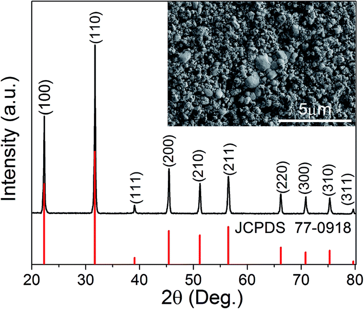 | ||
| Fig. 1 The XRD pattern of the KT sample recorded at room temperature. The insert shows SEM surface morphology. | ||
3.2 Normal dielectric behavior of ceramic KT
Fig. 2 summarizes the dielectric properties of a same KT pellet measured in the cases of as-prepared (a–c), after being annealed in O2 (d–f), and N2 (g–i) atmospheres. In the as-prepared case, the temperature (T) dependence of the dielectric constant, ε′(T), exhibits two weak step-wise increases as indicated by the arrows [Fig. 2(a)]. Since the step-wise increase in ε′(T) is always associated with dielectric relaxation, the finding implies that there might be two relaxations in the sample. However, the dielectric loss tangent, tan![[thin space (1/6-em)]](https://www.rsc.org/images/entities/char_2009.gif) δ(T), shows a broad shoulder without no clear signals of relaxation [Fig. 2(b)]. This result indicates that the relaxations might be shadowed by background. In order to eliminate the background, the dielectric function of electric modulus, defined as M* = M′ + jM′′ = 1/ε* is applied. It was reported that the electric modulus could effectively disclose the relaxation obscured by the background.35 Fig. 2(c) shows the temperature dependence of the electric modulus. From which two dielectric regions (I and II) can be classified. In region I, owing to the absence of background, the modulus spectra, M′′(T), reveal a set of pronounced relaxation peaks. The peak position shifts to higher temperature as the measured frequency increases indicating that the relaxation follows a thermally activated behavior. In region II, M′′(T) also shows a set of relaxation peaks. However, contrary to the thermally activated behavior, the peak position moves to lower temperature as the measuring frequency increases. To clearly discuss the different dielectric behaviors, the relaxation in region I is named as normal dielectric relaxation (NDR), whereas the relaxation in region II is named as abnormal dielectric relaxation (ADR). In this section, we focus on the mechanism of the NDR. The physics of the ADR will be discussed in next section.
δ(T), shows a broad shoulder without no clear signals of relaxation [Fig. 2(b)]. This result indicates that the relaxations might be shadowed by background. In order to eliminate the background, the dielectric function of electric modulus, defined as M* = M′ + jM′′ = 1/ε* is applied. It was reported that the electric modulus could effectively disclose the relaxation obscured by the background.35 Fig. 2(c) shows the temperature dependence of the electric modulus. From which two dielectric regions (I and II) can be classified. In region I, owing to the absence of background, the modulus spectra, M′′(T), reveal a set of pronounced relaxation peaks. The peak position shifts to higher temperature as the measured frequency increases indicating that the relaxation follows a thermally activated behavior. In region II, M′′(T) also shows a set of relaxation peaks. However, contrary to the thermally activated behavior, the peak position moves to lower temperature as the measuring frequency increases. To clearly discuss the different dielectric behaviors, the relaxation in region I is named as normal dielectric relaxation (NDR), whereas the relaxation in region II is named as abnormal dielectric relaxation (ADR). In this section, we focus on the mechanism of the NDR. The physics of the ADR will be discussed in next section.
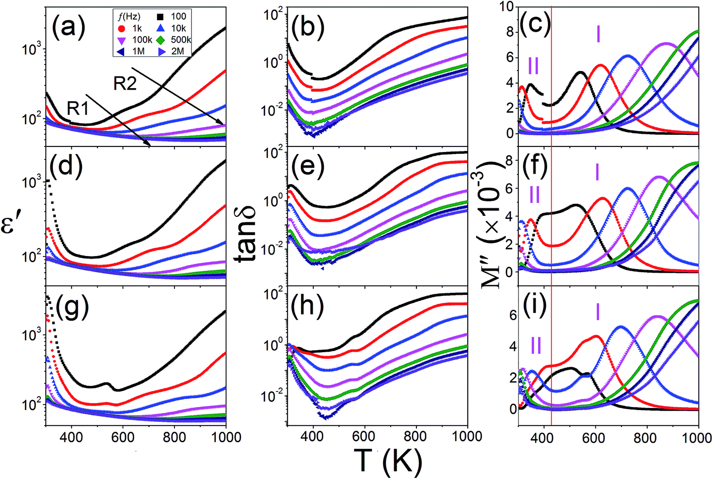 | ||
| Fig. 2 The dielectric properties of KT measured in the cases of as-prepared (a–c), after being annealing in O2 (d–f), and N2 (g–i) atmospheres. | ||
The NDR appears in the temperature range of T > 420 K. It has been reported that relaxations in perovskites in this high temperature range are exclusively related to VOs.36 To clarify this point, the same pellet used in Fig. 2 was subjected to two consecutive post-annealing treatments: first in O2 and then in N2 atmospheres. After each treatment, dielectric properties were measured as a function of temperature and the results were displayed in Fig. 2(d–f) and (g–i), respectively. Although, the O2- and N2-treatments lead to no remarkable changes in ε′(T) and tanδ(T), the modulus spectra, especially for the N2-annealed case, revel two NDRs in region I. For brevity, the two relaxations are referred to as R1 and R2 in the order of ascending temperature. The two NDRs can be identified in the curves measured with lower frequencies, e.g., 102 and 103 Hz, but can not be distinguished in the curves measured with frequency higher than 10 kHz. This indicates that the two relaxations have closed relaxation parameters. To calculate these parameters, we resort to the frequency domain.
Fig. 3(a) presents the spectroscopic plots of M′′(f) measured at the temperatures ranging from 473 to 773 K with an interval of 20 K. Though the modulus spectra show a set of pronounced relaxation peaks, a careful examination reveals that the M′′(f) curves are asymmetric. This is confirmed by the normalized plot as shown in Fig. 3(b), therein, the normalized electric modulus peak (M′′/M′′max) recorded at 573 K was plotted as a function of the reduced temperature (T/TP) with M′′max and TP being the peak intensity and position, respectively. It is found that the half value of full width at half maximum (FWHM) in the negative part of the peak is 0.82, which is lower than 0.93 of the positive part. This fact indicates that there still exists another weak peak in the high-frequency range, which is shadowed by the pronounced M′′(f) peak. To obtain the accurate peak position, the curve of M′′(f) was fitted using two Gaussian peaks. As an illustration, Fig. 3(c) shows the fitting result to the experimental data of M′′(f) measured at 513 K. The measuring temperature and the peak position (fP) for both relaxations deduced from the fittings were was plotted according to the Arrhenius law:
|
fP = f0exp(−Ea/kBT)
| (1) |
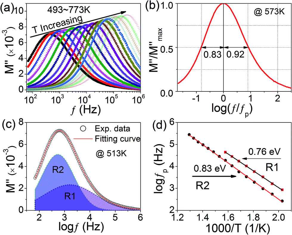 | ||
| Fig. 3 (a) Frequency dependence of the imaginary part of the electric modulus for the KT from 493 to 773 K with an interval of 20 K. (b) The normalized modulus vs. the reduced frequency (in log scale) at 573 K. (c) A representative example showing the comparison between the experimental data (open circles) measured at 513 K and fitting result (solid curve) as well as the resulting peaks (dashed curves). (d) The Arrhenius plots of R1 and R2 with the solid lines being the fitting results. | ||
It was reported that the activation energy of VO-related relaxation increases (decreases) with the decreasing (increasing) concentration of VOs38 which can be decreased (increased) by annealing in oxygen (nitrogen). To identify this point, the relaxation parameters (Ea and f0) were calculated in the O2-and then in N2-annealed cases. Table 1 summaries the values of the relaxation parameter of R1 and R2 in different measuring cases. From which, the values of activation energy for both relaxations are found to be increased by the O2-annealing treatment and then decreased by the N2-annealing treatment. This result firmly confirms that the two relaxations are associated with oxygen vacancies. The origin of VOs in KT can be reasonable ascribed to be the oxygen loss during the high temperature sintering process. Because oxygen is unavoidable in perovskite oxides, especially under a high firing temperature.39 Our recent results revealed that the hoping motion of VOs first created a dipolar relaxation and then a Maxwell–Wagner relaxation when the vacancies were blocked by interfaces such as grain boundaries.37 The observed relaxations, R1 and R2, can be ascribed to be the dipolar relaxation inside grains and Maxwell–Wagner relaxation due to grain boundaries, respectively. In order to evidence this point, we conduct impedance analysis.
| Annealing case | R1 | R2 | ||
|---|---|---|---|---|
| Ea (eV) | f0 (Hz) | Ea (eV) | f0 (Hz) | |
| As-prepared | 0.76 | 6.32 × 10¹⁰ | 0.83 | 1.51 × 10¹⁰ |
| O2-annealed | 0.81 | 5.11 × 10¹⁰ | 0.89 | 1.31 × 10¹⁰ |
| N2-annealed | 0.74 | 6.47 × 10¹⁰ | 0.81 | 1.08 × 10¹⁰ |
Fig. 4(a) displays the Nyquist plot (Z′′ vs. Z′, where Z′ and Z′′ are the real and imaginary parts of the complex impedance Z*) of KT recorded at the temperatures ranging from 573 to 693 K. The complex impedance spectra were analyzed using an equivalent circuit model. Empirically, the phenomenological constant phase element (CPE), which is a capacitive element with non-Debye behavior, is used to replace the ideal capacitor with Debye behavior due to the imperfect blocking characteristics of grain boundary and/or sample–electrode interface.40,41 Considering the impedance data, it can be best modeled by invoking an equivalent circuit consisting of two serially connected R-CPE units (R = resistor) shown in the inset of Fig. 4(a). The resistances of the grain and grain boundary of KT at different temperatures are obtained from the above analyses, and the results are shown in Fig. 4(b). The resistance is plotted as a function of the reciprocal temperature, and it well obeys the Arrhenius relaxation:
|
R = R0exp(−Econd/kBT)
| (2) |
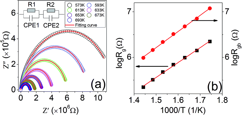 | ||
| Fig. 4 (a) Complex impedance plots and corresponding fitting results (solid curves) of KT at sever temperatures. The insert shows the equivalent circuits used for the fittings. (b) The Arrhenius plots for grain and grain boundary resistances deduced from the fittings. The straight lines are the linear-fitting results. | ||
3.3 Abnormal dielectric behavior of ceramic KT
To clearly evidence the abnormal dielectric behavior, detailed modulus spectra of KT in the as-prepared, O2-, and N2-annealed cases were measured in the temperature range from RT to 773 K. The results were shown, respectively, in Fig. 5(a)–(c). The modulus peak in all cases was found to first shift towards low frequency and then towards high frequency with increasing measuring temperature. Fig. 5(d) displays the Arrhenius curves for the three cases by plotting the peak position (fP) against the reciprocal of the measuring temperature. For the as-prepared case, a V-shaped Arrhenius curve is obtained. The data of both high- and low-temperature wings can be perfectly described by the Arrhenius law with positive and negative activation energy values indicative of NDR and ADR, respectively. In the O2-annealed case, only one data point for ADR was seen indicating that the ADR shifts towards lower temperature range by the treatment. In the N2-annealed case, more data point for ADR can be seen indicating that the ADR moves back to higher temperature range after N2-annealing treatment. These results imply that the ADR is closely related to VOs.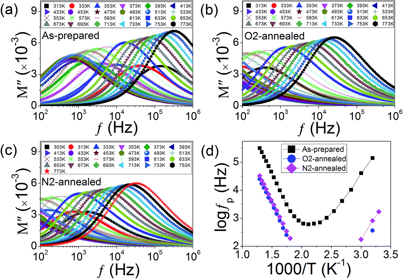 | ||
| Fig. 5 The dielectric modulus spectra of KT obtained in the (a) as-prepared, (b) O2-, and (c) N2-annealed cases. (d) The Arrhenius curves for the three cases by plotting the peak position (fP) against the reciprocal of the measuring temperature. | ||
There are literally few reports on ADR behavior. To the best of our knowledge, it was first found in ferroelectric ceramic BaTiO3 (ref. 42) and addressed to be related to VOs in BaTi0.85Zr0.15O3 by a Japanese group.39 Our group reported the ADR in laser crystals Gd2SiO5 and Yb-doped Gd2SiO5 and found that it was associated with a metal-insulator transition (MIT).43 We pointed out that the ADR was a corollary of the positive temperature coefficient of resistance (PTCR) of the MIT. Ferroelectric ceramics exhibit PTCR effect near the ferroelectric phase transition. The PTCR effect in non-ferroelectric Gd2SiO5 and Yb-doped Gd2SiO5 was caused by oxygen vacancy ordering.43
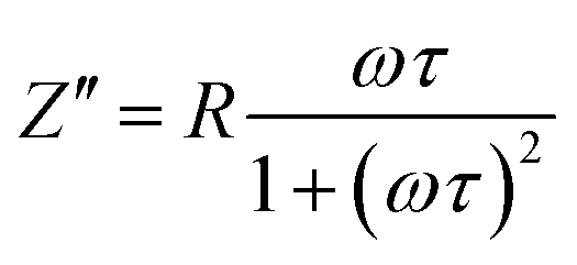
To find out whether or not the ADR in KT is associated with a MIT, we performed detailed impedance analysis on KT in the as-prepared, O2-, and N2-annealed cases and the corresponding results are illustrated in Fig. 6(a)–(c). At the lowest measuring temperatures, one notes that the impedance spectra in the frequency range f > 103 Hz for all cases behave as linear lines in the log–log representation. The data in the range of f < 103 Hz depart from the linear lines indicating that leaky current resulting from relaxation occurs. This departure leads to an impedance peak which can be modeled by an equivalent circuit composed of parallelly connected R–C (C = capacitor) elements as illustrated by the set of Fig. 6(d). Based on the circuit, the imaginary part of the impedance is given by
 | (3) |
 | ||
| Fig. 6 The impedance spectra of KT measured at different temperatures in the (a) as-prepared, (b) O2, and (c) N2-annealed cases. (d) Temperature dependence of the resistance of KT for the as-prepared, O2-, and N2-annealed cases. The insert shows an equivalent circuits in (d). | ||
It is well-known that potassium (K) is a very lively and volatile metal element. The volatilisation of K during high-temperature thermal process makes K-containing oxides very sensitive to humidity.44 Besides, the addition of alkali ion (K+) has been reported to be beneficial for improving the sensitivity of humidity.45 Zhen et al.46 pointed out that the humidity sensitivity was related to high mole content of hydrophilic group K–O bonds. The addition of alkali ions could create more surface defects and oxygen vacancies, resulting in an increase of the number of adsorption sites for water molecules. This background provides a heuristic hint that water vapor might be the principal cause of the ADR in KT.
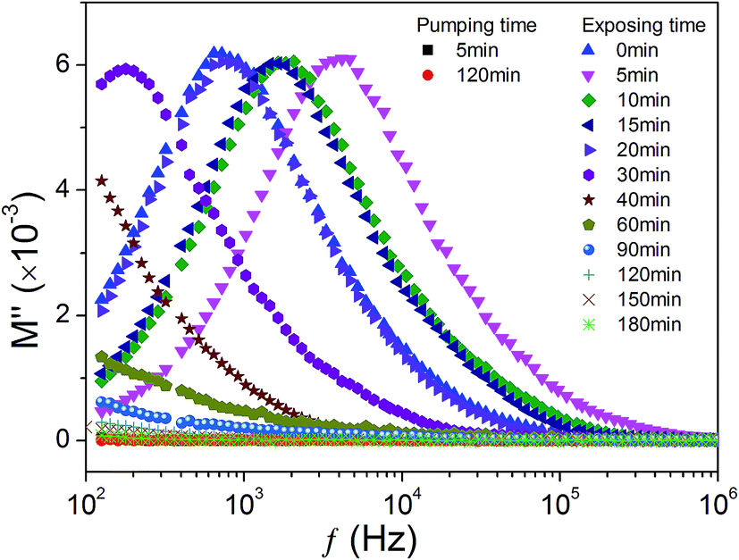
To elucidate this point, in Fig. 7 we recorded the change of electric modulus spectra at room temperature during the following consecutive processes: (1) we moved a KT pellet into the vacuum chamber of Janis SHI-4ST-1 closed cycle cryostat and started pumping, after 5 and 120 min, we recorded the frequency dependence of the modulus; (2) we opened the vacuum valve letting ambient air entering into the chamber and recorded the frequency dependence of the modulus at a series of time intervals. As seen from Fig. 7, when the sample was moved into vacuum chamber, the curve modulus almost dose not change with frequency and time. However, after exposing to ambient air, the modulus immediately shows a pronounced peak. The peak position was found to shift to high frequency with increasing exposing time. After exposing a short time of 5 min, the peak moves to low frequency with time increasing. This finding indicates that KT is very sensitive to humidity, which makes it suitable for humidity-sensitive material. After 30 min, only the high-frequency wing of the peak can be seen indicating that the peak moves out off the measuring frequency window. After 120 min, modulus spectra are independent of both time and frequency. These results firmly demonstrate that the appearance and disappearance of the electric modulus peak are related to the water adsorption and desorption in the sample, i.e., the variation of surrounding humidity. It, therefore, follows that the ADR in KT is induced by water vapor.
 | ||
| Fig. 7 The dielectric modulus spectra measured in closed vacuum chamber at room temperature during pumping and exposing processes. | ||
It is noteworthy that an non-Debye dielectric relaxation caused by water vapor in porous silica glasses has been extensively investigated by the group of Feldman.47–50 The non-Debye dielectric relaxation they called is actually the ADR termed herein. To describe this unusually relaxation they suggested a complicated relaxation time given by
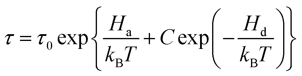 | (4) |
To check whether or not eqn (4) works in the present case, the relaxation time was deduced from the modulus spectra in the as-prepared case as shown in Fig. 5(a). Based on the R–C circuit, the modulus is given by
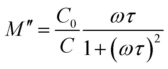 | (5) |
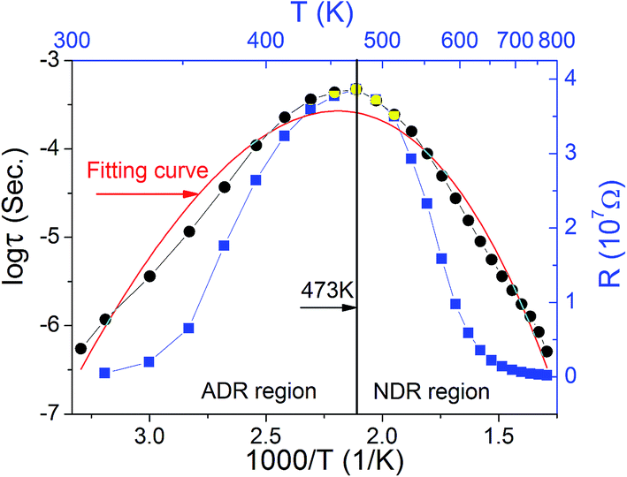 | ||
| Fig. 8 Comparison between the deduced relaxation time (black circles) and the fitting result based on eqn (4) (red line) as well as the resistance for KT recorded in the as-prepared case (blue square). | ||
As aforementioned that the ADR in non-ferroelectric materials is a corollary of PTCR effect. To decipher the relationship between the PTCR effect and ADR, the resistance data for the as-prepared KT pellet as shown in Fig. 5(a) were replotted in Fig. 8 for comparison. It is clearly seen that the temperature region of PTCR effect coincides with the ADR region. Therefore, the ADR results from the PTCR effect. This conclusion can be well understood based on the two facts: (1) since τ = RC, the capacitance as indicated by the modulus peak [see eqn (5)] slightly increases with increasing temperature as shown in Fig. 5(a). Thus, C can be treated as temperature-independent. The relaxation time is therefore determined by R. In the PTCR region, the relaxation time increases with increasing temperature giving rise to the ADR.
Let us focus on the origin of the PTCT effect. As aforementioned that the K-containing oxides is very sensitive to humidity. When water molecules are adsorbed by K+ ions, they subsequently transfer to OH− groups.46 The tested sample then is composed of relatively conductive surface layer and more insulating inner (bulk) part as illustrated in Fig. 9. The measured resistance can be modeled by two parallelly connected resistors: Rb for the bulk part and Rs for the surface layer. Therefore, the resistance is given by:
| 1/R = 1/Rs + 1/Rb | (6) |
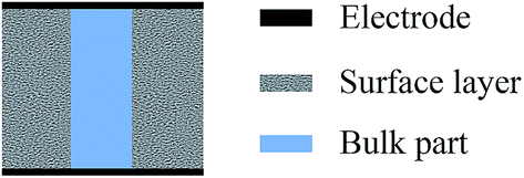 | ||
| Fig. 9 Ichnography illustration of the surface-layer structure of the tested cell. | ||
Since Rs < Rb, the resistance is dominated by the surface layer. Based on this fact, the observed ADR can be well explained: for the results obtained by varying temperature, more and more water molecules emit out off the sample as the measuring temperature increases. Thus, Rs increases with increasing temperature leading to PTCT effect, which, in turn, creates the ADR. For the results obtained varying time as shown in Fig. 7, when the sample is exposed to air, water absorption takes place immediately resulting in the surface layer. This leads to the rapid decrease of the resistance and moves the modulus peak into the frequency window. Elongating the exposing time means enlarging the surface layer volume and area (A), due to the adsorbed water penetrating into the inner part via meandering micropores. The capacitance of the surface layer given by
 | (7) |
4. Conclusions
In summary, we reported an anomalous dielectric behavior contrary to the traditional thermally activated behavior in KTaO3 ceramics in the temperature range below 450 K. Our results indicated that the abnormal dielectric behavior was associated with a metal-insulator transition induced by humidity. In the temperature range higher than 500 K, two sets of oxygen-vacancy-related relaxations (R1 and R2) were observed. The low-temperature relaxation was argued to be a dipolar relaxation caused by oxygen vacancies hopping inside grains and the high-temperature one was ascribed to be a Maxwell–Wagner relaxation due to the vacancies being blocked by grain boundaries.Conflicts of interest
There are no conflicts to declare.Acknowledgements
The authors thank financial support from National Natural Science Foundation of China (Grant No. 51502001). This work was supported in part by the Weak Signal-Detecting Materials and Devices Integration of Anhui University (Grant No. Y01008411).References
- Z. X. Chen, X. L. Zhang and L. E. Cross, J. Am. Ceram. Soc., 1983, 66, 511 CrossRef CAS.
- Z. Trybuła, S. Miga, S. Łoś, M. Trybuła and J. Dec, Solid State Commun., 2010, 209, 23 Search PubMed.
- A. K. Axelsson, M. Valant and N. M. Alford, J. Eur. Ceram. Soc., 2010, 30, 941 CrossRef CAS.
- B. Himmetoglu and A. Janotti, J. Phys.: Condens. Matter, 2016, 28, 065502 CrossRef PubMed.
- K. Rabe, C. H. Ahn and J. M. Triscone, Physics of ferroelectrics: a modern perspective, Springer, Berlin, 2007 Search PubMed.
- B. Salce, J. L. Gravil and L. A. Boatner, J. Phys.: Condens. Matter, 1994, 6, 4077 CrossRef CAS.
- G. A. Samara, J. Phys.: Condens. Matter, 2003, 15, R367 CrossRef CAS.
- Y. Uesu, H. Yokota, J. M. Kiat and C. Malibert, Ferroelectrics, 2007, 347, 37 CrossRef CAS.
- I. M. Smolyaninov, J. Phys.: Condens. Matter, 1998, 10, 10333 CrossRef CAS.
- A. R. Akbarzadeh, L. Bellaiche, K. Leung, J. Íñiguez and D. Vanderbil, Phys. Rev. B: Condens. Matter Mater. Phys., 2004, 70, 054103 CrossRef.
- R. G. Geyer, B. Riddle, J. Krupka and L. A. Boatner, J. Appl. Phys., 2005, 97, 104111 CrossRef.
- S. Glinśek, D. Nuzhnyy, J. Petzelt, B. Malič, S. Kamba, V. Bovtun, M. Kempa, V. Skoromets, P. Kužel, I. Gregora and M. Kosec, J. Appl. Phys., 2012, 111, 104101 CrossRef.
- A. K. Axelsson, Y. Pan, M. Valant and N. Alford, J. Am. Ceram. Soc., 2009, 92, 1773 CrossRef CAS.
- A. K. Axelsson, Y. Pan, M. Valant and N. M. Alford, J. Am. Ceram. Soc., 2010, 93, 800 CrossRef CAS.
- B. E. Vugmeister and M. D. Glinchuk, Rev. Mod. Phys., 1990, 62, 993 CrossRef CAS.
- D. Rytz, A. Châtelain and U. T. Höchli, Phys. Rev. B: Condens. Matter Mater. Phys., 1983, 27, 6830 CrossRef CAS.
- U. T. Höchli and L. A. Boatner, Phys. Rev. B: Condens. Matter Mater. Phys., 1979, 20, 266 CrossRef.
- S. A. Prosandeev, V. S. Vikhnin and S. E. Kapphan, J. Phys.: Condens. Matter, 2002, 14, 4407–4414 CrossRef CAS.
- Z. Trybuła, S. Miga, S. Łoś, M. Trybuła and J. Dec, Phys. Status Solidi B, 2016, 253, 1076 CrossRef.
- G. Geneste, J. M. Kiat, H. Yokota, Y. Uesu and F. Porcher, Phys. Rev. B: Condens. Matter Mater. Phys., 2010, 81, 144112 CrossRef.
- G. Geneste, J. M. Kiat, H. Yokota and Y. Uesu, Phys. Rev. B: Condens. Matter Mater. Phys., 2011, 83, 184202 CrossRef.
- A. K. Axelsson, Y. Pan, M. Valant, P. M. Vilarinho and N. M. Alford, J. Appl. Phys., 2010, 108, 064109 CrossRef.
- A. Levstik, C. Filipič, O. Bidault and M. Maglione, Phys. B Condens. Matter, 2008, 403, 3608 CrossRef CAS.
- E. L. Venturini, G. A. Samara, V. V. Laguta, M. D. Glinchuk and I. V. Kondakova, Phys. Rev. B: Condens. Matter Mater. Phys., 2005, 71, 094111 CrossRef.
- W. L. Warren, K. Vanheusden, D. Dimos, G. E. Pike and B. A. Tuttle, J. Am. Ceram. Soc., 1996, 79, 536 CrossRef CAS.
- B. Himmetoglu and A. Janotti, J. Phys.: Condens. Matter, 2016, 28, 065502 CrossRef PubMed.
- B. Salce, J. L. Gravil and L. A. Boatner, J. Phys.: Condens. Matter, 1994, 6, 4077 CrossRef CAS.
- R. G. Geyer, B. Riddle, J. Krupka and L. Boatner, J. Appl. Phys., 2005, 97, 104111 CrossRef.
- M. Choi, F. Oba and I. Tanaka, Phys. Rev. B: Condens. Matter Mater. Phys., 2011, 83, 214107 CrossRef.
- A. Shigemi, T. Koyama and T. Wada, Phys. Status Solidi C, 2006, 3, 2862 CrossRef CAS.
- S. G. Kang and D. S. Sholl, J. Chem. Phys., 2014, 141, 024707 CrossRef PubMed.
- D. A. Mota, Y. Romaguera-Barcelay, A. Tkach, J. Pérez de la Cruz, P. M. Vilarinho, P. B. Tavares, J. Agostinho Moreira and A. Almeida, J. Appl. Phys., 2013, 114, 034101 CrossRef.
- M. Tyunina, J. Narkilahti, M. Plekh, R. Oja, R. M. Nieminen, A. Dejneka and V. Trepakov, Phys. Rev. Lett., 2010, 104, 227601 CrossRef CAS PubMed.
- A. Tkach, A. Almeida, J. Agostinho Moreira, J. Perez de la Cruz, Y. Romaguera-Barcelay and P. M. Vilarinho, Appl. Phys. Lett., 2012, 100, 192909 CrossRef.
- C. C. Wang, J. Wang, X. H. Sun, L. N. Liu, J. Zhang, J. Zheng and C. Cheng, Solid State Commun., 2014, 179, 29 CrossRef CAS.
- C. C. Wang, C. M. Lei, G. J. Wang, X. H. Sun, T. Li, S. G. Huang, H. Wang and Y. D. Li, J. Appl. Phys., 2013, 113, 094103 CrossRef.
- C. C. Wang, M. N. Zhang, K. B. Xu and G. J. Wang, J. Appl. Phys., 2013, 112, 034109 CrossRef.
- S. Steinsvik, R. Bugge, J. O. N. Gjønnes, J. Taftø and T. Norby, J. Phys. Chem. Solids, 1997, 58, 969 CrossRef CAS.
- J. Xu and M. Itoh, Chem. Mater., 2005, 17, 1711 CrossRef CAS.
- R. Schmidt, W. Eerenstein, T. Winiecki, F. D. Morrison and P. A. Midgley, Phys. Rev. B: Condens. Matter Mater. Phys., 2007, 75, 245111 CrossRef.
- K. R. S. Preethi Meher and K. B. R. Varma, J. Appl. Phys., 2009, 105, 034113 CrossRef.
- D. C. Sinclair and A. R. West, J. Appl. Phys., 1989, 66, 3850 CrossRef CAS.
- L. N. Liu, C. C. Wang, D. M. Zhang, Q. L. Zhang, K. J. Wang, J. Wang and X. H. Sun, J. Am. Ceram. Soc., 2014, 97, 1823 CrossRef CAS.
- C. W. Ahn, S. Y. Lee, H. J. Lee, A. Ullah, J. S. Bae, E. D. Jong, B. H. Park and I. W. Kim, J. Phys. D: Appl. Phys., 2009, 42, 215304 CrossRef.
- Z. Wang, C. Chen, T. Zhang, H. Guo, B. Zou, R. Wang and F. Wu, Sens. Actuators, B, 2007, 126, 678 CrossRef CAS.
- Y. H. Zhen, M. M. Wang, S. Wang and Q. Z. Xue, Ceram. Int., 2014, 40, 10263 CrossRef CAS.
- Y. Feldman, A. Puzenko and Y. Ryabov, Chem. Phys., 2002, 284, 139 CrossRef CAS.
- A. Gutina, T. Antropova, E. Rysiakiewicz-Pasek, K. Virnik and Y. Feldman, Microporous Mesoporous Mater., 2003, 58, 237 CrossRef CAS.
- A. Gutina, E. Axelrod, A. Puzenko, E. Rysiakiewicz-Pasek, N. Kozlovich and Y. Feldman, J. Non-Cryst. Solids, 1998, 235, 302 CrossRef.
- Y. Ryabov, A. Gutina, V. Arkhipov and Y. Feldman, J. Phys. Chem. B, 2001, 105, 1845 CrossRef CAS.
| This journal is © The Royal Society of Chemistry 2017 |