
 Open Access Article
 This Open Access Article is licensed under a
 Creative Commons Attribution 3.0 Unported Licence
Unipolar resistive switching behavior in sol–gel synthesized FeSrTiO3 thin films
Atul Thakre ab,
Jyoti Kaswanab,
A. K. Shuklab and
Ashok Kumar*ab
ab,
Jyoti Kaswanab,
A. K. Shuklab and
Ashok Kumar*ab
aAcademy of Scientific and Innovative Research (AcSIR), CSIR-National Physical Laboratory Campus, Dr. K. S. Krishnan Marg, New Delhi 110012, India. E-mail: ashok553@nplindia.org
bCSIR-National Physical Laboratory, Dr. K. S. Krishnan Marg, New Delhi 110012, India
First published on 24th November 2017
Abstract
A robust unipolar resistive switching (URS) was successfully observed in sol–gel derived perovskite type Fe-doped strontium titanate (FeSTO) thin films, deposited on an ITO-coated glass substrate by a spin-coating technique. The surface topography of the films was characterized by atomic force microscopy that suggested a smooth surface with an average surface roughness nearly 1–2 nm. The crystal structure, URS phenomena, current–voltage characteristics, and dielectric and impedance behavior were analyzed for both high resistance state (HRS) and low resistance state (LRS). The X-ray photoelectron spectroscopy (XPS) was also employed to investigate the valence states of the host and dopants elements. The Au/FeSTO/ITO device offers a large resistance ratio of HRS and LRS (Roff/Ron) around 105, long stable retention characteristics for 104 s, and a distinguished and large non-overlapping voltage window of ∼4 to 6 V for SET and RESET operations.
Introduction
Since last five decades, the scaling performance of microelectronics successfully meets the prediction of Moore's law of doubling of transistors after two years. However, now, it has been realized that due to the physical limits in the scaling of the silicon-based devices, it will be difficult to follow the Moore's law. In this regard, various crystalline and amorphous materials have received significant interest due to the presence of resistive switching (RS) properties that offer several advantages, such as higher scaling, very simple cross-bar structure, lower power consumption, fast operation, and capability, over the Si-based memory devices to meet the criteria beyond the Moore's law.1,2 Multilevel resistive states or analogous resistive states of the RS memory devices can also be referred as memristors.3,4 The RS phenomena are controlled by a defect-driven process that is based on the changes in the resistance states (high to low or vice versa) under the external stimulus of an electric field.5 The transition between two or more (in multilevel resistive switching devices) resistive states can be employed as the resistive random access memory (ReRAM)6 elements or the electronic switches in microelectronic circuit applications. There are two different switching phenomena that exist in the systems depending on the polarity of the stimulus voltage: bipolar resistive switching (BRS) and unipolar resistive switching (URS).7 BRS provides a faster switching speed, a very low operation power, and an easy switch from one state to another state, whereas URS shows a larger ON/OFF ratio and a better scaling capability.8 The microscopic mechanisms responsible for the change in the resistive state of the device are still a matter of debate and quiet dependent on the material combination and its interface with different work function electrodes. Several models, such as migration of oxygen vacancies, metallic filament formation, and cationic migrations, have been proposed to explain the switching phenomenon. From last few years, RS behavior in various organic9 and thin inorganic films,5 such as graphene oxide,10 various binary and complex compounds, such as TiO2,11,12 NiO,13 ZnO,14 titanates,15 and zirconates,16 has been reported. In case of binary oxides, various scientific groups have reported the BRS behavior,17,18 whereas in case of the perovskite materials, both BRS and URS behaviors have been observed depending upon the applied electric field strength and various ranges of the compliance current.19 Several studies on the RS phenomena in SrTiO3 have been reported. An STO is a popular perovskite oxide due to its multifunctional physical and chemical properties such as photo-catalytic properties, superconductivity, thermal stability, and higher dielectric constant.20–23 The pure STO is an electrical insulator with a large band gap of ∼3.2 eV. However, the electrical conductivity of the STO can be altered by tailoring its compositional design. Due to this, the RS phenomena in the STO have been widely studied for the future generation non-volatile RAM applications. Filamentary types of the RS phenomena have been reported when active electrodes, such as Ag and Cu, were used.24 In the case of the inert metal electrodes such as Au and Pt, oxygen vacancies were introduced to attain resistive switching. These oxygen vacancies were generated by different methods such as incorporating doping elements such as Fe25 and Cr,26 ultraviolet irradiation while measuring the switching effect,27 and thermal treatment.28,29 Both filamentary and non-filamentary RS phenomena have been reported for the STO system. Filamentary and non-filamentary types of the RS phenomenon were observed mainly because of the accumulation of the oxygen vacancies inside the STO thin film and near the interface of the electrode–dielectric.25,30–32 Muenstermann et al.25 reported the coexistence of filamentary and homogeneous BRS behaviour in the 1% Fe-doped STO thin films fabricated on a Nb:STO substrate by pulsed laser deposition (PLD) technique. Similarly, Lenser et al.33,37 demonstrated a flimsy resistive switching in the less than 5% Fe-doped STO thin films grown by PLD with a small Roff/Ron ratio.Among these studies on the RS phenomena in strontium titanate, most were limited to a single crystal, epitaxial thin films, and pure SrTiO3 fabricated by the expensive and complex physical deposition techniques. On the other hand, solution-based methods provide a very inexpensive and easy way to synthesize and fabricate oxide thin films. In this study, we present a very stable and robust unipolar resistive switching (URS) behavior in a sol–gel synthesized perovskite Fe-doped SrTiO3 thin film deposited by a spin coating technique on an ITO electrode.
Experimental details
The Fe-STO thin films were prepared by the spin-coating technique. The solutions were prepared by a sol–gel method. The sol–gel method is a chemical synthesis method having several advantages such as relatively simple, ease of control over the compositional stoichiometry, lesser impurities, and economical. To prepare the FeSTO solution, strontium acetate (SrC4H6O4·1/2H2O) and titanium IV isopropoxide (Ti[OCH(CH3)2]4) were used as precursors. Acetic acid and 2-methoxy ethanol were used as solvents. Initially, a solution (called solution A) of acetic acid and 2-methoxy ethanol having a ratio of 1![[thin space (1/6-em)]](https://www.rsc.org/images/entities/char_2009.gif) :1 was prepared. Then, a calculated amount of strontium acetate was dissolved in solution A and stirred for half an hour with heating at 50 °C till it formed a transparent solution. Later, a calculated amount of titanium isopropoxide and iron pentanoate (C15H27FeO6) was added separately in a 19:1 ratio for Fe doping of 5 mol% concentration. Titanium isopropoxide was added drop by drop by a micropipette while stirring the solution, followed by stirring for 5 h in a closed flask.
:1 was prepared. Then, a calculated amount of strontium acetate was dissolved in solution A and stirred for half an hour with heating at 50 °C till it formed a transparent solution. Later, a calculated amount of titanium isopropoxide and iron pentanoate (C15H27FeO6) was added separately in a 19:1 ratio for Fe doping of 5 mol% concentration. Titanium isopropoxide was added drop by drop by a micropipette while stirring the solution, followed by stirring for 5 h in a closed flask.
The indium tin oxide (ITO)-coated glass slides were used as substrates. Initially, the 10 mm × 10 mm substrates were cleaned with acetone for two minutes and later by isopropyl alcohol for 10 minutes. The spin coater NXGM1 model was used for the thin film preparation at 5000 rpm for 30 s. The obtained thin films were annealed at 700 °C for one hour. For the electrical measurements, the top Au electrode was deposited through a shadow mask, having a diameter of 200 μm and a thickness of 20 nm, by a DC sputtering technique. The electrical measurements were performed using a microprobe system and an optical microscope. All the current–voltage and impedance spectroscopy measurements were performed using Agilent B2901a and Hioki 3532-50 LCR HiTester, respectively. The impedance spectroscopy measurements were performed with an oscillation voltage of 0.5 V and frequency ranges from 100 Hz to 1 MHz. The surface topography and the crystal structure were investigated by atomic force microscopy and X-ray diffraction techniques. An ultra-high vacuum surface analysis system equipped with a monochromatic Al Kα/non-monochromatic Mg Kα X-ray source and an EA125 electron energy analyser was utilized to carry out the X-ray photoelectron spectroscopy (XPS) study. The C 1s (284.8 eV) core level was used for binding energy (BE) and charge correction.
Results and discussion
The XRD patterns of the FeSTO thin films coated on the ITO glass substrate annealed at 700 °C are shown in Fig. 1(a). The peaks at 32.3° and 47.4° corresponding to STO (110) and STO (200) of the FeSTO thin film are indexed properly using the pseudo-cubic crystal structure. The surface topography image of the FeSTO thin film is shown in Fig. 1(b). The topographical study of the films was performed using a Gwyddion software tool. The average film thickness is near ∼70 nm, as probed by the profilometer. The average grain sizes are in the range of ∼30 nm with an average surface roughness in the range from ∼1 to 2 nm. | ||
| Fig. 1 (a) The XRD data of the ITO coated glass substrate and the FeSTO thin film deposited on the ITO-coated glass substrate and (b) the AFM image of the top surface of the thin film. | ||
The energy band diagram for the Au/FeSTO/ITO resistive switching device is shown in Fig. 2(a). The energy band situation is for the FeSTO thin film with Au (work function is 5.1 eV) as the top electrode and ITO (work function is 4.4 eV)34 as the bottom electrode. The electron affinity of the FeSTO thin film is speculated to be ∼4.1 eV, as reported for STO.35,36 When the metal electrode and dielectric thin film is brought into contact, free charge carriers will flow until an equilibrium condition is achieved. In this electrode–dielectric interaction, due to a large work function of Au and FeSTO's n-type nature, a space charge depletion region and large barrier height are developed at the Au/FeSTO interface that forms a Schottky-type potential barrier.
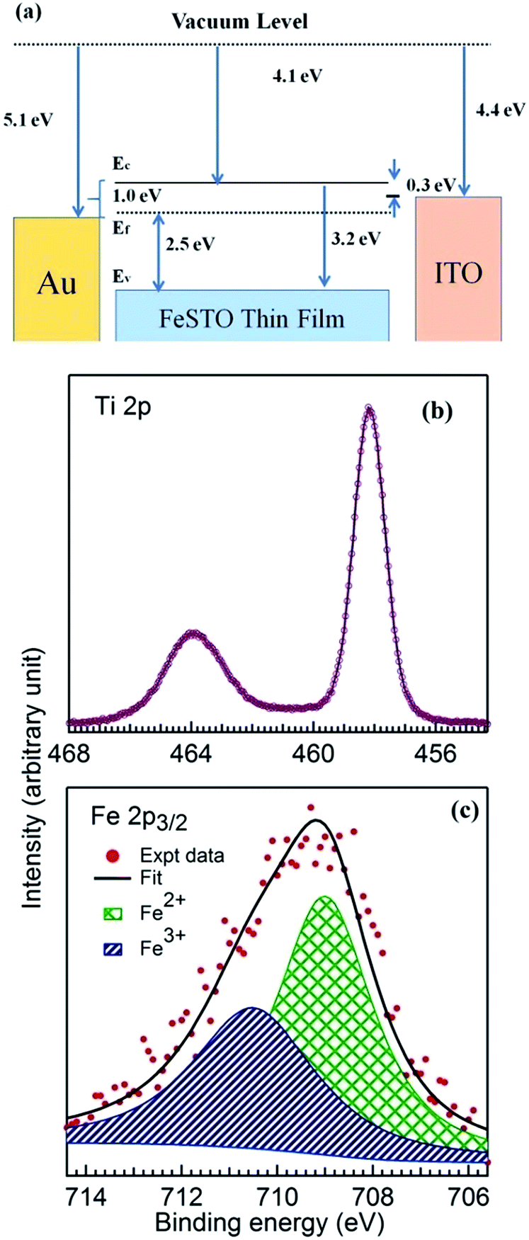 | ||
| Fig. 2 (a) The energy band diagram of the Au/FeSTO/ITO capacitive structure, (b) Ti 2p XPS core level, and (c) Fe 2p XPS core level (dots) along with fitting component (patterned). | ||
Similarly, due to a low work function of ITO, at the ITO/FeSTO interface, the barrier height is almost negligible (0.3 eV), and an ohmic contact may be possible. The barrier height varies with a change in the magnitude and direction of the applied electric field. When a positive voltage is applied to the top Au electrode, the electrode-FeSTO junction is forward biased that lowers down the Schottky barrier height. Initially, the memory device is in HRS, and after the positive potential is applied on the top Au electrode, the oxygen vacancies present in the FeSTO film37 are pushed downwards towards the bottom ITO electrode; this eventually results in the formation of a series of conducting paths into the oxide film. This conducting filamentary path formation results in the LRS of the memory device. Later, the voltage sweep with an increased compliance current (100 mA) is applied; the temperature of the previously formed filament increases with the increase in the passing current due to the Joule heating effect,38 which results in the rupturing of the filament and RESET of the device. The rupturing and filament formation process are not homogeneous for each cycle of SET and RESET process and a set of devices that intrinsically develops a memory voltage window for SET and RESET process.
The XPS measurements have also been performed to analyze the valence states of the host and doped elements, which are shown in Fig. 2(b) and (c). In Fig. 2(b), two peaks at 458.2 eV and 463.9 eV belong to the Ti 2p3/2 and Ti 2p1/2, respectively.39 These peaks correspond to the Ti4+ oxidation state. In Fig. 2(c), we have shown the Fe 2p core level of the 5% Fe-doped SrTiO3 thin film. The Fe 2p core level has been fitted with two nearly Gaussian components. The peaks located at 708.9 and 710.4 eV can be assigned to Fe2+ and Fe3+, respectively.40,41 The calculated area% for Fe2+ and Fe3+ is roughly 60% and 40%, respectively, which suggests the presence of significant mixed valence states of Fe. It may indicate the presence of oxygen vacancies in the FeSTO thin film. This scenario has also been suggested by Wan et al. in the Cr-doped STO thin films.42
In the RS behaviour testing process, the top Au electrode was kept positively biased, whereas the bottom ITO electrode was kept negatively biased. Initially, the pristine FeSTO devices are in HRS and have the resistance in ∼MΩ. For switching the device into LRS, an initial electroforming voltage (∼8.5 V) has been obtained. At first, we have increased the applied potential through the device, which abruptly increases at ∼8.5 V, which in turn develops current filaments (Fig. 3(a) and (b)). This switching process from HRS to LRS is called the SET process. To the SET the device, a voltage sweep from 0 V to 10 V with a fixed compliance current of 1 mA was applied. Most of the devices show a lower SET voltage as compared to the electroforming voltage. To RESET the device, again a voltage sweep from 0 V to 4 V with a compliance current of 100 mA was applied. When the applied potential approaches ∼2.5 V, the current through the device drops abruptly, and hence, the resistive state of the device changes from LRS to HRS (RESET process). Herein, the maximum drawing current in the LRS state is near ∼30 mA in each SET operation, which is acceptable for the NVRAM applications.
 | ||
| Fig. 3 (a) The I–V plot for the URS behavior of the Au/FeSTO/ITO memory device, (b) SCLC mechanism linear fitting for the URS behavior. (c) The retention characteristics and (d) the endurance characteristics of the FeSTO memory device. | ||
For the application point of view, charge retention and endurance characteristics of the FeSTO thin film devices are shown in Fig. 3(c) and (d), respectively. For the retention characteristic measurement, a very low constant potential of 0.5 V with a compliance current of 1 mA was applied across the device for both HRS and LRS, and the respective currents were obtained. The obtained current values are almost constant in both the HRS and LRS states over 104 s. It concludes that the device exhibits an excellent retention characteristic. To carry out the endurance characteristic test for the devices, consecutive multiple SET and RESET operations were performed for up to 50 cycles. Herein, the FeSTO devices have shown very stable and repetitive endurance characteristics.
The conduction mechanism is analyzed for the FeSTO thin films. For both LRS and HRS, the I–V data were re-plotted as logJ vs. logE and linearly fitted to investigate the space charge limited conduction (SCLC) mechanism for the resistive switching, as shown in Fig. 3(b). In the HRS state, for the lower applied field region (up to around 4V cm−1, in log scale), the slope value is nearly around ∼0.4, indicating a very high resistive state. Further increment in the applied electric field causes a gradual increment in the slope to 2.7; this indicates the space charge limited conduction (Child's law, I ∝ V2). The observed slope favours the trap-free SCLC conduction process. Later on, with a further increase in the applied potential, a free flow of sea of charge injection across both terminals of the devices takes place, which in turn results in the SET of the device, and the current approaches the compliance current; this indicates the formation of a conductive filament within the capacitive device, which dominates over the Schottky interface barrier between FeSTO and the top Au electrode. Thus, it signifies the filamentary resistive switching process. Similarly, for the LRS state, the measured slope of the logarithmic J–V characteristics is close to one, indicating an ohmic behavior. In the RESET process, the rupturing of the conducting filament can be explained by the Joule heating effect.43 The high passing current (around ∼30 mA) causes the increase in the temperature44 of the filament (∼800 K) and thus ruptures it at the reset voltage (VRESET). The relationship between the current density and the applied electric field is denoted by
| JSCLC = (9/8)μεθE2/d |
J vs. E1/2 and lnJ/E vs. E1/2 provide an unrealistic optical dielectric constant of the FeSTO.
The conduction mechanism is further explored by the impedance spectroscopy technique. In this measurement, after each SET and RESET operation, impedance, capacitance, phase angle, and tangent loss were determined in the frequency range from 100 Hz to 1 MHz at a constant AC voltage (0.5 V). The frequency response of capacitance and tangent loss are shown in Fig. 4(a) and (b), respectively. Fig. 4(a) shows that in the HRS region, the capacitance is almost linear and gradually decreases over the whole frequency range; this indicates a very high resistive device; on the other hand, for the LRS, the capacitance exponentially decreases in the lower frequency region and then gradually decreases in the higher frequency region. It indicates the presence of the formation of an ohmic conductive filament (CF) (free charge carriers), where Cp is decreasing with an increase in the frequency. The capacitance of the devices is almost the same for both HRS and LRS above 1 kHz probe frequencies; however, at the same time, these devices show many folds increase in tangent loss. These results suggest the formation of the conducting filament in LRS that creates several capacitors connected in parallel and hence a negligible change in capacitance with a large tangent loss (>1 kHz).
 | ||
| Fig. 4 The frequency dependent plot of the capacitance (a) and tangent loss (b) in HRS and LRS for the FeSTO memory device. | ||
Fig. 5(a) and (c) show the frequency response of real and imaginary impedance for HRS an LRS, respectively. The impedance properties for HRS and LRS (see Fig. 5(a) and (b)) indicate a drastic decrease (∼2 × 10³) in the impedance and a huge shift in the relaxation frequency (peak fmax) towards the higher frequency side. In Fig. 5(b) and (d), the Nyquist plots for HRS and LRS are shown, respectively. The obtained experimental data were fitted with an equivalent electrical circuit comprising a parallel combination of Rbulk (bulk resistance) and Cbulk (bulk capacitance) with the Rs (contact resistance) connected in series.
 | ||
| Fig. 5 The impedance vs. frequency plot in HRS (a) and LRS (c). The Nyquist plot for the FeSTO thin films in HRS (b) and LRS (d) with an equivalent circuit fitting (solid orange line). | ||
The equivalent circuit fitting for the Nyquist plots show that there is a drastic change in the bulk resistance (Rbulk for HRS is ∼135 MΩ and for LRS is ∼9 kΩ) after the occurrence of the SET process, whereas there is a subtle change in the capacitance (Cbulk changes ∼20 pF in the resistive state transition process). The contact resistance is almost the same for both HRS and LRS (Rs ∼ 89 Ω). Thus, it indicates that the switching mechanism is driven by the formation of multiple ionic conducting filaments in the thin film.
Conclusions
In summary, the resistive memory devices based on the sol–gel synthesized FeSTO thin films deposited on an ITO substrate were successfully prepared by a spin coating technique at room temperature. These devices exhibit a repetitive and stable URS behavior. The URS is mainly attributed to the migration of oxygen vacancies induced due to the replacement of some Ti4+ ions by Fe3+ and Fe2+ ions and the creation of oxygen vacancies at high sintering temperatures. The conduction mechanism study comprising I–V and impedance spectroscopy for the FeSTO thin films shows the electroformation of the conductive filament and rupturing due to the Joule heating effect. As per the device perspective, our results exhibit an excellent retention characteristic of 104 s and an endurance property. This study demonstrates that the Au/FeSTO/ITO memory cell has promising potential applications as NVRAM elements.Conflicts of interest
There are no conflicts of interest to declare.Acknowledgements
Atul Thakre would like to acknowledge the CSIR (GATE-JRF) to provide fellowship to carry out the Ph.D program. The authors would like to thank Dr Sanjay Yadav and Dr Ranjana Mehrotra for their constant encouragement and support.References
- R. Waser and M. Aono, Nat. Mater., 2007, 6, 833–840 CrossRef CAS PubMed
.
- R. Waser, R. Dittmann, G. Staikov and K. Szot, Adv. Mater., 2009, 21, 2632–2663 CrossRef CAS
- L. O. Chua, IEEE Trans. Circuit Theory, 1971, 18, 507–519 CrossRef
- D. B. Strukov, G. S. Snider, D. R. Stewart and R. S. Williams, Nature, 2008, 453, 80–83 CrossRef CAS PubMed
- A. Sawa, Mater. Today, 2008, 11, 28–36 CrossRef CAS
- D. S. Jeong, R. Thomas, R. S. Katiyar, J. F. Scott, H. Kohlstedt, A. Petraruand and C. S. Hwang, Rep. Prog. Phys., 2012, 75, 076502 CrossRef PubMed
- F. C. Chiu, Adv. Mater. Sci. Eng., 2014, 2014, 578168 Search PubMed
- D. Lelmini, Semicond. Sci. Technol., 2016, 31, 063002 CrossRef
- F. Verbakel, S. C. J. Meskers, R. A. J. Janssen, H. L. Gomes, M. Colle, M. Buchel and D. M. de Leeuw, Appl. Phys. Lett., 2007, 91, 192103 CrossRef
- S. K. Pradhan, B. Xio, S. Mishra, A. Killam and A. K. Pradhan, Sci. Rep., 2016, 6, 26763 CrossRef CAS PubMed
- D. H. Kwon, K. M. Kim, J. H. Jang, J. M. Jeon, M. H. Lee, G. H. Kim, X. S. Li, G. S. Park, B. Lee, S. Han, M. Kim and C. S. Hwang, Nat. Nanotechnol., 2010, 5, 148–153 CrossRef CAS PubMed
- B. J. Choi, D. S. Jeong, S. K. Kim, C. Rohde, S. Choi, J. H. Oh, H. J. Kim, C. S. Hwang, K. Szot, R. Waser, B. Reichenberg and S. Tiedke, J. Appl. Phys., 2005, 98, 033715 CrossRef
- P. Misra, V. K. Sahu, R. S. Ajimsha, A. K. Das and B. Singh, J. Phys. D: Appl. Phys., 2017, 50, 415106 CrossRef
- W. Y. Chang, Y. C. Lai, T. B. Wu, S. F. Wang, F. Chen and M. J. Tsai, Appl. Phys. Lett., 2008, 92, 022110 CrossRef
- K. Szot, W. Speier, G. Bihlmayer and R. Waser, Nat. Mater., 2006, 5, 312–320 CrossRef CAS PubMed
- M. H. Lin, M. C. Wu, C. H. Lin and T. Y. Tseng, IEEE Trans. Electron Devices, 2010, 57, 1801–1808 CrossRef CAS
- K. M. Kim, D. S. Jeong and C. S. Hwang, Nanotechnology, 2011, 22, 254002 CrossRef PubMed
- I. H. Inoue, S. Yasuda, H. Akinaga and H. Takagi, Phys. Rev. B: Condens. Matter Mater. Phys., 2008, 77, 035105 CrossRef
- X. Sun, G. Li, X. Zhang, L. Ding and W. Zhang, J. Phys. D: Appl. Phys., 2011, 44, 125404 CrossRef
- S. Ouyang, H. Tong, N. Umezawa, J. Cao, P. Li, Y. Bi, Y. Zhang and J. Ye, J. Am. Chem. Soc., 2012, 134, 1974–1977 CrossRef CAS PubMed
- K. Ueno, S. Nakamura, H. Shimotani, A. Ohtomo, N. Kimura, T. Nojima, H. Aoki, Y. Iwasa and M. Kawasaki, Nat. Mater., 2008, 7, 855–858 CrossRef CAS PubMed
- K. H. Lee, Y. Mune, H. Ohta and K. Koumoto, Appl. Phys. Express, 2008, 1, 015007 CrossRef
- H. J. Chung, J. H. Kim and S. I. Woo, Chem. Mater., 2001, 13, 1441–1443 CrossRef CAS
- W. Lu, D. S. Jeong, M. Kozicki and R. Waser, MRS Bull., 2012, 37, 124 CrossRef CAS
- R. Muenstermann, T. Menke, R. Dittmann and R. Waser, Adv. Mater., 2010, 22, 4819–4822 CrossRef CAS PubMed
- T. Shi, Y. Chen and X. Guo, Prog. Mater. Sci., 2016, 80, 77–132 CrossRef CAS
- S. Suwanwong, T. Eknapakul, Y. Rattanachai, C. Masingboon, S. Rattanasuporn, R. Phatthanakun, H. Nakajima, P. King, S. Hodak and W. Meevasana, Appl. Surf. Sci., 2015, 355, 210–212 CrossRef CAS
- K. Szot, W. Speier, R. Carius, U. Zastrow and W. Beyer, Phys. Rev. Lett., 2002, 88, 075508 CrossRef CAS PubMed
- X. Pan, Y. Shuai, C. Wu, W. Luo, X. Sun, Y. Yuan, S. Zhou, X. Ou and W. Zhang, Appl. Surf. Sci., 2016, 389, 1104–1107 CrossRef CAS
- C. Lenser, M. Patt, S. Menzel, A. Köhl, C. Wiemann, C. M. Schneider, R. Waser and R. Dittmann, Adv. Funct. Mater., 2014, 24, 4466–4472 CrossRef CAS
- T. Menke, P. Meuffels, R. Dittmann, K. Szot and R. Waser, J. Appl. Phys., 2009, 105, 066104 CrossRef
- X. Zhang, Q. Yu, Y. Yao and X. Li, Appl. Phys. Lett., 2010, 97, 2117 Search PubMed
- C. Lenser, A. Koehl, I. Slipukhina, H. Du, M. Patt, V. Feyer, C. M. Schneider, M. Lezaic, R. Waser and R. Dittmann, Adv. Funct. Mater., 2015, 25, 6360–6368 CrossRef CAS
- R. Kerner, Y. Li and L. Scudiero, Synth. Met., 2012, 162, 1198–1203 CrossRef CAS
- K. Xu, M. Yao, J. Chen, P. Zuo, Y. Peng, F. Li and X. Yao, J. Alloys Compd., 2015, 653, 7–13 CrossRef CAS
- M. Dawber, J. F. Scott and A. J. Hartmann, J. Eur. Ceram. Soc., 2001, 21, 1633–1636 CrossRef CAS
- C. Lenser, A. Kuzmin, J. Purans, A. Kalinko, R. Waser and R. Dittmann, J. Appl. Phys., 2012, 111, 076101 CrossRef
- S. H. Chang, S. C. Chae, S. B. Lee, C. Liu, T. W. Noh, J. S. Lee, B. Kahng, J. H. Jang, M. Y. Kim, D. W. Kim and C. U. Jung, Appl. Phys. Lett., 2008, 92, 183507 CrossRef
- D. Ehre, H. Cohen, V. Lyahovitskaya and I. Lubomirsky, Phys. Rev. B: Condens. Matter Mater. Phys., 2008, 77, 184106 CrossRef
- T. Yamashita and P. Hayes, Appl. Surf. Sci., 2008, 254, 2441–2449 CrossRef CAS
- A. Demund, D. Wett and R. Szargan, Surf. Interface Anal., 2008, 40, 27–36 CrossRef CAS
- T. Wan, B. Qu, H. Du, X. Lin, P. Guan, Q. Lin, N. Chen, T. T. Tan, T. Hang and D. Chu, J. Colloid Interface Sci., 2017, 494, 178–184 CrossRef CAS PubMed
- S. C. Chae, J. S. Lee, S. Kim, S. B. Lee, S. H. Chang, C. Liu, B. Kahng, H. Shin, D. W. Kim, C. U. Jung, S. Seo, M. J. Lee and T. W. Noh, Adv. Mater., 2008, 20, 1154–1159 CrossRef CAS
- W. Shen, R. Dittmann and R. Waser, J. Appl. Phys., 2010, 107, 094506 CrossRef
| This journal is © The Royal Society of Chemistry 2017 |