
 Open Access Article
 This Open Access Article is licensed under a Creative Commons Attribution-Non Commercial 3.0 Unported Licence
Enhanced broadband photoresponse of substrate-free reduced graphene oxide photodetectors†
Hua Tiana,
Yang Caoab,
Jialin Sunc and
Junhui He *a
*a
aFunctional Nanomaterials Laboratory, Center for Micro/Nanomaterials and Technology, Key Laboratory of Photochemical Conversion and Optoelectronic Materials, Technical Institute of Physics and Chemistry, Chinese Academy of Sciences, Beijing 100190, China. E-mail: jhhe@mail.ipc.ac.cn
bBeijing Key Laboratory of Optoelectronic Measurement Technology, Beijing Engineering Research Center of Optoelectronic Information and Instruments, Beijing Information Science & Technology University, Beijing 100192, China
cState Key Laboratory of Low-Dimensional Quantum Physics, Department of Physics, Tsinghua University, Beijing 100084, China
First published on 2nd October 2017
Abstract
Reduced graphene oxide (rGO) is an attractive candidate for large area photodetectors because of its ultrabroadband absorption, controllable reduction level, ease of material processing, and compatibility with various substrates. However, inefficient separation of photogenerated charge carriers leads to its slow and low responsivity especially for high power intensity light. Here, we present a simple photodetector solely based on a reduced graphene oxide (rGO) thick film as the active material. The role of substrate in the photoresponse mechanism was explored by fully removing the substrate from the rGO film photodetector. The removal of the substrate blocks the cooling pathways for photoexcited carriers under ambient conditions, and greatly increases the photothermoelectric effect. In contrast to previously reported enhancement of responsivity at a single light wavelength by substrate removal, broadband responsivity enhancement of the substrate-free device is achieved from the ultraviolet to near-infrared range by removing the substrate from the rGO film device. Especially, for visible light, the substrate-free photodetector not only demonstrates a responsivity over six times larger than that of the corresponding photodetector with the substrate, but also outmatches the performance of other reported competitors solely based on graphene as the active material at similar levels of light intensity irradiation. For the first time, our work doubtlessly unveils that the substrate significantly affects the photoresponse of rGO devices. This finding offers a new direction towards the future improvement of rGO-based optoelectronic devices.
1. Introduction
Recently, graphene with exceptional optical and electrical properties is emerging as an exciting material for a new generation of optoelectronic devices. The gapless band structure of graphene implies ultrabroadband photosensitivity, from the ultraviolet (UV) to the near-infrared (NIR) and even the THz regions.1,2 High carrier mobility also allows graphene-based photonic devices to operate at high speed. The intrinsic response time of graphene photodetectors can be down to 2.1 ps, which translates into a bandwidth of 262 GHz.3 However, when compared to other semiconductor material systems, high Fermi velocity, linear dispersion and weak light–matter interactions underlie graphene's weak photoresponse especially for high power intensity light.4,5 Many progresses have been made in enhancing the photoresponse of graphene, such as graphene-semiconductor hybrid structures and graphene-quantum dot combinations.6–12 In these hybrid systems, semiconductor compound or quantum-dot layer acts as a sensitizer to absorb light and graphene acts as an expressway for carrier transport.13 In this case, fast and effective charge-transport processes bring about much higher responsivity of these hybrid photodetectors than those of individual graphene, semiconductor compound and quantum-dot devices.14,15 However, these approaches only offer photoresponse in a limited spectral coverage, or enhancement is only effective at extremely low light intensities.14,16 Removing substrate has been found to be a valid approach to enhance the photoelectric conversion efficiency, and allow exploiting graphene's remarkable responsivity. For instance, by partially suspending exfoliated graphene over a trench, the photocurrent in the suspended site was found to be ten-fold larger than that in the supported site.17 In another report, a fully suspended chemical vapor deposition (CVD)-grown graphene photodetector showed a four-fold responsivity compared to that of substrate-supported device.18 However, most of these graphene materials used are monolayer or multilayer. Their intrinsic optoelectronic properties suffer from limited controllability of reduction degree and low light absorption (2.3% for monolayer graphene).19 In addition, low yield of large-area graphene with high quality restricts the large scale fabrication of graphene photodetectors, which is a growing interest for practical applications. Very recently, our group reported a free-standing reduced graphene oxide (rGO) thin film, which showed fast (ca. 100 ms) and broadband (from the ultraviolet to terahertz spectral range) photoresponse.20 Unfortunately, the substrate role in and effect on the photoresponse of rGO devices still remain to be resolved because of the unavailability of an exactly same device with substrate.In the current work, we were able to exactly compare the photoresponse properties of a single rGO film device before and after substrate removal, and thus resolve the effect of substrate on the photoresponse of rGO devices. The rGO thick film presents a ∼30 times higher light absorption than monolayer graphene materials. Removal of the device's substrate greatly enhances the photoresponse by six times compared to the supported rGO device, giving a responsivity of 428 mA W−1. The results clearly reveal that in supported rGO film photodetectors, the heat dissipation through the underlying substrate cannot be neglected in estimating the thermoelectric photocurrent. Substrate removal can suppress such undesirable vertical heat dissipation, and therefore promises much high photoelectric conversion efficiency through the photothermoelectric effect (PTE), implying enhanced photocurrent and responsivity of rGO film photodetectors.
2. Experiments
2.1 Preparation
Graphene oxide (GO) was prepared from natural graphite by an improved Hummers' method,21 and then formed a homogeneous dispersion by ultrasonication for 2 h. The GO dispersion (6 mL, 2 mg mL−1) was firstly dried at 60 °C for 6 h to remove water, and then reduced by immersing in 6 mL of hydrazine solution (50%) for 18 h at room temperature. After that, the obtained rGO nanosheets were washed with deionized water and ethanol for several times, and then dispersed into ethanol by ultrasonication for 15 min to form a black dispersion (1.3 mg mL−1).The supported rGO film was prepared by drop-casting the rGO dispersion onto a glass substrate at 60 °C. After the drop-casting was completed, the film was further heated in air at 60 °C for 1 h to remove all of residual ethanol. To create a substrate-free rGO film, the glass substrate was removed after the rGO film had dried. In the experiment, all substrates were cleaned by ultrasonication in deionized water for 10 min, and then dried in air.
In our study, the thickness of rGO film could be readily tuned by varying the amount of drop-casted rGO dispersion. Accordingly, as measured with a field-emission environmental Quanta FEG 250 scanning electron microscope, the thicknesses of resulting rGO films were about 43.4 μm (the amount of rGO is 0.6 mL), 59.1 μm (the amount of rGO is 0.9 mL), 62.5 μm (the amount of rGO is 1.0 mL), 90.0 μm (the amount of rGO is 1.3 mL) and 121.9 μm (the amount of rGO is 1.6 mL).
2.2 Device fabrication and measurements
Devices were fabricated by depositing electrodes on supported rGO film and substrate-free rGO film by evaporating Cu via high-vacuum thermal evaporation. The Cu interdigital electrodes have a spacing of 200 μm with an interdigital width of 200 μm. The test wires were connected with the source and electrodes by silver paste. All electrical measurements were performed under ambient conditions on a Keithley 2400 Source Meter. UV, VIS and NIR irradiations were achieved using a 375 nm laser with a spot diameter of ∼2 mm (MDL-III-375-100 mW, Changchun New Industries Optoelectronics Tech. Co., Ltd), a 532 nm semiconductor laser with a spot diameter of ∼2 mm (MGL-III-532-200 mW, Changchun New Industries Optoelectronics Tech. Co., Ltd), and a 1064 nm laser with a spot diameter of ∼3 mm (MIL-III-1064-500 mW, Changchun New Industries Optoelectronics Tech. Co., Ltd). The illumination powers could be tuned by using neutral density filters. Turn-on and off of illumination were achieved by an electromagnetic shutter (SSH-C2B, OptoSigma). The photocurrent was calculated by subtracting the dark current from the current under laser light illumination.2.3 Characterization
The microstructures of rGO film samples were characterized by a field-emission environmental scanning electron microscope (FEESEM, Quanta FEG 250) and transmission electron microscope (SEM, HITACHI HT7700). Raman spectra were obtained on a Raman spectrometer (Via-Reflex, Renishaw, U.K.) with an incident wavelength of 532 nm. UV-vis spectra and transparency were investigated using a Varian Cary 5000 UV-vis-NIR spectrophotometer.3. Results and discussion
The schematics and pictures of our rGO film photodetectors are shown in Fig. 1a–d. The devices have a simple structure of rGO thick film on top of a glass substrate or not, and a pair of Cu interdigital electrodes deposited by a high-vacuum thermal evaporation. The interdigitated electrode has a spacing of 200 μm and an interdigital width of 200 μm. This simple photodetector concept warrants a low-cost and highly scalable fabrication process. To avoid influences from inhomogeneity in the rGO film, the size and quality of rGO film are the same for both the supported and substrate-free devices (13 mm × 13 mm). The typical surface and cross-sectional structure of rGO film were investigated by scanning electron microscopy (SEM) (Fig. 1e and f). It is clear that the surface of rGO film represents a typical SEM image of graphene sheets with richly wrinkled morphology. The cross-sectional SEM image reveals that a Chinese puff pastry (Fig. S1, ESI†)-like structure with some sheet-like channels formed is assembled by loose layer-stacked rGO sheets. The rGO film thickness was measured using SEM image, and is ∼71.2 μm. In order to elucidate the effect of rGO film thickness on device photoresponse, the thickness of rGO film was well controlled based on the drop-casted amount of rGO dispersion (Fig. S2†). The obtained rGO film quality was evaluated by Raman spectroscopy as well as optical performances, and was found to be lighttight (see Fig. 2 and 3). Considering the facts that the rGO film exhibits high reflectance (∼30%) in the spectral range from UV to infrared (IR), the average absorption of rGO film can reach over 70% and is almost 30 times higher than that of monolayer graphene and its derivatives (2.3%).22 The prominent light absorption enhancement strongly implies the massive generation of photoexcited carriers in the rGO film and leads to large photocurrents and strong photoresponse in the rGO film photodetector.1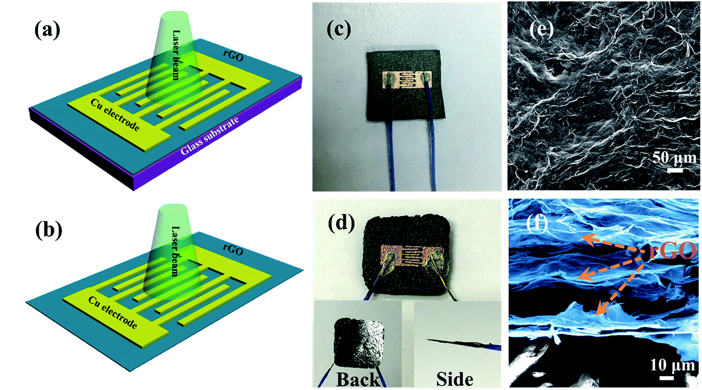 | ||
| Fig. 1 Schematics of (a) supported rGO film device and (b) substrate-free rGO film device. (c) Photograph of supported rGO film device. (d) Photograph of substrate-free rGO film device. (e) Surface view SEM image of rGO film. (f) Cross-section view SEM image of rGO film. | ||
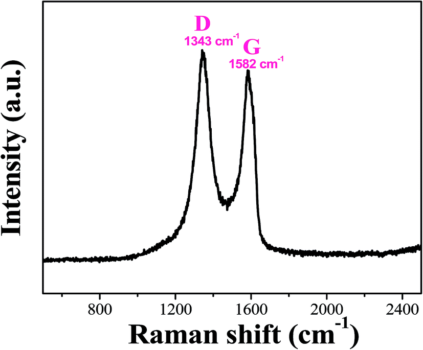 | ||
| Fig. 2 Representative Raman spectrum of rGO film. | ||
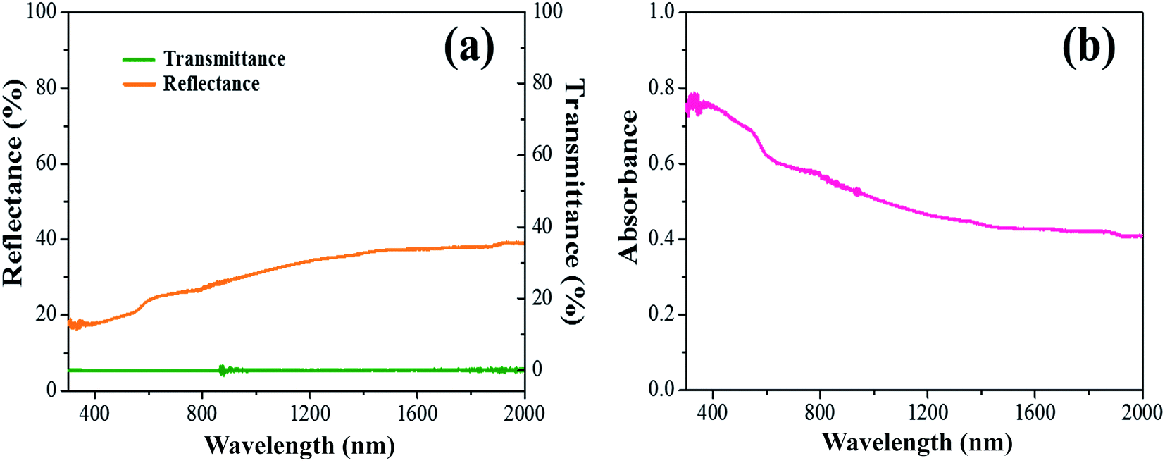 | ||
| Fig. 3 (a) Reflectance (orange line) and transmittance (green line) spectra of rGO film. (b) UV-vis absorbance spectrum of rGO film. | ||
In order to evaluate the performance of supported and substrate-free rGO film photodetectors, photoresponse measurements were carried out under light illumination as schematically illustrated in Fig. 1a and b. The current–voltage (I–V) characteristics in the dark and under illumination (532 nm, 0.28 W cm−2) are shown in Fig. S3 and S4.† The current vs. voltage bias lines demonstrate that the supported and substrate-free devices are highly sensitive. It is also worth noting that compared to the supported device, the substrate-free device exhibits much higher sensitivity.
The thickness of rGO film plays an important role in controlling the device performance. To evaluate the influence of rGO film thickness on device performance, we first compared supported devices with varied rGO film thicknesses, from 43.4 to 121.9 μm, as depicted in Fig. 4a. The photocurrent and responsivity were calculated and are summarized in Fig. 4b. Similar to photocurrent, responsivity initially increases with film thickness until it peaks at 62.5 μm and then drops continuously. Under a 532 nm light illumination with power density of 0.28 W cm−2, the device with 62.5 μm rGO film generated a 0.23 mA photocurrent and 65.3 mA W−1 responsivity. This indicates the strong thickness dependence of photocurrent and responsivity for the supported rGO film devices. High performance of supported rGO film device can be obtained by optimizing the thickness of rGO film.
 | ||
| Fig. 4 Photoresponse of supported rGO film devices. (a) Photocurrent in one period of modulation for supported devices with varied rGO film thicknesses. (b) Plots of photocurrent and responsivity versus thickness of supported rGO film. The power density was kept at 0.28 W cm−2 and the light wavelength was 532 nm. | ||
To examine the role of substrate on the photoresponse of rGO film devices, we measured the responsivities of supported and substrate-free rGO film devices at a bias voltage of 1 V under 0.28 W cm−2 532 nm visible-light illumination. To avoid any influence of intrinsic quality of rGO film, the comparison of photoresponse was carried out on the same device before and after substrate removal. The time-traced photocurrent of rGO film devices with and without substrate are shown in Fig. 5a. Reproducible photocurrents were observed by switching on and off the light illumination both for the supported and substrate-free rGO film devices. The substrate removal led to a remarkable increase in photoresponse and introduced a six-fold photocurrent compared to that of supported device, corresponding to a responsivity of 428 mA W−1 which is ∼10–1000 times higher than those of graphene and other rGO devices (Table 1).
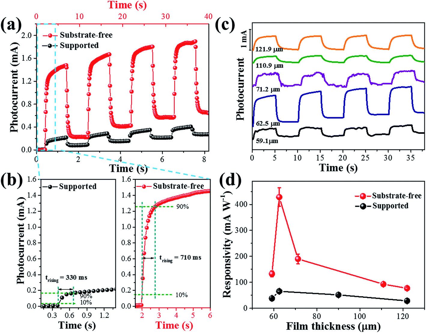 | ||
| Fig. 5 Photoresponse of substrate-free rGO film device under 532 nm light illumination with a light power density of 0.28 W cm−2. (a) Time-traced photocurrent of supported and substrate-free devices with 62.5 μm thick rGO film. (b) The response time at the rise edge for supported and substrate-free devices with 62.5 μm thick rGO film. (c) Photoresponse of substrate-free devices with varied rGO film thicknesses. (d) The plots of responsivity versus thickness of supported and substrate-free devices. Data points are based on the mean value of seven different photoresponse periods. | ||
| Active material | Synthesis method | Bias voltage (V) | Spectral range (nm) | Responsivity (mA W−1) | Rise time (s) | Ref. |
|---|---|---|---|---|---|---|
| a Obtained by seven different photoresponse periods with the corresponding experiments. | ||||||
| Monolayer graphene | Mechanical exfoliation | 532 | 10 | 23 | ||
| Monolayer graphene | CVD | 1 | 532 | 12 | 24 | |
| Twisted bilayer graphene | CVD | 532 | 1 | 5 | ||
| rGO | Chemical reduction | 2 | 1550 | 4 | 2 + 26 | 25 |
| rGO | Chemical reduction | 1 | 360 | 120 | 1800 | 26 |
| rGO film | Chemical reduction | 1 | 850 | 0.0043 | 70 | 27 |
| Thick rGO film (thickness ∼ 60–80 μm) | Chemical reduction | 0 | 633 | 0.27 | 42.5 | 28 |
| Few-layer rGO | Thermal reduction of exfoliated GO | 16 | 895 | 700 (49.3 mA W−1 V−1) | 2 + 20 | 29 |
| Partially suspended graphene | Mechanical exfoliation | 10 | 476 | 2.7 | 17 | |
| Fully suspended graphene | CVD | 532 | ∼0.4 | 18 | ||
| rGO film | Chemical reduction | 1 | 375 | 330 | 0.61a | This work |
| 532 | 428 | 0.78a | This work | |||
| 1064 | 96 | 0.99a | This work | |||
Quantitatively, the photocurrent is directly proportional to photogenerated carriers, which are generated mainly from the photoelectric effect (PE) and/or PTE contribution.30,31 For the PTE effect, the photogenerated carriers are further generated by contributions from photoexcited hot carriers.18 Substrate removal of graphene materials largely reduces the undesirable energy loss of photoexcited hot carriers from surface phonons of the substrate.17,32 Substrate surface polar phonons that are present in common substrates such as SiO2 can provide additional electron energy decay channels.17 All of these enhance the contribution of the PTE effect in the photoresponse of substrate-free rGO film device. Previous studies reveal that the response time of graphene devices based on the PTE effect is much slower than that dominated by the PE effect.18,33 Compared to the PE conversion process, the electron dynamics in PTE after photoexcitation undergoes a relatively flexural process, firstly electron heating through carrier–carrier scattering, and then electron cooling by thermal equilibration with lattice.34 In this work, the photoresponse rise time (trising, 10–90%) of the substrate-free rGO film device is approximately 710 ms, which is much slower than that (ca. 330 ms) of the device with substrate (Fig. 5b). Thus compared with the device with substrate, the PTE effect should play much more important role in the substrate-free rGO film device.
The photoresponse of graphene-based photodetectors have many mechanisms, such as bolometric effect, PE effect, PTE effect and photovoltaic effect, relating to the device design and the active materials. The bolometric effect also originates from thermal, but it is associated with the change in transport conductance of the active material when heated by the incident radiation.35 The PE effect with high response speed has been shown to be dominant in samples with closely spaced metal electrodes and suspended graphene,18 while the slow PTE effect governs the photoresponse in the graphene p–n junctions and partially suspended graphene.36–38 However, as a substrate-free device, the PE effect did not play the main role in our devices.18 This is attributed to the unique features of used rGO film. First, the linearity of I–V characteristics (Fig. S4†) confirms that no p–n junctions exist in the substrate-free rGO film devices, different from previously reported suspended photodetectors based on monolayer or multilayer graphene.18 Second, the high light–matter interaction (∼70% of absorption) of rGO film contributes a large number of photoexcited hot carriers which can lead to pronounced PTE effect. In addition, the puff pastry-like architecture and plentiful interspace in the rGO film (see Fig. 1f) would hamper heat dissipation, and therefore promise relatively pronounced PTE effect and high photoelectric conversion efficiency.
External quantum efficiency (EQE), defined as the number of electrons detected per incident photon, is a crucial factor that determines the photoelectric conversion efficiency and performance of a photodetector.39 According to our calculation using the customary equation as shown in ESI,† the EQE of this substrate-free device with a 62.5 μm thick rGO film is ∼100%, higher than that of many graphene and graphene derivatives.25,39,40 In comparison, the EQE of supported device with the identical rGO film was estimated to be only 15%, much less than that of substrate-free device. This further demonstrates that substrate removal can greatly improve the photoelectric conversion efficiency of rGO film devices.
Similar to the supported rGO film photodetectors and other two-dimensional material photodetectors.41,42 The photoresponse of substrate-free rGO film device strongly depends on the thickness of rGO film, as shown in Fig. 5c and d. We noted that the photoresponse of substrate-free rGO film devices also follow a mountain-type trend, similar to what found for the supported devices in Fig. 4b. Of the samples tested, the substrate-free device with 62.5 μm thick rGO film gives the maximum responsivity of 428 mA W−1. Specifically, these substrate-free rGO film devices achieved responsivities of 133 mA W−1 (59.1 μm), 190 mA W−1 (71.2 μm), 92 mA W−1 (110.9 μm), and 77 mA W−1 (121.9 μm), respectively, all of which climb above that of the ‘peak’ value observed for the supported rGO film devices. For such devices of rGO film with puff pastry-like structure and interdigital electrodes on top of rGO film, very thick rGO film leads to recombination of more photogenerated electrons before they reach the electrodes,43 while thinner rGO film suffers from lower light adsorption. Overall, the optimal thickness of rGO film whether for the supported or support-free devices is 62.5 μm.
Graphene materials have a broadband photoresponse from the UV to IR range.44 For more insight into the broadband photoresponse enhancement behavior of substrate removal, we evaluated the photocurrent switching behaviors of supported and substrate-free rGO film devices under UV and NIR light illumination at 1 V bias, as shown in Fig. 6a and b. For both devices, a strong photoresponse with good stability and reversibility was recorded under UV and NIR light, demonstrating a broadband photodetection characteristic of both rGO film devices. From the supported to substrate-free device, the photocurrent increases remarkably. The responsivity of the supported device was calculated to be 53 mA W−1 at 375 nm and 29 mA W−1 at 1064 nm, and increased to 330 mA W−1 and 96 mA W−1, respectively after removing the substrate (Fig. S5†). This result indicates that the substrate removal can greatly enhance the photoresponse of rGO film photodetector to UV and NIR light. Furthermore, as the photoresponse behavior toward 532 nm light (Fig. 5a and b), the photodetector after removing the substrate also displays a relatively slow response speed toward no matter 375 nm or 1064 nm light (Fig. S6 and S7†). Even so, it is noteworthy that the response times demonstrated here are much faster than most of the previous reports on graphene photodetectors, as presented in Table 1.
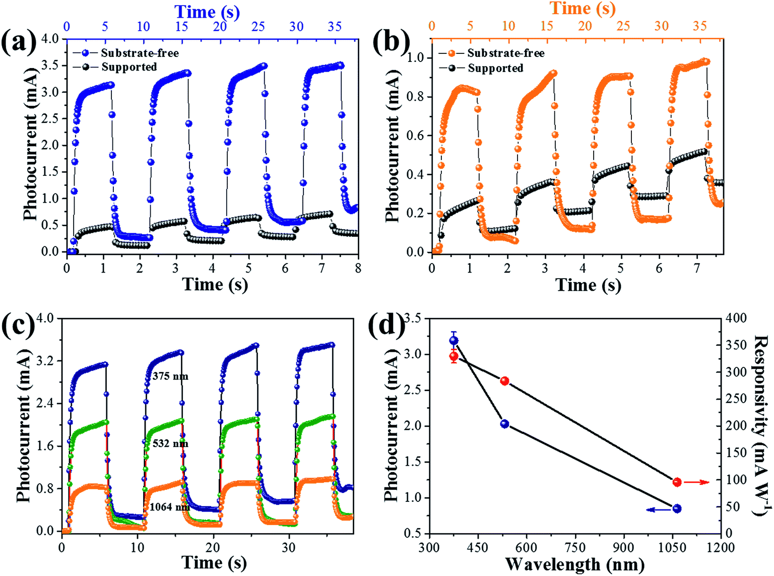 | ||
| Fig. 6 Photoresponse of the devices with 62.5 μm thick rGO film under irradiation at varied wavelengths of incident light. (a and b) Photocurrent switching performance of supported and substrate-free devices under illumination of identical light intensity (∼0.6 W cm−2) at 375 nm and 1064 nm, respectively. (c) Photocurrent switching behaviors of substrate-free rGO film device under UV, visible and NIR light illuminations of ∼0.6 W cm−2. (d) The plots of photocurrent and responsivity versus wavelength, corresponding to the measurements as shown in (c). Data points are based on the mean value of seven different photoresponse periods. | ||
Fig. 6c shows the representative photocurrent switching behaviors of substrate-free rGO film devices under UV (375 nm), visible (532 nm) and NIR (1064 nm) light irradiation of the identical light intensity. It further suggests that the substrate-free rGO film device displays strong and fast photoresponse toward UV-NIR light, indicating a broadband detection ability. The magnitude of photocurrent and responsivity of substrate-free devices under different light wavelengths are illustrated in Fig. 6d. The photocurrent and responsivity decrease with increase of light wavelength. This trend arises most likely from lowered light–matter interaction and lower photon energy at longer wavelengths (Fig. 3b), thus resulting in a lowered efficiency of photogenerated carriers. High responsivity of 330, 284 and 96 mA W−1 were obtained for 375, 532 and 1064 nm wavelengths, respectively. These responsivities are also higher than most of those previously reported using graphene only as active material, over the UV-IR region, see Table 1. According to the equation of EQE (see ESI†), the value of EQE for the substrate-free rGO device with 62.5 μm thick rGO film was calculated to be 110% for 375 nm light, 66% for 532 nm light and 11% for 1064 nm light, respectively, indicating EQE decreases with increase of light wavelength. In addition, we have also analyzed the photoresponse of substrate-free rGO film device at different light power densities (Fig. 7). The photocurrent varies from 1.5 to 9.8 mA, and holds a fine linear relationship with light power density by a fitting curve (Fig. 7b, R2 = 0.998), benefiting calibrations for practical applications.
 | ||
| Fig. 7 (a) Photoresponse of the substrate-free device with 62.5 μm thick rGO film under 532 nm illumination of varied power densities from 0.28 to 3.38 W cm−2. (b) The plot of photocurrent versus power density, corresponding to the measurements in (a). | ||
In addition, it is noted that after turning off irradiation, the rGO film device exhibited a fast current relaxation, but the photocurrent did not restore to its initial value of 0 mA and a very small residual dark current (the photocurrent in the dark in photocurrent versus time curves) remained whether in supported or substrate-free rGO film devices (Fig. 4a, 5a, 6a and b). This can be explained by the photothermal reduction of rGO by light irradiation with relatively high power density.45 The photoinduced enhancement in the reduction level of rGO film would result in an increase in electrical conductivity, thus leading to a decrease in device resistance. In fact, similar observations had been reported in an earlier work where dark current increased in rGO devices.46 These rGO materials were usually fabricated by chemical reduction. The reduction was often below desired levels, leaving many residual oxygen. When they were irradiated by a laser light with high power, further reduction could occur spontaneously. Based on such characteristics, a laser scribing technology has been recently developed to reduce graphene oxide material.47,48 It is worthwhile to emphasize that the substrate plays an important role in the proposed photothermal reduction of rGO film during laser irradiation. As indicated in Fig. 5a and 6a, the residual dark current in substrate-free device is larger than that in the device without substrate after UV or visible light irradiation. This observation could be attributed to the effect of the substrate on the heat dissipation. The glass substrate is an efficient “cooling pad” of the heat induced by light irradiation, and substrate removal greatly reduces the heat loss. The relatively increased photoinduced heat in the substrate-free device leads to a higher reduction level of rGO film and a higher electrical conductivity. The exceptional observation in the case of under IR irradiation (Fig. 6b) may be related to the order of actual measurements. In fact, the photodetection tests under IR irradiation were carried out following the tests under UV and visible light irradiation. After the UV and visible light irradiation, the rGO film in the substrate-free device was reduced so highly that the later IR irradiation just triggered a slight reduction of rGO film. In contrast, the rGO film in the device without substrate was not reduced to a great degree under UV and visible light because of the “cooling pad” effect of substrate. When the light source used for irradiation is IR light, the rGO film might be more significantly reduced, and displayed a higher residual dark current as compared to the substrate-free device.
4. Conclusions
In summary, for the first time we have doubtlessly demonstrated that substrate removal can lead to a broadband enhanced photoresponse of rGO film photodetectors. The substrate-free photodetector with an optimal rGO film thickness possesses a markedly enhanced responsivity of 428 mA W−1 under ambient conditions and a high EQE of 100%, all of which are over six times higher than that of the corresponding rGO film device with substrate. The substrate removal and unique puff pastry-like architecture of rGO thick film largely prevent heat dissipation and increase the PTE effect that can contribute to photocurrent. The substrate removal may also avoid the cooling of photoexcited carriers from substrate surface polar phonons. Furthermore, dramatically high light absorption of rGO thick film also contributes to the photoresponse enhancement. We believe that this proof-of-concept could be universally applied to various rGO-based systems for optoelectronic applications, and provides an alternative route to improve the performance of rGO-based optoelectronic devices.Conflicts of interest
There are no conflicts to declare.Acknowledgements
This work was supported by the Science and Technology Commission of Beijing Municipality (Z151100003315018), the National Key Research and Development Program of China (2017YFA0207102), the National Natural Science Foundation of China (21571182, 21271177), and Technical Institute of Physics and Chemistry, Chinese Academy of Sciences.References
- J. Li, L. Niu, Z. Zheng and F. Yan, Adv. Mater., 2014, 26, 5239–5273 CrossRef CAS PubMed.
- N. G. Kalugin, L. Jing, E. S. Morell, G. C. Dyer, L. Wickey, M. Ovezmyradov, A. D. Grine, M. C. Wanke, E. A. Shaner, C. N. Lau, L. E. F. Foa Torres, M. V. Fistul and K. B. Efetov, 2D Materials, 2016, 4, 015002 CrossRef.
- A. Urich, K. Unterrainer and T. Mueller, Nano Lett., 2011, 11, 2804–2808 CrossRef CAS PubMed.
- H. Tetsuka, A. Nagoya and S. I. Tamura, Nanoscale, 2016, 8, 19677–19683 RSC.
- J. Yin, H. Wang, H. Peng, Z. Tan, L. Liao, L. Lin, X. Sun, A. L. Koh, Y. Chen, H. Peng and Z. Liu, Nat. Commun., 2016, 7, 10699 CrossRef CAS PubMed.
- R. Lu, J. Liu, H. Luo, V. Chikan and J. Z. Wu, Sci. Rep., 2016, 6, 19161 CrossRef CAS PubMed.
- S. Liu, Q. Liao, S. Lu, Z. Zhang, G. Zhang and Y. Zhang, Adv. Funct. Mater., 2016, 26, 1347–1353 CrossRef CAS.
- L. Lin, X. Xu, J. Yin, J. Sun, Z. Tan, A. L. Koh, H. Wang, H. Peng, Y. Chen and Z. Liu, Nano Lett., 2016, 16, 4094–4101 CrossRef CAS PubMed.
- L.-B. Luo, H. Hu, X.-H. Wang, R. Lu, Y.-F. Zou, Y.-Q. Yu and F.-X. Liang, J. Mater. Chem. C, 2015, 3, 4723–4728 RSC.
- G. Konstantatos, M. Badioli, L. Gaudreau, J. Osmond, M. Bernechea, F. P. Garcia de Arquer, F. Gatti and F. H. Koppens, Nat. Nanotechnol., 2012, 7, 363–368 CrossRef CAS PubMed.
- X. Yu, Z. Dong, J. K. W. Yang and Q. J. Wang, Optica, 2016, 3, 979 Search PubMed.
- P. K. Herring, A. L. Hsu, N. M. Gabor, Y. C. Shin, J. Kong, T. Palacios and P. Jarillo-Herrero, Nano Lett., 2014, 14, 901–907 CrossRef CAS PubMed.
- F. H. Koppens, T. Mueller, P. Avouris, A. C. Ferrari, M. S. Vitiello and M. Polini, Nat. Nanotechnol., 2014, 9, 780–793 CrossRef CAS PubMed.
- Z. Sun, Z. Liu, J. Li, G. A. Tai, S. P. Lau and F. Yan, Adv. Mater., 2012, 24, 5878–5883 CrossRef CAS PubMed.
- M. Gong, Q. Liu, B. Cook, B. Kattel, T. Wang, W. L. Chan, D. Ewing, M. Casper, A. Stramel and J. Z. Wu, ACS Nano, 2017, 11, 4114–4123 CrossRef CAS PubMed.
- Q. Zhang, J. Jie, S. Diao, Z. Shao, Q. Zhang, L. Wang, W. Deng, W. Hu, H. Xia, X. Yuan and S. Lee, ACS Nano, 2015, 9, 1561–1570 CrossRef CAS PubMed.
- M. Freitag, T. Low and P. Avouris, Nano Lett., 2013, 13, 1644–1648 CrossRef CAS PubMed.
- V. Patil, A. Capone, S. Strauf and E. H. Yang, Sci. Rep., 2013, 3, 2791 CrossRef PubMed.
- X. Li, J. Wu, N. Mao, J. Zhang, Z. Lei, Z. Liu and H. Xu, Carbon, 2015, 92, 126–132 CrossRef CAS.
- H. Yang, Y. Cao, J. He, Y. Zhang, B. Jin, J.-L. Sun, Y. Wang and Z. Zhao, Carbon, 2017, 115, 561–570 CrossRef CAS.
- L. Lu, H. Tian, J. He and Q. Yang, J. Phys. Chem. C, 2016, 120, 23660–23668 CAS.
- S. Ishida, Y. Anno, M. Takeuchi, M. Matsuoka, K. Takei, T. Arie and S. Akita, Sci. Rep., 2015, 5, 15491 CrossRef CAS PubMed.
- J. Park, Nano Lett., 2009, 9, 1742–1746 CrossRef CAS PubMed.
- F. Xing, W. Xin, W.-S. Jiang, Z.-B. Liu and J.-G. Tian, Appl. Phys. Lett., 2015, 107, 163110 CrossRef.
- B. Chitara, L. S. Panchakarla, S. B. Krupanidhi and C. N. Rao, Adv. Mater., 2011, 23, 5419–5424 CrossRef CAS PubMed.
- B. Chitara, S. B. Krupanidhi and C. N. R. Rao, Appl. Phys. Lett., 2011, 99, 113114 CrossRef.
- Y. Cao, J. Zhu, J. Xu and J. He, Carbon, 2014, 77, 1111–1122 CrossRef CAS.
- I. K. Moon, B. Ki, S. Yoon and J. Oh, Sci. Rep., 2016, 6, 33525 CrossRef CAS PubMed.
- H. Chang, Z. Sun, M. Saito, Q. Yuan, H. Zhang, J. Li, Z. Wang, T. Fujita, F. Ding, Z. Zheng, F. Yan, H. Wu, M. Chen and Y. Ikuhara, ACS Nano, 2013, 7, 6310–6320 CrossRef CAS PubMed.
- T. J. Echtermeyer, P. S. Nene, M. Trushin, R. V. Gorbachev, A. L. Eiden, S. Milana, Z. Sun, J. Schliemann, E. Lidorikis, K. S. Novoselov and A. C. Ferrari, Nano Lett., 2014, 14, 3733–3742 CrossRef CAS PubMed.
- B. D. Boruah, A. Mukherjee and A. Misra, Nanotechnology, 2016, 27, 095205 CrossRef PubMed.
- X. Yu, Z. Dong, Y. Liu, T. Liu, J. Tao, Y. Zeng, J. K. Yang and Q. J. Wang, Nanoscale, 2016, 8, 327–332 RSC.
- L. Prechtel, L. Song, D. Schuh, P. Ajayan, W. Wegscheider and A. W. Holleitner, Nat. Commun., 2012, 3, 646 Search PubMed.
- K. J. Tielrooij, L. Piatkowski, M. Massicotte, A. Woessner, Q. Ma, Y. Lee, K. S. Myhro, C. N. Lau, P. Jarillo-Herrero, N. F. van Hulst and F. H. Koppens, Nat. Nanotechnol., 2015, 10, 437–443 CrossRef CAS PubMed.
- X. Deng, Y. Wang, Z. Zhao, Z. Chen and J.-L. Sun, J. Phys. D: Appl. Phys., 2016, 49, 425101 CrossRef.
- N. M. Gabor, J. C. Song, Q. Ma, N. L. Nair, T. Taychatanapat, K. Watanabe, T. Taniguchi, L. S. Levitov and P. Jarillo-Herrero, Science, 2011, 334, 648–652 CrossRef CAS PubMed.
- I. J. Luxmoore, P. Q. Liu, P. Li, J. Faist and G. R. Nash, ACS Photonics, 2016, 3, 936–941 CrossRef CAS.
- X. He, X. Wang, S. Nanot, K. Cong, Q. Jiang, A. A. Kane, J. E. M. Goldsmith, R. H. Hauge, F. Leonard and J. Kono, ACS Nano, 2013, 7, 7271–7277 CrossRef CAS PubMed.
- Y. Liu, F. Wang, X. Wang, X. Wang, E. Flahaut, X. Liu, Y. Li, X. Wang, Y. Xu, Y. Shi and R. Zhang, Nat. Commun., 2015, 6, 8589 CrossRef CAS PubMed.
- P. Gowda, D. R. Mohapatra and A. Misra, ACS Appl. Mater. Interfaces, 2014, 6, 16763–16768 CAS.
- R. Sun, Y. Zhang, K. Li, C. Hui, K. He, X. Ma and F. Liu, Appl. Phys. Lett., 2013, 103, 013106 CrossRef.
- J. Pak, J. Jang, K. Cho, T. Y. Kim, J. K. Kim, Y. Song, W. K. Hong, M. Min, H. Lee and T. Lee, Nanoscale, 2015, 7, 18780–18788 RSC.
- D. D. Tune, B. S. Flavel, R. Krupke and J. G. Shapter, Adv. Energy Mater., 2012, 2, 1043–1055 CrossRef CAS.
- H. Liu, Q. Sun, J. Xing, Z. Zheng, Z. Zhang, Z. Lu and K. Zhao, ACS Appl. Mater. Interfaces, 2015, 7, 6645–6651 CAS.
- Y. Zhao, Q. Han, Z. Cheng, L. Jiang and L. Qu, Nano Today, 2017, 12, 14–30 CrossRef CAS.
- D. Alsaedi, M. Irannejad, K. H. Ibrahim, A. Almutairi, O. Ramahi and M. Yavuz, J. Mater. Chem. C, 2017, 5, 882–888 RSC.
- X. Wang, H. Tian, M. A. Mohammad, C. Li, C. Wu, Y. Yang and T. L. Ren, Nat. Commun., 2015, 6, 7767 CrossRef CAS PubMed.
- H. Tian, Y. Yang, D. Xie, Y. L. Cui, W. T. Mi, Y. Zhang and T. L. Ren, Sci. Rep., 2014, 4, 3598 CrossRef PubMed.
Footnote |
| † Electronic supplementary information (ESI) available. See DOI: 10.1039/c7ra09826j |
| This journal is © The Royal Society of Chemistry 2017 |