
 Open Access Article
 This Open Access Article is licensed under a Creative Commons Attribution-Non Commercial 3.0 Unported Licence
Controlled growth of aligned GaN nanostructures: from nanowires and needles to micro-rods on a single substrate†
Danna Zhao ,
Hui Huang*,
Rui Lv,
Shunji Chen,
Qiyilan Guang,
Yang Zong,
Zhe Liu and
Xiqing Li
,
Hui Huang*,
Rui Lv,
Shunji Chen,
Qiyilan Guang,
Yang Zong,
Zhe Liu and
Xiqing Li
Department of Electronic Science and Technology, Faculty of Electronic Information and Electrical Engineering, Dalian University of Technology, Dalian 116024, China. E-mail: huihuang@dlut.edu.cn
First published on 1st November 2017
Abstract
Simultaneous growth of different kinds of aligned GaN nanostructures (i.e., nanowires, needles, pyramids and micro-rods) on a single substrate was firstly realized at a low temperature of 790 °C by naturally changing the III/V ratio across the substrate via a coaxial pipeline configuration. The effects of substrate distance and growth pressure on nanostructure growth were investigated. The morphology variation from nanowires to micros-rods would be explained in terms of Ga species changing from the Ga element to GaN molecule in a hot-wall reactor. This work is helpful for on chip integration of different kinds of nanodevices on unusual substrates of low melting temperature.
1. Introduction
Semiconductor nanostructures, such as nanowires,1–3,12–15,24–29 needles,4–6 pyramids,7,8,16,38 rod/pillars,8,9,16–23 and trumpets,10,11 have wide applications in novel electronic devices. In comparison with the nanowire structure,1–3,12–15,27,29 vertically aligned needle, rod and pyramid structures, which have a nanoscale tip and robust microscale-trunk, can bring advantages in single nano-structure devices4–6 and optical coupling.10,11Currently, metal–organic chemical vapor deposition (MOCVD) is one of the most popular techniques for commercialized GaN epitaxy. For MOCVD growth of GaN nanostructures, there has two main methods, i.e., vapor–liquid(solid)–solid growth with metal catalyst (VLS)1,2,12,13,24–27,29 and catalyst-free anisotropic-growth on patterned substrate (i.e., selective area growth (SAG)).7–9,16–23 However, for the nanowires with high aspect ratio (length/diameter > 35), it is difficult to be grown via SAG method7–9,16–18,22,23,39 without the use of high silane flux18,20 or complex pulsed-growth mode.24 While, for the micro-rods of low aspect ratio (i.e., microscale-trunk rods), there is few report that they can be grown via VLS method.1,2,12,13,24–27,29 In other word, neither VLS nor SAG can be satisfactorily used for growth of both nanowires and micro-rods.
Moreover, for different nanostructures, there exists large difference in growth conditions (especially in the growth temperature). Kuykendall et al.2 achieved nanowire arrays via VLS at 780 °C. Tian et al.36 prepared micro-pyramids via SAG at a high temperature about 1080 °C. Bae et al.37 investigated the morphologies of micro-pyramids, and they found that micro-pyramids with smooth sidewalls can only be grown at the temperature higher than 900 °C. Rozhavskaya et al.3 reported the growth of micro-rod arrays under 1040 °C. Thus, growth temperature of these micro-structures prepared via SAG (950–1175 °C)7–9,16–18,22,23 is much higher than that of nanowires prepared via VLS (760–850 °C).1,2,12,13,24–27,29 Thus, it is still a challenge to simultaneous growth of all these nanostructures (including nanowires and micro-rods) under a favorable condition.
In this paper, aligned GaN nanowires, needles, pyramids and micro-rods can be grown simultaneously on a single substrate at a constant temperature of 790 °C, by naturally changing the V/III ratio across the substrate. The growth mechanism, which induces the transformation between these nanostructures, was also discussed.
2. Experiment
Growth of the GaN nanostructures was performed by using a homemade hot-wall MOCVD system, in which the growth parameters can be flexibly tuned. As shown in Fig. 1(a), the substrate distance (defined as the distance between the substrate and the outlet of quartz coaxial pipeline) can be changed. The coaxial pipeline contains an inner-tube (4 mm i.d., 5 mm o.d.) and an outer-tube (7 mm i.d., 8 mm o.d.), which is used for delivering TMGa and NH3 to the substrate, respectively. This coaxial pipeline configuration results in a gradual decrease of the III/V ratio from the center (point 1#) to the edge of the substrate, while the other growth parameters can remain the same across the substrate. Thus, the effect of III/V ratio on nanostructure growth can be found out on a single substrate, by carrying out only a single growth, which can eliminate the run to run variation.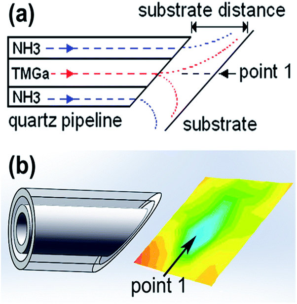 | ||
| Fig. 1 (a) Schematic diagram and (b) gas distributions of the coaxial pipeline. | ||
As listed in Table 1, three samples were grown at an optimized temperature of 790 °C for 15 min. The flow rate of N2/(5%)H2 gas used for carrying TMGa and NH3 precursors was 350 sccm and 150 sccm, respectively. (0001) sapphire wafer coated with a 3 μm (0001) GaN-layer was employed as substrate. (2 nm)Ni/(2 nm)Au catalyst layers were successively deposited on the substrate by magnetron sputtering.
| Sample | TMGa [μmol min−1] | NH3 [mmol min−1] | Pressure [Torr] | Substrate distance [mm] |
|---|---|---|---|---|
| A | 100 | 8 | ||
| B1 | 9 | 1.8 | 100 | 18 |
| B2 | 200 | 18 |
3. Results
Sample A
Fig. 2(a) shows the optical photograph of sample A, which was grown with a substrate distance of 8 mm. With such a short distance, the mixture between TMGa and NH3 precursors was far from homogeneous when they arriving the substrate, so the III/V ratio can change greatly across the substrate. As shown in Fig. 2(a), with moving from the center (point 1#) to the edge (point 5#) of the growth region (indicated by the red circle) on the substrate, the surface color changes from black (1#), yellow (2#, 3#), to light yellow (4#, 5#). The black-disk (around point 1#) is the region, which directly faces the inner-tube of the coaxial pipeline (Fig. 1).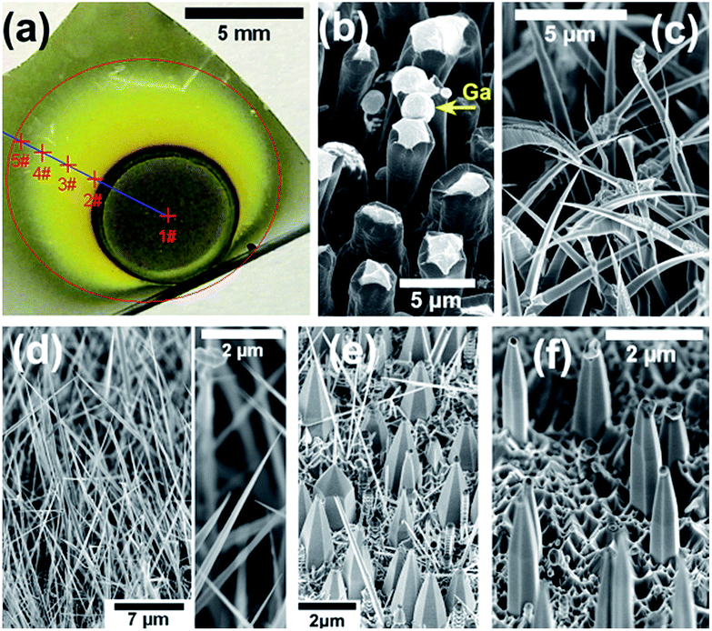 | ||
| Fig. 2 (a) The optical photograph and the SEM images of point (b) 1#, (c) 2#, (d) 3#, (e) 4#, and (f) 5# of sample A. | ||
Fig. 2(b)–(f) show the scanning electron microscopy (SEM) images of the five points (1#–5#) of sample A, respectively. At point 1# (Fig. 2(b)), distorted large rods were observed with white cap (indicated by an arrow), which could be induced by excess supply of Ga species, because of extremely high III/V ratio at the region of the black-disk. At point 2# (Fig. 2(c)), curve needles (base diameter of ∼700 nm and length of ∼20 μm) were observed without excess Ga at the tip. At point 3# (Fig. 2(d)), oriented triangular nanowires with diameter of ∼200 nm and length of ∼20 μm were observed. At point 4# (Fig. 2(e)), vertical hexagonal pyramids with base diameter of ∼1.5 μm and length of ∼4 μm were observed. At point 5# (Fig. 2(f)), vertical hexagonal micro-rods with trunk diameter of ∼0.7 μm and length of ∼3 μm were observed. At the points outside the growth region, nanostructures are very sparse due to lack of Ga species (i.e., extremely low III/V ratio). Thus, by simply decreasing the III/V ratio across the substrate, the nanostructures of needles (2#), nanowires (3#), pyramids (4#), or micro-rods (5#) can be obtained respectively. As shown in the S1–S2 of the ESI,† the growth directions of nanowire and pyramid are [10![[1 with combining macron]](https://www.rsc.org/images/entities/char_0031_0304.gif) 0] and [0001], respectively.
0] and [0001], respectively.
Sample B1
Fig. 3(a) shows the optical photograph of sample B1, which was grown with an increased substrate distance of 18 mm. The increased distance would enhance the mixture of TMGa and NH3 precursors before they arrive the substrate, so more uniform distribution of the nanostructures across the substrate can be obtained. As shown in Fig. 3(a), only yellow-green color was observed, and the color depth decreases slightly from the center (point 1#) to the edge (point 2#) of the growth region.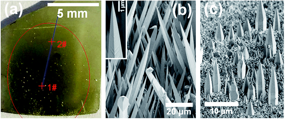 | ||
| Fig. 3 (a) The optical photograph and the SEM images at point (b) 1#, (c) 2# of sample B1. | ||
Fig. 3(b) and (c) shows the SEM images of sample B1. At point 1# (Fig. 3(b)), oriented triangular needles with base diameter of ∼5 μm and length of ∼40 μm were observed. At point 2# (Fig. 3(c)), vertical hexagonal micro-rods with trunk diameter of ∼2.6 μm and length of ∼8 μm were observed. Thus, by decreasing the III/V ratio across the substrate, the nano-structures can change from triangular needles (1#) to hexagonal micro-rods (2#). This trend of morphology transformation is similar with that observed in sample A. As shown in the S3–S4 of the ESI,† the growth directions of needle and micro-rod are [100] and [0001], respectively, which are confirmed by XRD measurement (S6 of the ESI†).
Sample B2
Fig. 4(a) shows the optical photograph of sample B2, which was also grown with a substrate distance of 18 mm. While the growth pressure was increased from 100 Torr to 200 Torr, which would further enhance the mixture of TMGa and NH3. As shown in Fig. 4(a), the surface color is uniform inside the growth region.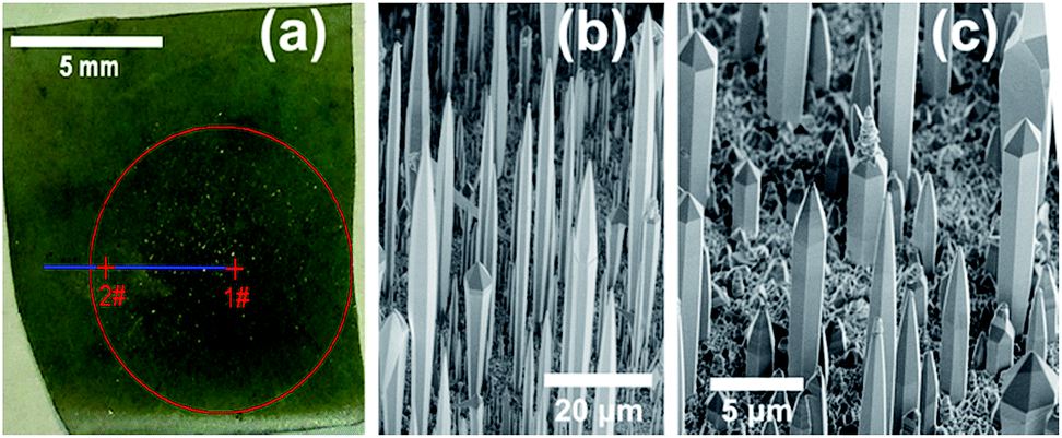 | ||
| Fig. 4 (a) The optical photograph and the SEM images at point (b) 1#, (c) 2# of sample B2. | ||
Fig. 4 shows the SEM images of sample B2, and vertical hexagonal micro-rods with an average trunk diameter of ∼3 μm were observed across the growth region. With moving from the center (point 1#) to the edge (point 2#) of the growth region, the length of micro-rods decreases from ∼40 μm (Fig. 4(b)) to ∼15 μm (Fig. 4(c)). In contrast with sample A and B1, there is no obvious morphology variation across the growth region, due to the enhanced mixture of the precursors via increasing the substrate distance and growth pressure.
4. Discussion
As shown in Fig. 5, NiAu droplet tends to leave the tip of the rod (Fig. 5(a)), otherwise the droplet would initiate a new growth of a branch (Fig. 5(b)), a polycrystalline structure (Fig. 5(c)) or a new rod (Fig. 5(d)) at the tip. According to previous report,7 the flat (0001) top surface will gradually shrink with the expanding of {1102} sidewall facets. When the top surface becomes too small to support the NiAu droplet, the droplet would slide to the sidewall. Thus, except the initial stage of nucleation, the NiAu droplet should be not indispensable during the following growth. Moreover, for the nanowires (Fig. 2(d)) and needles (Fig. 3(b)), there is no droplet observed. It can be concluded that the Ni/Au droplet would function as providing nucleation site rather than catalyst.15,24–26,29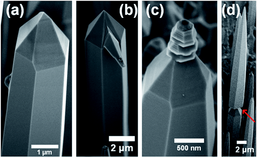 | ||
| Fig. 5 The SEM images of the pillars (a) without NiAu droplet, or with a NiAu droplet at the tip for an additional growth of (b) a branch, (c) a polycrystal, and (d) a new pillar. | ||
As shown in Fig. 4, the GaN hexagonal micro-rods have a similar morphology with previously reported GaN rods,7–9,16 which were grown via SAG. Thus, the growth of micro-rods would have similar mechanism with SAG. In this case, NiAu would promote the pyrolysis of NH3 at a relatively low growth temperature (790 °C), which is helpful for direct growth of nanodevices on unusual substrates of low melting temperature.30–35 While, the growth of nanowires (Fig. 2(d)) would have similar mechanism with VLS, because the nanowires have a high aspect ratio of ∼100, which can not be realized by using normal SAG.7–9,16–18,20,22,23
The underlying growth mechanism in this case would be neither pure VLS1,2,12,13,24–27,29 nor pure SAG,7–9,16–18,22,23 because of the factors: (1) for VLS, metal droplet can normally be observed at the tip of nanowires, but in our case there is no droplet at the tip of nanowires (Fig. 2(d)) or needles (Fig. 3(b)); (2) for SAG, metal catalyst is needless, but in our case the nanostructures can not grow without NiAu (not shown).
The growth mechanism schematic of the nanostructures was shown in Fig. 6. It is clear that the morphology variation from nanowire to micro-rod (Fig. 2) was mainly resulted from the decreasing of III/V ratio across the substrate. The III/V ratio was relatively high at center region, Ga element dominates and results in nanowire growth. When the III/V ratio is gradually decreased and the transport distance of Ga species is increased, the Ga species tends to react with NH3 and form GaN molecules in gas ambient due to the hot-wall reactor. Thus, there is a different growth mechanism, which includes: (1) the Ni/Au would play the role of providing nucleation site rather than catalyst; (2) the hot-wall MOCVD reactor enhances the pre-reaction between TMGa and NH3 in gas ambient, which produces the species of GaN molecule besides the Ga element; (3) the ratio between Ga element and GaN molecule is decided by the transport distance of Ga species; (4) Ga element dominates at center region and results in nanowire growth, while GaN molecule dominates at edge region and results in micro-rod growth. In-depth analysis will be carried out in our future study.
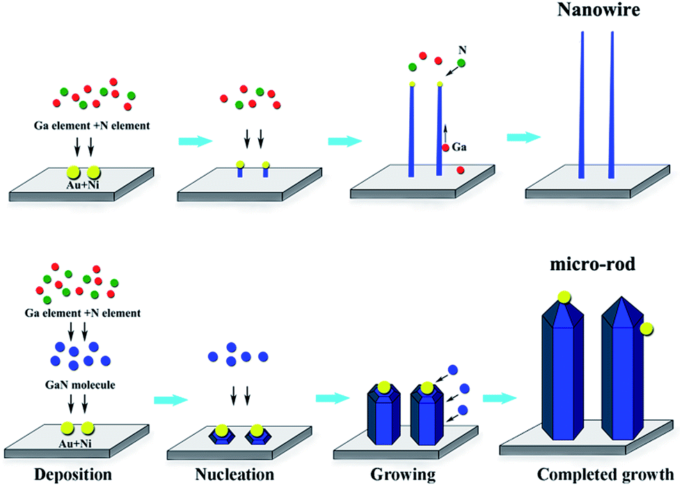 | ||
| Fig. 6 The growth mechanism schematic of nanowires and micro-rods. | ||
Fig. 7(a) shown the diameter distribution of sample A, B1 and B2. For sample A, the diameter is not continuously decreasing with III/V ratio decreasing from the center to the edge of the substrate. While for sample B1 and B2, the diameter was continuously decreasing with III/V ratio decreasing. The different variation trend of nanostructure diameter could be attributed to the difference of growth mechanisms. It can be seen from Fig. 2 that the nanostructure of sample A grown from position 1# to position 3# was nanowire which has similar mechanism with VLS, while from position 4# to 5#, pyramid and micro-rod were observed, which have similar mechanism with SAG. So for the nanostructures grown under the same mechanism, the diameter decreased with decreasing III/V ratio from the center to the edge of the substrate. Fig. 7(b) shown the height distribution of three samples. For sample A, with decreasing III/V ratio, the height is decreasing except for the position 1# where distorted large rods are observed. The short large rods are induced by very high III/V ratio and the lacking of N element for growth. For sample B1 and sample B2 (needles and micro-rods), the height has the same trend of change with localized III/V ration. In a word, both the height and diameter can be controlled by changing III/V ratio.
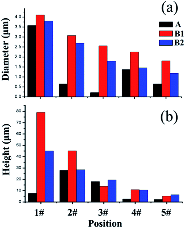 | ||
| Fig. 7 The (a) diameter and (b) height distributions of sample A, B1 and B2 at different positions of the substrate. | ||
5. Conclusions
Different kinds of aligned GaN nanostructures (i.e., nanowires, needles and micro-rods) can be simultaneously grown on a single substrate, by naturally changing the III/V ratio across the substrate. The morphology variation from nanowires to micro-rods would be resulted from that the Ga species arriving at the substrate changes from Ga element to GaN molecule. Growth of these nanostructures on a single substrate at a temperature of 790 °C, which is much lower than that of SAG, is helpful for on chip integration of different kinds of nanodevices on unusual substrates of low melting temperature.Conflicts of interest
There are no conflicts to declare.Acknowledgements
This research was supported by grants from the New Century Excellent Talents in the University of China (NCET-05-0111), the International S&T Cooperation Program of China (No. 2015DFR10970), and the National Natural Science Foundation of China (No. 61774027 and 61376050).References
- F. Qian, Y. Li, S. Gradečak, D. Wang, C. J. Barrelet and C. M. Lieber, Nano Lett., 2004, 4(10), 1975–1979 CrossRef CAS.
- T. R. Kuykendall, M. V. Altoe, D. F. Ogletree and S. Aloni, Nano Lett., 2014, 14, 6767–6773 CrossRef CAS PubMed.
- M. M. Rozhavskaya, W. V. Lundin, E. Y. Lundina, V. Y. Davydov, S. I. Troshkov, A. A. Vasilyev, P. N. Brunkov, A. V. Baklanov, A. F. Tsatsulnikov and V. G. Dubrovskii, J. Appl. Phys., 2015, 117, 024301 CrossRef.
- R. Chen, T. Tran, K. Ng, W. Ko, L. Chuang, F. Sedgwick and C. Hasnain, Nat. Photonics, 2011, 5, 170–175 CrossRef CAS.
- L. Chuang, F. Sedgwick, R. Chen, W. Ko, M. Moewe, K. Ng, T. Tran and C. Hasnain, Nano Lett., 2011, 11, 385–390 CrossRef CAS PubMed.
- L. Chuang, M. Moewe, K. Ng, T. Tran, S. Crankshaw, R. Chen, W. Ko and C. Hasnain, Appl. Phys. Lett., 2011, 98, 123101 CrossRef.
- A. Lundskog, U. Forsberg, P. O. Holtz and E. Janzén, Cryst. Growth Des., 2012, 12, 5491–5496 CAS.
- Y. T. Lin, T. W. Yeh, Y. Nakajima and P. D. Dapkus, Adv. Funct. Mater., 2014, 24, 3162–3171 CrossRef CAS.
- K. Choi, M. Arita and Y. Arakawa, J. Cryst. Growth, 2012, 357, 58–61 CrossRef CAS.
- M. Munsch, N. S. Malik, E. Dupuy, A. Delga, J. Bleuse, J. M. Gérard, J. Claudon, N. Gregersen and J. Mørk, Phys. Rev. Lett., 2013, 110, 177402 CrossRef PubMed.
- P. Stepanov, A. Delga, N. Gregersen, E. Peinke, M. Munsch, J. Teissier, J. Mørk, M. Richard, J. Bleuse, J. M. Gérard and J. Claudon, Appl. Phys. Lett., 2015, 107, 141106 CrossRef.
- X. Zhou, J. Chesin, S. Crawford and S. Gradečak, Nanotechnology, 2012, 23, 285603 CrossRef PubMed.
- Q. Li and G. Wang, Appl. Phys. Lett., 2008, 93, 043119 CrossRef.
- G. Mitta and I. Lahiri, J. Phys. D: Appl. Phys., 2014, 47, 323001 CrossRef.
- T. R. Kuykendall, A. M. Schwartzberg and S. Aloni, Adv. Mater., 2015, 27(38), 5805–5812 CrossRef CAS PubMed.
- B. O. Jung, S. Y. Bae, Y. Kato, M. Imura, D. S. Lee, Y. Honda and H. Amano, CrystEngComm, 2014, 16, 2273–2282 RSC.
- P. M. Coulon, B. Alloing, V. Brändli, P. Vennéguès, M. Leroux and J. Zúñiga-Pérez, Appl. Phys. Express, 2016, 9, 015502 CrossRef.
- J. Hartmann, X. Wang, H. Schuhmann, W. Dziony, L. Caccamo, J. Ledig, M. S. Mohajerani, T. Schimpke, M. Bähr, G. Lilienkamp, W. Daum, M. Seibt, M. Straßburg, H. H. Wehmann and A. Waag, Phys. Status Solidi A, 2015, 212, 2830–2836 CrossRef CAS.
- C. Tessarek, S. Figge, A. Gust, M. Heilmann, C. Dieker, E. Spiecker and S. Christiansen, J. Phys. D: Appl. Phys., 2014, 47, 394008 CrossRef.
- R. Koester, J. S. Hwang, C. Durand, D. L. S. Dang and J. Eymery, Nanotechnology, 2010, 21, 015602 CrossRef CAS PubMed.
- X. J. Chen, B. Gayral, D. Sam-Giao, C. Bougerol, C. Durand and J. Eymery, Appl. Phys. Lett., 2011, 99, 251910 CrossRef.
- C. G. Tu, C. Y. Su, C. H. Liao, C. Hsieh, Y. F. Yao, H. T. Chen, C. H. Lin, C. M. Weng, Y. W. Kiang and C. C. Yang, Nanotechnology, 2016, 27, 025303 CrossRef PubMed.
- B. O. Juna, S. Y. Bae, S. Y. Kim, S. Lee, J. Y. Lee, D. S. Lee, Y. Kato, Y. Honda and H. Amano, Nano Energy, 2015, 11, 294–303 CrossRef.
- B. Alloing and J. Zúñiga-Pérez, Mater. Sci. Semicond. Process., 2016, 55, 51–58 CrossRef CAS.
- V. G. Dubrovskii, N. V. Sibirev, J. C. Harmand and F. Glas, Phys. Rev. B: Condens. Matter Mater. Phys., 2008, 78, 235301 CrossRef.
- J. Johansson, C. P. T. Svensson, T. Mårtensson, L. Samuelson and W. Seifert, J. Phys. Chem. B, 2005, 109, 13567–13571 CrossRef CAS PubMed.
- T. Kuykendall, P. Pauzauskie, S. Lee, Y. Zhang, J. Goldberger and P. Yang, Nano Lett., 2003, 3(8), 1063–1066 CrossRef CAS.
- H. Li, A. H. Chin and M. K. Sunkara, Adv. Mater., 2006, 18, 216–220 CrossRef CAS.
- W. C. Hou, T. H. Wu, W. C. Tang and F. C. Hong, Nanoscale Res. Lett., 2012, 7, 373 CrossRef PubMed.
- Y. Sato, A. Fujiwara, S. Ishizaki, S. Nakane and Y. Murakami, Phys. Status Solidi C, 2017, 14, 1600151 Search PubMed.
- S. Y. Bae, J. W. Min, H. Y. Hwang, K. Lekhal, H. J. Lee, Y. D. Jho, D. S. Lee, Y. T. Lee, N. Ikarashi, Y. Honda and H. Amano, Sci. Rep., 2017, 7, 45345 CrossRef CAS PubMed.
- T. Itoh, A. Kobayashi, K. Ueno, J. Ohta and H. Fujioka, Sci. Rep., 2016, 6, 29500 CrossRef CAS PubMed.
- J. H. Choi, A. Zoulkarneev, S. I. Kim, C. W. Baik, M. H. Yang, S. S. Park, H. Suh, U. J. Kim, H. B. Son, J. S. Lee, M. Kim, J. M. Kim and K. Kim, Nat. Photonics, 2011, 5, 763–769 CrossRef CAS.
- J. H. Choi, J. Kim, H. Yoo, J. Liu, S. Kim, C. W. Baik, C. Cho, J. G. Kang, M. Kim, P. V. Braun, S. Hwang and T. S. Jung, Adv. Opt. Mater., 2016, 4, 505–521 CrossRef CAS.
- K. Chen, R. Kapadia, A. Harker, S. Desai, J. S. Kang, S. Chuang, M. Tosun, C. M. Sutter-Fella, M. Tsang, Y. Zeng, D. Kiriya, J. Hazra, S. R. Madhvapathy, M. Hettick, Y. Z. Chen, J. Mastandrea, M. Amani, S. Cabrini, Y. L. Chueh, J. W. Ager III, D. C. Chrzan and A. Javey, Nat. Commun., 2016, 7, 10502 CrossRef CAS PubMed.
- Z. Tian, Y. Li, X. Su, L. Feng, S. Wang, M. Zhang, W. Ding, Q. Li, Y. Zhang, M. Guo, F. Yun and S. W. Ricky Lee, Appl. Phys. Express, 2017, 10, 092101 CrossRef.
- S. Y. Bae, K. Lekhal, H. J. Lee, T. Mitsunari, J. W. Min, D. S. Lee, M. Kushimoto, Y. Honda and H. Amano, J. Cryst. Growth, 2017, 468, 110 CrossRef CAS.
- J. Chen, P. Huang, X. Han, Z. Pan, C. Zhong, J. Liang, Z. Wu, Y. Liu and B. Zhang, Chin. Phys. B, 2017, 26, 068101 CrossRef.
- M. Nami, R. F. Eller, S. Okur, A. K. Rishinaramangalam, S. Liu, I. Brener and D. F. Feezell, Nanotechnology, 2017, 28, 025202 CrossRef PubMed.
Footnote |
| † Electronic supplementary information (ESI) available: S1–S2 Transmission electron microscopy (TEM) analyses of nanowire and pyramid from sample A. S3–S4 The TEM analyses of the triangular needle and hexagonal rod from sample B1. S5 The TEM analyses of the hexagonal rod from sample B2. S6 The X-ray diffraction spectra of sample B1, sample B2 and substrate. S7 The photoluminescence (PL) spectra of nanowires, needles and micro-rods. See DOI: 10.1039/c7ra09813h |
| This journal is © The Royal Society of Chemistry 2017 |