
 Open Access Article
 This Open Access Article is licensed under a
 Creative Commons Attribution 3.0 Unported Licence
Multilevel data storage memory based on polycrystalline SrTiO3 ultrathin film
Pengfei Hou *,
Zhanzhan Gao and
Kaikai Ni
*,
Zhanzhan Gao and
Kaikai Ni
School of Materials Science and Engineering, Xiangtan University, Xiangtan 411105, Hunan, China. E-mail: pfhou@xtu.edu.cn; 2008.houpengfei@xtu.edu.cn; Fax: +86-731-58298119; Tel: +86-731-58293030
First published on 25th October 2017
Abstract
Resistive switching random access memory (RRAM) has recently inspired scientific and commercial interest due to its high operation speed, high scalability, and multilevel data storage potential. However, the switch ratio, energy consumption and retention are still not satisfactory in the devices based on perovskite oxides. Herein, we have prepared polycrystalline SrTiO3 ultrathin film based multilevel data storage memories with different top electrodes and investigated the different performances of these devices. The multilevel data storage of the device with an Ag top electrode is achieved by controlling the shape of the Ag filament using voltage pulses, and the switching ratio can be as high as 107%. The multilevel data storage of device with a Pt top electrode, for comparison, is achieved by controlling the distance of oxygen vacancies migration using voltage sweeping, and the switching ratio is about 106%. The devices, all with good retention, suggest a new opportunity for polycrystalline SrTiO3 ultrathin film based resistive switching devices as high storage density, low-energy and cheaper nonvolatile memories.
1. Introduction
Resistive switching memory has recently inspired scientific and commercial interest due to its high operation speed, high scalability, and multibit-storage potential.1–4 And a variety of new materials and concepts have been explored for resistive switching based memories.3,5–9 Reading of the resistance states is nondestructive, and the memory devices can be operated without transistors in every cell, thus making a cross-bar structure feasible.10,11 People have found that oxygen vacancies and metal ions are very important in the resistive switching devices.12–16 And how oxygen vacancies and metal ions work in the devices are understandable. Further many materials can not only be used in the device based on an oxygen vacancy filament but also the device with a metal ion filament, the only difference between the devices may be the electrodes. However, the performance differences of the two devices have been less noticed. On the other hand, the switch ratio and retention are still not satisfactory in the devices, especially the devices with perovskite oxides, such as SrTiO3 (STO), metal doped STO.17–22 In the device with about 100 nm thick epitaxial STO film or metal doped STO film deposited on Nb-doped STO substrate or SrRuO3 (SRO) film, the switching ratio is only about 1–100. While the switching ratio may be higher in the device with polycrystalline STO film, and the switching ratio is about 1000. Compared with the epitaxial films, polycrystalline films may be much easier to achieve high switching ratio, cheaper to prepare, and easier to be used in the resistive switching devices. Furthermore, the devices with ultrathin films may consume less energy and have a much larger switching ratio. In order to investigate the difference of the ultrathin STO film based devices with different top electrodes, we investigate controllable multi-level memories based on the polycrystalline STO ultrathin films in metal-semiconductor-metal (MSM) structure with Ag and Pt top electrode. The resistive switching behaviors, which exhibit different resistive switching characteristics and memory performances, are investigated in detail. The possible transformation mechanisms are systematically proposed, and the device with Ag top electrode is controlled by Ag migration and has a higher switch ratio, while the device with Pt electrode is controlled by oxygen vacancy migration. Especially, the multilevel date storage of the two devices is achieved by different ways. The excellent performances of the devices will promote the practical application of the STO based multilevel data storage memory.2. Experimental section
2.1 Sample preparation
20 nm thick STO films have been grown by laser molecular beam epitaxy (LMBE) on Pt-coated silicon. LMEB is an important instrument to prepare ultrathin films, it can control the thickness of the STO film much more easily. The oxygen pressure is an important fact in the preparation of STO films. LMBE can exactly control the oxygen pressure about 5 Pa, so LMBE was used to prepared STO films. During deposition of the STO layer, substrate temperature was maintained at 625 °C with chamber oxygen pressure kept at 5 Pa and the samples were cooled down to room temperature in 5 Pa oxygen atmosphere. Pt and Ag dot electrodes were fabricated by DC sputtering through a shadow mask about 100 μm in diameter at room temperature.2.2 Characterization
The film thicknesses have been measured on step tester (AlphaStep D-120). The SEM images have been performed using scanning electron microscope (SEM). In the measurement of SEM image, the acceleration voltage is about 3.0 kV. The Atom Force Microscopy (AFM) images were performed using the AFM (MUITIMODEPICOFOREE). The XRD results have been performed using X-ray diffraction. In the measurement of XRD data, the voltage and current are 40 kV and 40 mA, the step is about 0.01°, and anode material is Cu. The current–voltage (I–V) measurement characteristics have been measured using an Agilent B1500A semiconductor device analyzer.3. Results and discussion
Fig. 1 presents the surface and cross section of STO/Pt measured by SEM, and the SEM image for the cross section of the STO/Pt presents that the thickness of STO film is about 20 nm. The insert figure measured by AFM in Fig. 1(a) shows the surface of STO is smooth. The results of Ag/STO/Pt device measured by step tester are shown in Fig. 2(a), and the insert figures show the scanning path of the step tester tip. The results of Pt/STO/Pt device measured by step tester are shown in Fig. 2(b). The results demonstrate that the thickness of STO film is about 20 nm, the surface of STO film is smooth and the thickness of Ag electrode or Pt electrode is about 30 nm. Structural characteristics of STO film directly grown on Pt substrate and Pt substrate carried out using X-ray diffraction (XRD) in Fig. 3 present peaks at the (200), (211), (220) and (310) planes of STO film, which can show that the STO film is polycrystalline. The peak intensity of STO film is not very high because the STO film is ultrathin polycrystalline film.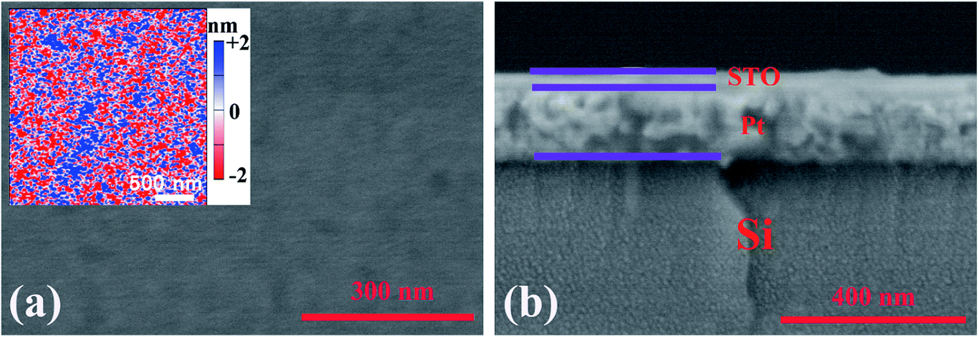 | ||
| Fig. 1 (a) SEM image for the surface of STO/Pt. The insert figure in (a) is the surface measured by AFM (3 μm × 3 μm). (b) SEM image for the cross section of STO/Pt. | ||
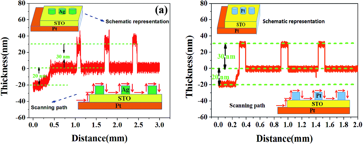 | ||
| Fig. 2 (a) The step changes of Ag/STO/Pt films. (b) The step changes of Pt/STO/Pt films. The insert figures show the schematic representation and the scanning path. | ||
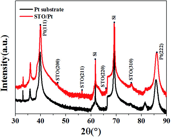 | ||
| Fig. 3 XRD patterns of STO/Pt heterostructure and Pt substrate at various 2θ. | ||
I–V characteristics of the Ag/STO/Pt and Pt/STO/Pt memory cells were studied by voltage sweep measurements to evaluate the memory effects of the obtained devices, and the results are illustrated in semilogarithmic scales, as shown in Fig. 4(a). The corresponding current is measured at voltage (V) with V sweeping in a sequence of 0 V → positive voltage → 0 V → negative voltage → 0 V. The devices show rectifying and hysteretic I–V characteristics indicative of resistive switching. During the measurements, a forming process was necessary for activating the memory effect in the device with Ag top electrode, while current compliance is not necessary. In the device with Pt top electrode, no forming process was needed to activate the device, while current compliance was very necessary to protect the memory cell. Too large current in the device with Pt top electrode can also cause the resistive switching, but the resistive switching is irreversible.
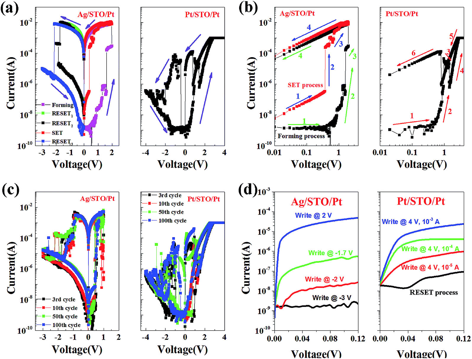 | ||
| Fig. 4 (a) Current of Ag/STO/Pt and Pt/STO/Pt devices at various applied voltage. (b) The forming process and SET process of Ag/STO/Pt device and Pt/STO/Pt device. (c) Current of the devices after different endurance tests. (d) Multi-states of Ag/STO/Pt and Pt/STO/Pt device after different write processes. The middle states are achieved by voltage pulses in the Ag/STO/Pt device, while the others are achieved by voltage sweepings. The OFF state Pt/STO/Pt device is achieved after the process of RESET process, the other states of Pt/STO/Pt device are achieved after SET processes with current compliance of 10−5 A, 10−4 A, 10−3 A, respectively. | ||
As shown in the Fig. 4(a), after the forming process of 0 V → +2 V → 0 V, the Ag/STO/Pt stays at ON state. Then a RESET1 process of 0 V → −1.5 V → 0 V was applied on the device, but the device still stays at ON state. When a RESET2 process of 0 V → −2 V → 0 V was applied on the device, the device was back to the OFF state, but the resistance of device is lower than the former OFF state. Then a SET process like the forming process is applied on the device, the device turned to ON state again, but the curve was very different from the curve of forming process. When RESET3 process of 0 V → −3 V → 0 V was applied on the device, the device was back to OFF state again. All these show that the device with Ag top electrode needs the forming process, but the forming process can be same to the SET process (the way of voltage applied is the same). Different RESET process may result in different resistance state in Ag/STO/Pt device, implying multilevel date storage.
In the measurement of Pt/STO/Pt device, the voltage was swept in a sequence of 0 V → +4 V → 0 V → −4 V → 0 V. By steady increase of the positive voltages imposed on the device, a pronounced change of resistance from the OFF state to ON state was observed at about 1 V, which is called the “SET” process. However, in the effect of negative voltage, the ON state turned to OFF state in a gentle change. The gentle change shows that the resistance of Pt/STO/Pt can be tuned in a large range. Important thing is that the current of the device is very low in the process of 0 V → −0.4 V, it may be caused by the unstable conductive path.
The I–V curves of forming process or SET process of these devices are shown in Fig. 4(b), in which the voltage values are in logarithmic form. The forming process or SET process of Ag/STO/Pt memory cell can be divided into four steps. However, the SET process of Pt/STO/Pt is much more complicated, and it contains six steps. As were reported, the migration of oxygen vacancies (or oxygen ions) under an applied electrical field plays an important role in the metal oxide materials.12–16,22,23 And based on the investigations of the former reports, the resistive switching effects in our case are mediated by filament. The active mediums are in fact much smaller than the cell size, providing a potential of scaling. Ag might be migrating much more positive in Ag/STO/Pt device, oxygen ions and oxygen vacancies are migrating much more positive in Pt/STO/Pt device. Furthermore, the slopes of 4th step in Ag/STO/Pt and the 6th step in Pt/STO/Pt are almost the same, and the resistance of Ag/STO/Pt at ON state is much lower than the resistance of Pt/STO/Pt at ON state, and all these also mean that the conductive filaments in the two devices are different.
In Ag/STO/Pt device, when the positive voltage is applied on the device, oxidation occurs on Ag which is an electrochemically active material.5 Therefore Ag+ cations are generated, which could be described as Ag → Ag+ + e−. The mobile Ag+ cations migrate toward Pt electrode through the STO layer and are reduced there by electrons flowing from the cathode, i.e., Ag+ + e− → Ag. In the effect of negative electric field, the Ag ions can migrate back to Ag electrode in the same way.5
In Pt/STO/Pt device, the oxygen vacancies are like positive ions, when the positive voltage is applied on the device, they can migrate in the STO film and form the oxygen vacancy filament.24 The oxygen vacancy filament may be destroyed when the negative voltage is applied on the device.12–16 Although the resistive switching is only caused by the oxygen vacancies in the STO film, the switching ratio is relatively high. As shown in the former articles, the Ti/Fe:STO/Nb:STO device also shows a filamentary resistive switching phenomenon, induced by the redox-reaction at the Ti/SrTiO3 interface.25 And such resistive switching phenomenon can also been observed in NiO and PZT thin films device with special metal electrodes.26,27 But in Ti/Fe:STO/Nb:STO device or NiO and PZT thin films device with special metal electrodes, the resistive switching is caused by the oxygen vacancies in these films and the oxygen vacancies formed by redox-reaction at interface. However, the switching ratio and operating voltage of our device are all better than these devices.
In the device of Ag/STO/Pt, both the first steps of forming and SET processes are based on the semiconductor conduction mechanism, and the resistance is relatively high. The second steps are the resistance mutations because of conductive filament formation. The third steps are unstable conductive filament stage because the conductive filament is not very stable. The last steps are the stable conductive filament stage because the Ag filament is strong enough and the conductive filament is stable. In the device of Pt/STO/Pt, the first step is also based on the semiconductor conduction mechanism, but the conductive filament can only forms after the steps from 2nd to 6th. It is very clear that the formation of conductive filament in Pt/STO/Pt is so complicated, the current changes very strange as the changing of applied voltage, as shown in the Fig. 4(b).
In order to investigate the repeatability, we swept the Ag/STO/Pt memory cell by voltage sweeping of 0 V → +1 V → 0 V → −3 V → 0 V, and swept the Pt/STO/Pt memory cell by voltage sweeping of 0 V → +4 V → 0 V → −4 V → 0 V for 100 times with current compliance of 10−3 A. The 3rd, 10th, 50th and 100th I–V curves of Ag/STO/Pt and Pt/STO/Pt memory cell are shown in Fig. 4(c). The OFF/ON resistance ratio of Ag/STO/Pt is high to about 106–108%, and the OFF/ON resistance ratio of Pt/STO/Pt is high to about 105–107% in the 100 times. All these ratios are relative high comparing with the resistive switching memory cells based on STO films,17–21 making the periphery circuit very easy to distinguish the storage information (‘1’ or ‘0’). In the repeatability tests, the resistance state of Pt/STO/Pt is not stable when the voltage is sweeping from 0 V to −0.4 V, but the resistance states can be distinguished clearly when low positive voltage is applied on it to read the state.
Both the Ag/STO/Pt device and Pt/STO/Pt device can achieve four resistance states by applied different SET processes, as shown in Fig. 4(d). The middle states are achieved by voltage pulses in the Ag/STO/Pt device, while the others are achieved by voltage sweepings. In the multi-states test of Ag/STO/Pt, a voltage sweeping of 0 V → 2 V (forming process) or 0 V → 1 V (SET process) was first applied to get the ′3′ (ON state, low resistance state), then a voltage pulse of −1.7 V or −2 V was applied, it turned to ‘2’ or ‘1’. And after a voltage sweeping of 0 V → −3 V, it would turn to ‘0’. Based on the former discussion, the Ag filament is dominant in the Ag/STO/Pt device. The initial state achieving middle states is ON state of Ag/STO/Pt device. The time of voltage pulse achieving middle states is about 1–5 μs. In such a short time, the Ag ions in the STO films cannot all migrate back to the Ag electrode with such a low voltage, because the formation or destruction of Ag filament always needs a voltage sweeping.5 So we suppose that the voltage pulse only changed the shape of the Ag filament. The ‘1’, ‘2’ and ‘3’ could be achieved by 0 → 4 V voltage sweepings with current compliances of 10−5 A, 10−4 A and 10−3 A in the device of Pt/STO/Pt, however, the device should be turned to ‘0’ first in the write processes of the middle states (‘1’ and ‘2’). While oxygen vacancy migration is dominant in the Pt/STO/Pt device, the voltage sweeping with different current compliances can tune the migration distance of the oxygen vacancies, the different migration distances caused the four states of the device.22 The initial state achieving the middle state in Pt/STO/Pt device is OFF state. It may prove the different mechanisms of middle states, because the initial states achieving the middle states in the two devices are different. The possible mechanisms are shown clearly in Fig. 5. These intermediate states prove that the devices are not only resistive switching memories but also memristors. One interesting thing is that the middle states can also be achieved by voltage sweepings in the Ag/STO/Pt device, as the middle state shown in the Fig. 4(d), however, the middle states achieved by this way has little repeatability, so we did not investigate in detail, and the write way using voltage pulse contribute to the ultrafast writing. Comparison of the devices with polycrystalline/crystalline STO films in Table 1 shows that the performance of Ag/STO(20 nm)Pt device is much better.
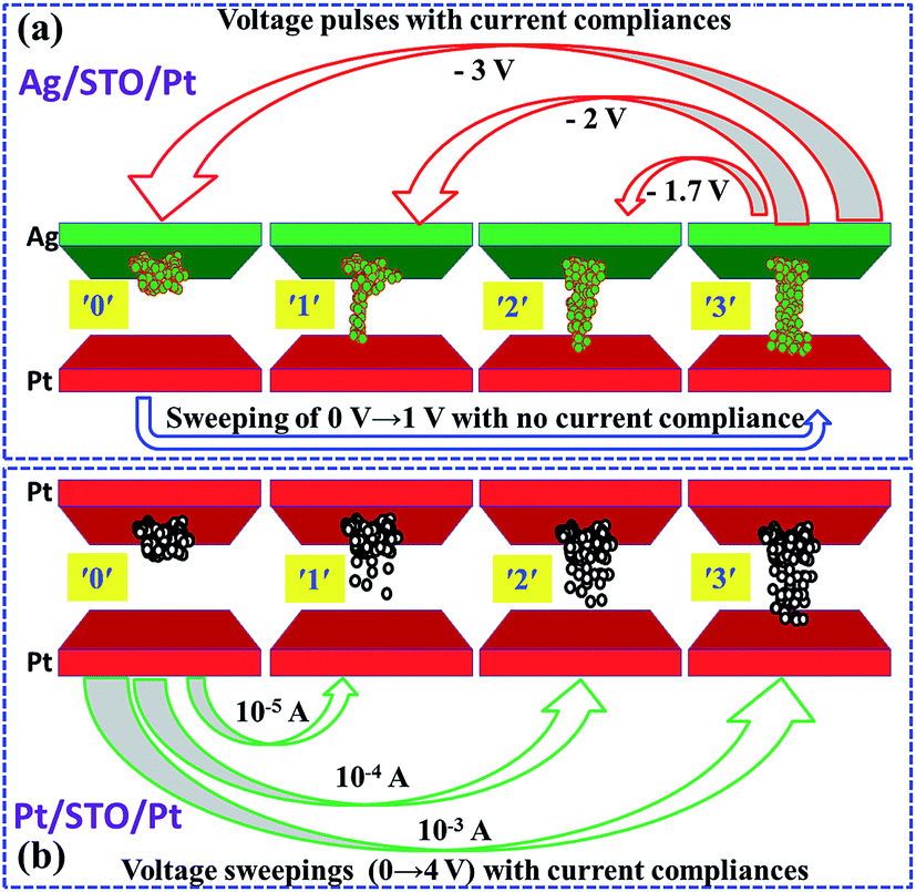 | ||
| Fig. 5 The different resistive switching mechanisms of Ag/STO/Pt device (a) and Pt/STO/Pt device (b). The red arrows show that the multilevel states of Ag/STO/Pt device are achieved by the voltage pulses after the SET processes, and the blue arrow shows that the ‘0’ can turn to the ‘3’ state using voltage sweeping with no current compliance. The green arrows show the multilevel states of Pt/STO/Pt are achieved by voltage sweepings with different current compliances after the RESET processes. | ||
| Device | Crystalline STO film | Top electrode | SET voltage | Reset voltage | Switching ratio | Resistance state | Ref. |
|---|---|---|---|---|---|---|---|
| Fe:STO(200 nm)/Nb:STO | Yes | Pt | ∼2.5 V | ∼−2.5 V | 60 | 2 | 18 |
| STO/SRO | Yes | Pt | ∼2 V | ∼−2 V | ∼100 | 2 | 24 |
| STO(10 nm)/SRO | Yes | — | >−4 V | >−4 V | ∼10![[thin space (1/6-em)]](https://www.rsc.org/images/entities/char_2009.gif) 000 000 |
2 | 28 |
| Ba:STO(100 nm)/SRO | Yes | Pt | >−3 V | >4 V | ∼3 | 2 | 29 |
| STO(20 nm)/Pt | No | Pt | ∼3 V | ∼−4 V | ∼10000 |
4 | — |
| STO(20 nm)/Pt | No | Ag | ∼1 V | ∼−3 V | ∼100000 | 4 | — |
Retention is an important issue for the nonvolatile memory cells. The different resistance states of the devices were set as the former processes, respectively. All the resistance states are read at 0.2 V. After 24 hours, there are not many differences with the beginnings, as shown in Fig. 6. So the two devices have good retention properties. An important thing is that the lowest resistance of Ag/STO/Pt is higher than the lowest resistance of Pt/STO/Pt, it may be caused by the Ag ions which do not migrate back to the Ag electrode.
 | ||
| Fig. 6 Retention of the devices. Current as a function of time. All the resistance states are read at 0.2 V. (a) Ag/STO/Pt. (b) Pt/STO/Pt. | ||
4. Conclusion
In summary, we have fabricated STO thin film based memories with different top electrodes. The migration of Ag/oxygen vacancy causes the resistive switching in the effect of external electric field. And we find the switching ratio of STO thin film memory with Ag top electrode can be high to about 107%, and the switching ratio of STO thin film memory with Pt top electrode can be high to about 106%. How to write the intermediate states using much easier ways may be new problems to apply the devices, but taking retention characteristics, these excellent switching performances and the potential of being multi-states memory into consideration, the STO based memory devices show strong promise for future nonvolatile resistive switching memory applications.Conflicts of interest
There are no conflicts to declare.References
- G. I. Meijer, Science, 2008, 319, 1625 CrossRef CAS PubMed.
- Y. Dong, G. Yu, M. C. McAlpine, W. Lu and C. M. Lieber, Nano Lett., 2008, 8, 386 CrossRef CAS PubMed.
- W. Lu and C. M. Lieber, Nat. Mater., 2007, 6, 841 CrossRef CAS PubMed.
- S. Yuan, Z. Yang, C. Xie, F. Yan, J. Dai, S. P. Lau, H. L. W. Chan and J. Hao, Adv. Mater., 2016, 28(45), 10048–10054 CrossRef CAS PubMed.
- Y. C. Yang, F. Pan, Q. Liu, M. Liu and F. Zeng, Nano Lett., 2009, 9, 1636 CrossRef CAS PubMed.
- C. H. Huang, J. S. Huang, S. M. Lin, W. Y. Chang, J. H. He and Y. L. Chueh, ACS Nano, 2012, 6, 8407 CrossRef CAS PubMed.
- D.-H. Kwon, K. M. Kim, J. H. Jang, J. M. Jeon, M. H. Lee, G. n. H. Kim, X. S. Li, G. S. Park, B. Lee, S. Han, M. Kim and C. S. Hwang, Nat. Nanotechnol., 2010, 5, 148 CrossRef CAS PubMed.
- H. Shima, F. Takano, H. Akinaga, Y. Tamai, I. H. Inoue and H. Takagi, Appl. Phys. Lett., 2007, 91, 012901 CrossRef.
- H. Shima, N. Zhong and H. Akinaga, Appl. Phys. Lett., 2009, 94, 082905 CrossRef.
- R. Waser and M. Aono, Nat. Mater., 2007, 6, 833 CrossRef CAS PubMed.
- S. Q. Liu, N. J. Wu and A. Ignatiev, Appl. Phys. Lett., 2000, 76, 2749 CrossRef CAS.
- C. Ederer and N. A. Spaldin, Phys. Rev. B: Condens. Matter Mater. Phys., 2005, 71, 224103 CrossRef.
- R. Waser and M. Aono, Nat. Mater., 2007, 6, 833–840 CrossRef CAS PubMed.
- A. Sawa, Mater. Today, 2008, 11, 28–36 CrossRef CAS.
- R. Waser, R. Dittmann, G. Staikov and K. Szot, Adv. Mater., 2009, 21, 2632 CrossRef CAS.
- C. H. Huang, J. S. Huang, S. M. Lin, W. Y. Chang, J. H. He and Y. L. Chueh, ACS Nano, 2012, 6, 8407 CrossRef CAS PubMed.
- H. Nili, S. Walia, S. Balendhran, D. B. Strukov, M. Bhaskaran and S. Sriram, Adv. Funct. Mater., 2014, 24(43), 6741–6750 CrossRef CAS.
- T. Menke, P. Meuffels, R. Dittmann, K. Szot and R. Waser, J. Appl. Phys., 2009, 105, 066104 CrossRef.
- K. M. Kim, B. J. Choi, M. H. Lee, G. H. Kim, S. J. Song, J. Y. Seok, J. H. Yoon, S. Han and C. S. Hwang, Nanotechnology, 2011, 22, 254010 CrossRef PubMed.
- S. B. Lee, J. S. Lee, S. H. Chang, H. K. Yoo, B. S. Kang, B. Kahng, M.-J. Lee, C. J. Kim and T. W. Noh, Appl. Phys. Lett., 2011, 98, 033502 CrossRef.
- X. Sun, G. Li, L. Chen, Z. Shi and W. Zhang, Nanoscale Res. Lett., 2011, 6, 599 CrossRef PubMed.
- H. N. Ahmadabadi, T. Ahmed and S. Walia, Nanotechnology, 2016, 27(50), 1–8 Search PubMed.
- P. Hou, J. Wang and X. Zhong, RSC Adv., 2016, 6, 81789 RSC.
- M. C. Ni, S. M. Guo and H. F. Tian, et al., Appl. Phys. Lett., 2007, 91(18), 183502 CrossRef.
- S. Stille, C. Lenser, R. Dittmann, A. Koehl, I. Krug, R. Muenstermann, J. Perlich, C. M. Schneider, U. Klemradt and R. Waser, Appl. Phys. Lett., 2012, 100, 223503 CrossRef.
- C. B. Lee, B. S. Kang, A. Benayad, M. J. Lee, S.-E. Ahn, K. H. Kim, G. Stefanovich, Y. Park and I. K. Yoo, Appl. Phys. Lett., 2008, 93, 042115 CrossRef.
- P. Hou, J. Wang, X. Zhong and Y. Wu, RSC Adv., 2016, 6, 54113 RSC.
- K. Szot, R. Dittmann and W. Speier, Phys. Status Solidi RRL, 2007, 1(2), 86–88 CrossRef.
- R. Oligschlaeger, R. Waser and R. Meyer, Appl. Phys. Lett., 2006, 88(4), 042901 CrossRef.
| This journal is © The Royal Society of Chemistry 2017 |