
 Open Access Article
 This Open Access Article is licensed under a
 Creative Commons Attribution 3.0 Unported Licence
Insights into the heterogeneous distribution of SERS effect in plasmonic hot spots between Au@SiO2 monolayer film and gold single crystal plates†
Chao Wei,
Chenjie Zhang,
Jing Zhang,
Minmin Xu,
Yaxian Yuan and
Jianlin Yao *
*
College of Chemistry, Chemical Engineering and Materials Science, Soochow University, Suzhou, 215123, China. E-mail: jlyao@suda.edu.cn
First published on 16th October 2017
Abstract
Plasmonic hot spots, capable of confining strong electromagnetic fields near metallic surfaces, are particularly essential to a variety of enhanced spectroscopic techniques. Understanding the electric field distributions in the hot spot plays a crucial role in controlling the fabrication of plasmonic nanostructures for a variety of plasmon-based applications. The investigation of plasmonic hot spots in metallic nanosystems has not been fully evaluated. Here, we develop a facile approach by experimental means for investigating the distribution of plasmonic hot spots in surface-enhanced Raman spectroscopy (SERS) based on the dual-probe strategy by coupling a p-mercaptobenzoic acid-embedded Au@SiO2 ((Au-pMBA)@SiO2) nanoparticle monolayer film with thiophenol-modified gold single crystal plates (TP-GSCPs). We demonstrated, for the first time, the heterogeneous distribution of SERS effect in the gap between Au@SiO2 monolayer film and GSCPs. As increasing the gap distance by changing the thickness of silica spacer, the SERS effect of the probe on the gold nanoparticles decayed with a slower rate than that of the other probe attached onto the GSCPs. It mainly originated from the difference of localized dielectric environments and curvatures. By deliberately controlling the silica shell thickness, the switchable plasmonic coupling effect can be achieved between “particle–particle” gap mode and “particle-surface” gap mode. The results reveal that the transfer effect is more evident for (Au-pMBA)@SiO2 films with thinner silica shell thickness and for 785 nm illumination as excitation wavelength than 633 nm. Moreover, the introduction of NaOH solution to (Au-pMBA)@SiO2 films leads to the transfer of the hot spots to the areas between neighboring nanoparticles again due to the removal and dissolution of silica shells. The understanding gained from our experimental observation provides keen insight into the plasmonic hot spots in coupled nanostructures, offering guidance for rational design of plasmonic substrates for ultrasensitive SERS detections.
Introduction
Since its discovery in the 1970s,1,2 surface-enhanced Raman spectroscopy (SERS), as a molecular vibrational spectroscopic technique, has attracted much research interest in the field of surface science due to its high sensitivity and surface selectivity, as well as unique capability of providing detailed surface information of gathering state of nanoparticle SERS substrates,3 adsorption mode and orientation,4,5 and adsorption environment6 of adsorbed molecules. However, the poor generality and spatial resolution still brought lots of restrictions on the fundamental investigation and practical application. With the fast development of nanotechnology, tip-enhanced Raman spectroscopy (TERS)7–9 and shell-isolated nanoparticle-enhanced Raman spectroscopy (SHINERS)10 were successively proposed in the last few decades, which extended the universality and flexibility of SERS substrate for the relevant studies on diverse surfaces, involving smooth or even single crystal surfaces. Till now, enhancement mechanisms mainly include electromagnetic (EM) and charge transfer (CT) enhancement.11,12 EM enhancement is well recognized due to the notable surface plasmon resonance (SPR) effect in the near field of metallic surface, which makes the dominant contributions to SERS signals.13 In fact, the electromagnetic field intensity distributions are not uniform in different surface areas. As we know, plasmonic hot spots located in the small gaps of particle aggregates make the leading contributions to SERS signals in the previous studies.14,15 Generally, hot spot areas can be formed by coupled metallic nanostructures such as metal aggregates or particle-metal substrates with surface plasmons (SPs), generating huge enhanced SERS effects within the areas.16,17 As these plasmonic hot spots are usually randomly distributed, the fundamental understanding of coupling effect in metallic systems is of great significance for design and fabrication of substrates with high SERS activities. Although considerable efforts have been made, the knowledge of plasmonic hot spots distributions for SERS in coupled metallic system is still far from being complete. To this end, the search of a suitable metallic system as theoretical model is highly desired.The metallic single crystal surface-metallic nanoparticle system is a reasonable candidate for monitoring the distribution of plasmonic hot spots. Compared with polycrystalline nanoparticles (NPs), gold single crystal plates (GSCPs), a kind of two-dimensional metallic material, which have large atomically-flat surfaces, are more suitable for the fabrication of theoretical models and hold a great promise in catalytic fields18–20 due to the benign catalytic activities of gold for some crystal face-dependent catalytic reactions. The chemical-synthesized GSCPs also replace expensive traditional single crystal electrodes, to a certain extent, to study molecular adsorption behaviors on single crystal surfaces. Unfortunately, such single crystal metallic surfaces often suffer from weak SERS behaviors21 due to the mismatch of the optical wave vectors, which leads to no breakthroughs for a long time. Until the recent discovery of SHINERS technique which couples an inert shell-coated metallic NP film with single crystal surface,10 new vitalities of SERS study for investigating molecular adsorption behaviors and in situ monitoring catalytic reactions on single crystal surfaces were inspired again. The ultrathin and compact pinhole-free inert silica or alumina shells covered on the surfaces of SERS-active gold or silver NPs isolate the inner NPs from the surroundings outside, prevent the direct contact of NPs with molecules on substrates and inhibit the charge transfer between NPs and substrates.10,21 Here the inner NPs are only served as electromagnetic enhancement as well as Raman signal amplification sources for accurately reflecting the adsorption behaviors of molecules on single crystal surfaces in the SHINERS model. Although single crystal surfaces cannot provide effective localized surface plasmon resonance (LSPR) enhancement signals for SERS detections, propagating surface plasmon polaritons (PSPPs) can be excited by certain means such as Otto model and Kretschmann model,22 and propagate parallel to the single crystal surfaces to enhance the SERS signals of adsorbed molecules to a certain extent.
In such coupled system, hot spot coupling effects can be generated in the areas of gaps of either neighboring NPs in metallic dimers or NP-metallic substrates. The latter coupling effect not only includes PSPPs generated on the surfaces of substrates coupling with LSPR generated on the surfaces of NPs, but also particles themselves coupling with their mirror images formed on the surfaces of substrates similar to dimers due to the image field effect.23,24 In addition, the coupling degree of this model is closely related to the gap distances between the two25,26 and the dielectric constants around the substrates.27 For example, the dielectric environment is distinctly different for core–shell metallic NPs from the naked ones when they are covered on the two-dimensional metallic substrates. Not long ago, Tian's group28–30 performed a series of studies about the hot spot distributions and plasmonic properties of shell-isolated nanoparticles (SHINs) on smooth gold (or silver) substrates. The results indicate that compared with naked metallic gold (or silver) NPs, the silica shell of SHINs inserting between the NP and the single crystal substrate can prevent the spread of free electrons from the surface of NP to the substrate, which will greatly reduce the quality factor of the SPR for the NP through the NP-substrate interface and finally induce the accumulation of free electric charges for generating a pretty strong electric field as well as the formation of coupling effect in the gap of the contact interface to make a hot spot that can provide extremely high enhancement locally when they are covered on the surface of single crystal substrate based on the three-dimensional finite-difference time-domain (3D-FDTD) simulations. That is to say, the plasmonic hot spots transfer from the areas between neighboring NPs to those between upper NPs and lower substrate, i.e. the hot spot coupling form transforms from “particle–particle” to “particle-surface” gap mode.
The discovery of this phenomenon makes the application of SHINs more rewarding in the detection of molecules adsorbed on smooth or non-active substrates due to the generation of hot spots in the gap which is in favor of the enhancement of SERS signals, but the research of hot spot distribution of NP-substrate coupled system mainly focuses on the theoretical simulation so far. To this end, a new type of plasmonic model system based on probe-embedded gold core-silica shell structures coupled with smooth metallic substrates such as GSCPs for signal monitoring with different shell thicknesses and gap distances needs to be developed for better understanding the hot spot distributions clearly by experimental means. Furthermore, as the plasmonic hot spots are randomly distributed, for the hot spot areas of “particle-surface” gap mode between GSCPs and gold NPs (GNPs), the electromagnetic field distribution may be non-uniform and the variation of silica shell thickness also leads to different coupling effects inside or outside the shells due to their different localized dielectric environments. Therefore, another kind of SERS probe molecule needs to be assembled on the plates in advance to reflect the electromagnetic field intensities outside of the silica shells, and the understanding of plasmonic hot spots is of great significance for rationally designing this novel nanostructure with improved SHINERS technology. The SERS signals of the two kinds of probe molecules can be simultaneously detected through the coupling effects between upper NPs and lower plates.
Herein, p-mercaptobenzoic acid (pMBA), embedded in the gaps between gold core and silica shell, was selected as a probe molecule for internal reference. The model of corresponding monolayer film structures of the formed (Au-pMBA)@SiO2 NPs coupled with GSCPs was designed and fabricated rationally to investigate their hot spot distributions. Likewise, thiophenol (TP), accompanying with pMBA, was chosen as another probe molecule outside of the silica shells and modified on the surfaces of GSCPs for monitoring the SERS signal of the gap areas between upper NPs and lower substrate on both sides of the silica shells. By comparing the change in SERS intensity of the two kinds of probe molecules, we demonstrate the switching of plasmonic hot spots between “particle–particle” and “particle-surface” gap mode in response to the variation of silica shell thickness. Moreover, the removal and dissolution of silica shells were preliminarily attempted to investigate the variations of hot spot distributions of (Au-pMBA)@SiO2 films on GSCPs by the introduction of NaOH solution.
Experimental section
Reagents
Chloroauric acid tetrahydrate (HAuCl4·4H2O), trisodium citrate dihydrate (Na3C6H5O7·2H2O), toluene (C6H5CH3), acetone (CH3COCH3), hydroquinone (C6H6O2), N,N-dimethylformamide (DMF, C3H7NO) and the relevant chemicals were purchased from Sinopharm Chemical Reagent Co., Ltd; thiophenol (TP, C6H5SH) and p-mercaptobenzoic acid (pMBA, C7H6O2S) were acquired from Tokyo Chemical industry Co., Ltd; p-nitrothiophenol (pNTP, C6H5NO2S) was obtained from Matrix Scientific; mercaptopropyltrimethoxysilane (MPTMS, C6H16SSiO3) was acquired from J&K Scientific Ltd; 1,5-pentanediol (C5H12O2) was purchased from Acros Organics; pyridine (Py, C5H5N), polyvinylpyrrolidone (PVP, MW ≈ 40![[thin space (1/6-em)]](https://www.rsc.org/images/entities/char_2009.gif) 000) and sodium silicate (Na2SiO3) were obtained from Sigma-Aldrich.
000) and sodium silicate (Na2SiO3) were obtained from Sigma-Aldrich.
All aqueous solutions were prepared using Milli-Q water (resistivity ≥ 18 MΩ cm).
Preparation of metallic NPs and plates
15 nm of GNPs seeds were prepared according to Frens's method.31 Typically, 2 mL of trisodium citrate solution (1.14 wt%) was added to 100 mL of HAuCl4 solution (0.01 wt%) when the system was heated to boiling under vigorous stirring. The mixture was cooled down to ambient temperature naturally after the next 15 min since the colour of the colloid turned to orange red.110 nm of GNPs were synthesized through seed-mediated growth method by using 15 nm of GNPs as seeds. The preparation approach was referred to Li's method32 using hydroquinone as reductant. Briefly, 400 μL of the prepared seed solution was added to 96 mL of Milli-Q water, followed by the addition of 220 μL of trisodium citrate solution (1.14 wt%) and 1 mL of HAuCl4 solution (1 wt%). Subsequently, 1 mL of hydroquinone solution (3.3 mg mL−1) was added quickly under vigorous stirring. The solution was kept stirring for about 1 h until the colour changed to khaki which marked the formation of final GNPs. In this process, hydroquinone as the reductant could further reduce the citrate-reduced AuI to Au0 which was beneficial for the secondary growth on the surfaces of seeds. The resulting solution was kept overnight and then boiled at 90 °C for about 30 min to remove the superfluous reductant in reserve.
GSCPs were synthesized according to a modified literature's protocol.33,34 Briefly, 600 mg of PVP powder was first dissolved in 9 mL of 1,5-pentanediol under ultrasonication. Then the mixture was heated to 160 °C, followed by the rapid addition of 1 mL of HAuCl4 solution (10 wt%). The yellow colour of the solution gradually faded away, accompanied by the appearance of a large number of shiny reddish brown granular materials, indicating the formation of GSCPs. The solution was cooled down by ice water bath rapidly after another 45 min, then it was centrifugated and rinsed with acetone and ethanol successively for four times. The resulting products in the sediment were filtered and dispersed in ethanol finally for further use.
The (Au-pMBA)@SiO2 core–shell nanoparticles (CSNPs) were prepared by hydrolysis of Na2SiO3 solution in boiling water bath similar to the synthesis method of SHINs.10 The only difference was the modification of pMBA to the gold colloid before the encapsulation of SiO2 shell. In a typical process, 15 μL of pMBA ethanol solution (1 mmol L−1) was added to 10 mL of the as-prepared gold colloidal suspension under vigorous stirring for about 30 min, followed by the addition of 135 μL of MPTMS ethanol solution (1 mmol L−1). After 15 min, 1080 μL of Na2SiO3 solution (0.54 wt%, pH = 10.5) was added and kept for 3 min. Subsequently, the mixture solution was transferred to a water bath pot, quickly heated to 96 °C under stirring for a period of time and then cooled down to ambient temperature rapidly by ice water bath. The resulting NPs were centrifugated, rinsed with water for three times and finally resuspended by Milli-Q water to the original volume in reserve.
Self-assembly of (Au-pMBA)@SiO2 films
(Au-pMBA)@SiO2 nanoparticle monolayer film (NMF) was prepared through a liquid–liquid two-phase interface method whose oil phase was toluene and whose assistants were DMF and acetone according to the previous work in our group for the preparation of Au@SiO2 films.35 Briefly, 2 mL of (Au-pMBA)@SiO2 colloid and 400 μL of toluene were added successively in a 10 mL of beaker (i.e. the volume ratio of water phase to oil phase was 5:1), as toluene was lighter than water, a distinct water-oil two-phase interface which contained upper toluene and lower (Au-pMBA)@SiO2 colloid would form. Afterwards DMF was added along the beaker wall dropwise. DMF would get into the oil phase at first to make it turbid and then penetrate into the water phase to reduce the electrostatic interaction as well as alter the wettability of surfaces of (Au-pMBA)@SiO2 NPs which would induce their movement from the water phase to the oil phase. When they got to the interface of the two phases with the lowest barrier energy which was conducive to their retention, the NPs could be captured on the interface. With the increased quantity of DMF, the number of captured particles would also increase to have a tendency to form a monolayer until the interface couldn't accommodate more particles. In our present case, it was found that the maximum volume of DMF needed was about 600 μL. After 1 min, acetone was then added slowly along the beaker wall. Under the effect of surface tension, the loose film on the interface would be dense and clear, besides that the turbid oil phase turned to be transparent again. Then an ophthalmic forceps was introduced to clamp both sides of a silicon wafer and pull the formed film at an angle of close to 0° upward from the liquid–liquid two-phase interface. After the residual organic solvents in the oil phase volatilized naturally, the silicon wafer covered by the film was rinsed with ethanol several times for SERS detection.
Construction of (Au-pMBA)@SiO2 film-GSCPs coupled system
The (Au-pMBA)@SiO2 NMF-GSCPs coupled model was constructed by the following method. A certain amount of GSCP ethanol solution was dropped onto a clean silicon wafer. After being exposed to the air for natural drying, it was covered by a (Au-pMBA)@SiO2 NMF as before. This model could be used for SERS detection on both surfaces of silicon wafers and GSCPs to investigate the influences of GSCPs on the hot spot coupling modes of (Au-pMBA)@SiO2 films. In addition, another model which was similar to the former one except that the GSCPs had been modified with another probe molecule (such as TP) by immersion in advance was also constructed to investigate the variations of hot spot distributions on both sides of silica shells for “particle-surface” gap mode between upper (Au-pMBA)@SiO2 NPs and lower GSCPs. The self-assembly principle of the latter model was shown in Scheme 1.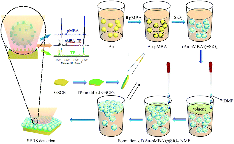 | ||
| Scheme 1 The principle of self-assembly of (Au-pMBA)@SiO2 film on TP-modified GSCP substrate. | ||
SERS measurement
Raman spectra were obtained using a confocal microprobe Raman spectrometer from HORIBA LabRam HR800. The sizes of the slit and pinhole were 100 and 400 μm, respectively. The grating value was 600 gr mm−1. Raman scattering signals were collected by a long working distance 50× objective. A He–Ne laser with a wavelength of 633 nm and a semiconductor laser with a wavelength of 785 nm were selected as excitation sources, respectively. The spectra accumulation time was 10 s. All of the SERS spectra were acquired with the baseline corrections.Results and discussion
Characterizations of NPs, NMFs and GSCPs
Fig. 1 presents a series of local enlarged TEM images of (Au-pMBA)@SiO2 NPs. The reaction time in boiling water bath during the formation of silica shells were 15 min, 30 min, 1 h, 2 h and 3 h, respectively. The final average silica shell thicknesses are about 1.8 nm, 2.5 nm, 5 nm, 6.5 nm and 10 nm, respectively. The silica shells exhibit favorable continuity, completeness and homogeneity for each group of CSNPs. Moreover, with the increase of reaction time, the silica shells keep on growing on the surfaces of GNPs which lead to the increased thicknesses. The TEM image of spherical gold seeds of about 15 nm is shown in Fig. S1,† and TEM images of the core–shell particles and their corresponding cyclic voltammetry curves are shown in Fig. S2 and S3,† respectively. | ||
| Fig. 1 Local enlarged TEM images of (Au-pMBA)@SiO2 NPs synthesized using MPTMS as coupling agent with the silica thicknesses of about 1.8 nm (a), 2.5 nm (b), 5 nm (c), 6.5 nm (d) and 10 nm (e). Scale bar: 20 nm. | ||
Fig. 2 is a series of SEM images of corresponding (Au-pMBA)@SiO2 and (Au-pMBA) NMFs. The NPs on the films which arrange closely with each other display perfect dispersity, and nearly no bilayer or multilayer structures appear from the SEM images. With the increase of silica shell thickness, the average interparticle space increases accordingly due to the existence of the silica shells, which results in the slight difference in compactness. In general, the surface properties of NPs with thicker silica shells are close to those of pure silica spheres which allow to form monolayer array structures.36–38 The continuous silica shells blocked the pinhole effect significantly (see the ESI, Fig. S4†). Therefore, it could be served as a qualified substrate for investigating the distribution of enhancement effect in the gap area for the highly uniform SERS effect it brought.
 | ||
| Fig. 2 SEM images of (Au-pMBA)@SiO2 films with the silica shell thicknesses of about 0 nm (a), 1.8 nm (b), 2.5 nm (c), 5 nm (d), 6.5 nm (e) and 10 nm (f). Scale bar: 500 nm. | ||
Fig. 3 illustrates the top and side view morphologies of GSCPs, together with the selected area electron diffraction (SAED) pattern. The size and thickness of the chemical-synthesized GSCPs, with polygonal structures, are about tens of microns and 200 nm, respectively. Furthermore, through carefully analyzing the SAED pattern, one can conclude unambiguously that the diffraction pattern well fits the structure of (111) crystal face,39 which further demonstrates that the GSCPs only contain (111) crystal faces.
 | ||
| Fig. 3 SEM images of the GSCPs taken from the front (a) and the cross section (b); SAED pattern of the GSCPs (c). Scale bar: 10.0 μm for (a) and 1.00 μm for (b). | ||
Fig. 4 (A) shows the XRD characterization of GSCPs. The main diffraction peak positions for GSCPs are located at the angle of 38.23° and 81.74°, which correspond to the (111) and (222) crystal faces of gold, respectively.40 As the dominant characteristic peak, the diffraction peak of (111) crystal face possesses extremely high intensity and narrow full width at half maximum (FWHM). (222) crystal face is the reflection of the second order peak of (111) crystal face, and both of the two can be regarded as the same one except for the different diffraction angles. The XRD result demonstrates that the synthesized GSCPs almost consist of (111) crystal face and have good crystallinity. Fig. 4 (B) is the SERS spectra of 1 mmol L−1 of pNTP adsorbed on GSCPs with (a) or without (b) Au@SiO2 covering on them. As we know, SPR especially LSPR effect can be only generated on nanoscaled rough metallic surfaces with rich free electrons to enhance the Raman signals, for atomic-level smooth single crystal metallic surfaces, as the mismatch of optical wave vectors, SERS signals of probe molecules absent accordingly.21 Therefore, the absence of SERS features of pNTP further confirms that no SERS contribution is observed on the synthesized GSCPs. The observation of SERS signal of pNTP on Au@SiO2-modified GSCPs mainly originates from the amplification effect of SHINs. As a consequence, the Au@SiO2/GSCPs configuration is qualified as the candidate for investigating the distribution of enhancement contributed solely by the coupling effect between the Au@SiO2 and GSCPs.
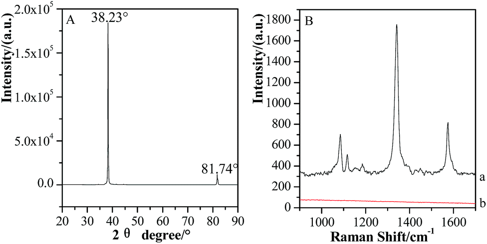 | ||
| Fig. 4 XRD characterization of the GSCPs (A) and SERS spectra of 1 mmol L−1 of pNTP adsorbed on GSCPs with (a) or without (b) Au@SiO2 SHINs (B). | ||
Hot spot distributions of (Au-pMBA)@SiO2 films on GSCPs
After a continuous (Au-pMBA)@SiO2 NMF was transferred to the Si wafer attached with GSCPs, two different areas were obtained, i.e. the GSCPs-NMF and the Si-NMF with distinct boundary. Therefore, two kinds of coupling hot spots (gap modes) contributed to SERS effect, involving the (Au-pMBA)@SiO2-(Au-pMBA)@SiO2 (“particle–particle” gap mode) and (Au-pMBA)@SiO2-GSCPs (“particle-surface” gap mode) configurations. Based on the above two modes, (Au-pMBA)@SiO2 NMFs with the silica shell thicknesses of 0 nm (no encapsulation), 1.8 nm, 2.5 nm, 5 nm, 6.5 nm and 10 nm were transferred onto GSCPs and the corresponding SERS spectra were acquired by using 633 nm or 785 nm laser as excitation line (as shown in Fig. 5). Moreover, the line detections of (Au-pMBA)@SiO2 NMFs through the surfaces of GSCPs illuminated by 633 nm laser are presented in ESI (as shown in Fig. S5†).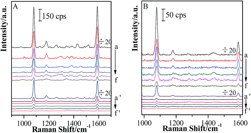 | ||
| Fig. 5 SERS spectra of (Au-pMBA)@SiO2 films of various silica shell thicknesses: 0 nm (a, a′), 1.8 nm (b, b′), 2.5 nm (c, c′), 5 nm (d, d′), 6.5 nm (e, e′) and 10 nm (f, f′) in the areas of (a → f) and beyond (a′ → f′) GSCPs using 633 nm (A) or 785 nm (B) illumination as excitation wavelength. | ||
Two main SERS bands at about 1077 cm−1 and 1588 cm−1 were assigned to ν12 and ν8a aromatic ring vibrational modes of pMBA molecules,41 respectively. Interestingly, the SERS signal intensities of pMBA were stronger in the areas of GSCPs (a → f) than in those beyond GSCPs (a′ → f′) for (Au-pMBA)@SiO2 films all along. Moreover, it was independent of the silica shell thicknesses and excitation wavelengths. In general, for the (Au-pMBA)@SiO2-(Au-pMBA)@SiO2 configuration beyond the area of GSCPs, the SERS signals absolutely originate from the hot spot coupling effect generated by neighboring NPs. Although, the GNPs were modified by the pMBA, the contribution on SERS intensities from molecules beyond the hot spot was reasonable to be negligible. Generally, the hot spot coupling effect is critically dependent on the interparticle space (gap distance). In the present case, due to the existence of silica shells, the notably increased gap distances (double space of silica shell thickness) brought the dramatic damping, resulting in the observation of relatively weak SERS signal. For the “particle-surface” gap mode, the coupling effect between the NPs and GSCPs interface induced by the gathering of free electrons in the gap area allowed the giant enhancement of SERS signal of molecules attached on the GSCPs surface and embedded in the (Au-pMBA)@SiO2. However, it should be pointed out that the enhancement was contributed by the “particle–particle” and “particle-surface” gap modes together, and it is difficult to separate their contributions. Tian and his coworkers performed a series of investigations on the coupling effect between the SHINs and single crystal metallic surface, confirming the transfer of hot spots from the “particle–particle” to “particle-surface” gap mode.28–30 Therefore, the observed stronger SERS signal on the GSCPs surface is mainly contributed by the latter mode.
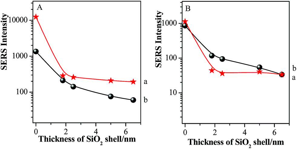
For clear description, the relationships between absolute SERS intensities of pMBA at 1077 cm−1 and silica shell thicknesses in the areas on and beyond GSCPs are presented in Fig. 6.
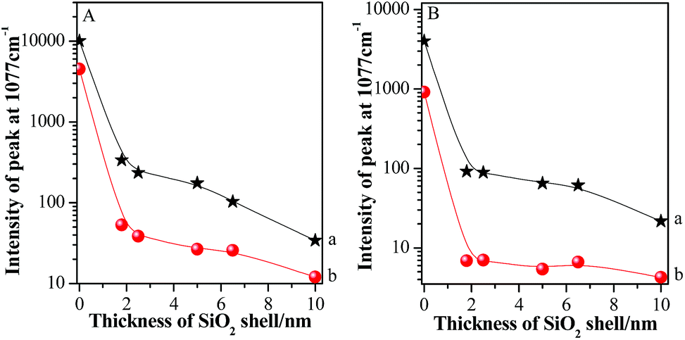 | ||
| Fig. 6 The relationships between silica shell thicknesses and absolute SERS peak intensities of pMBA at 1077 cm−1 using 633 nm (A) or 785 nm (B) illumination as excitation wavelength ((a): GSCPs area; (b): beyond the area of GSCPs). | ||
The Au-pMBA NMF possessed the strongest SERS signal for both gap modes. After the ultrathin silica shells of 1.8 nm thickness were encapsulated on the NPs, the SERS signals of films decreased dramatically, i.e. for the two gap modes, by about 30 and 80 times using 633 nm laser, while by about 40 and 132 times for 785 nm laser, respectively. The larger decrease in SERS intensity for the latter case indicates the effective transfer of hot spots to “particle-surface” gap mode. Furthermore, the decrease rate in SERS intensities on GSCPs surface was slower than that in the area beyond GSCPs, suggesting that the damping effect in coupling of “particle–particle” gap mode caused by the silica shell was complemented by the additional coupling effect from “particle-surface” gap mode. Thus, this fact demonstrates unambiguously that the transfer of hot spots is critically dependent on the wavelength of laser, i.e. associated with SPR of the system. With the further increase of silica shell thickness, the SERS signals continue decreasing to relatively stable values for the increased interparticle distances.42,43
In order to further illustrate the influence of GSCPs on the variation in SERS intensities, the shell thickness-dependent relative SERS intensities (Ibeyond/Ion) from both gap modes are presented in Fig. 7. Ibeyond and Ion are defined as the SERS intensities from the sites beyond or on the GSCPs surface, respectively.
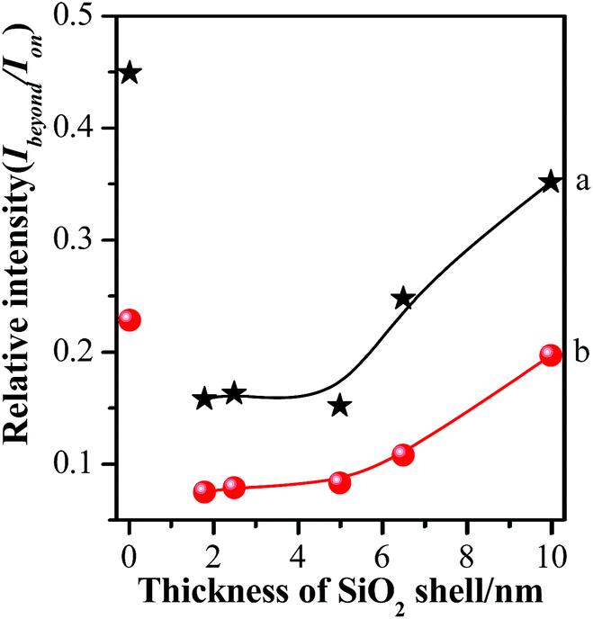 | ||
| Fig. 7 Comparison of relative SERS intensities (Ibeyond/Ion) of various silica shell thicknesses using 633 nm (a) or 785 nm (b) illumination as excitation wavelength. | ||
One can obviously find that the relative SERS intensities are distinctly dependent on the silica shell thicknesses and excitation wavelengths. Here it should be noted that the relative SERS intensity values are less than 1 due to the shorter distance of the “particle-surface” (with single silica shell) than that of “particle–particle” gap mode (with double silica shells). As the laser was switched from the 633 nm to 785 nm, the relative SERS intensities decreased accordingly for each silica shell thickness. It indicates that the latter laser is favorable for the “particle-surface” gap mode. Moreover, the maximum value in the relative SERS intensities was associated with the silica shell-free Au-pMBA NMF. It indicates that the “particle-surface” gap mode does not dominate to contribute to the SERS intensities in the area of GSCPs, i.e. poor transfer of hot spots. It is in good agreement with Tian's investigation on the similar system by experimental and 3D-FDTD simulations,44 in which the delivery and transfer of free electrons resulted in the damping of coupling effect between NPs and single crystal surfaces. As it is well known, the excitation wavelength drives the change in the sizes and phases of lights relative to the particles as well as the gathering states of free electrons on the surfaces.45 Fortunately, the insulated silica shell inhibited the transfer of free electrons and allowed the gathering of them in the “particle-surface” gap area to contribute the strong SERS signal of molecules adsorbed on NPs and single crystal surfaces.28 For the case of 785 nm laser, either the absolute or relative SERS intensities decreased compared with 633 nm laser, especially for the areas of the films beyond the GSCPs whose SERS signals were only contributed by “particle–particle” gap mode of neighboring NPs (within 10 cps for the silica-encapsulated film), indicating that the excitation wavelength matching with the “particle–particle” gap mode is around 633 nm rather than the 785 nm. While the absolute SERS signal disparity by two different excitation wavelengths was significantly reduced for the area on GSCPs. It definitely indicates that the difference in SERS intensity was complemented by the additional coupling effect from “particle-surface” gap mode between upper NPs and lower GSCPs when using 785 nm excitation wavelength, i.e. the 785 nm excitation was crucial in enhancing the electromagnetic field and SERS signals of “particle-surface” gap mode. So one can conclude that the excitation wavelength of the “particle-surface” gap mode matches better with 785 nm rather than the 633 nm. It is consistent with the assumption by comparing the extent of reduction in the absolute SERS intensity after encapsulation of silica shells, and the conclusion also agrees well with the result reported by Chen et al. through theoretical simulations.46 Therefore, it is reasonable to assume that the suitable wavelength for the two gap modes can be determined from the absolute and relative (Ibeyond/Ion) SERS intensities in our present case.
In fact, for the NP-substrate coupled system, the incident light is polarized between the neighboring NP centers, and free electrons on the surface of NPs will undergo oscillation along the axis of particles parallel to the substrate surface, resulting in the dipole coupling effect in this direction at the initial stage. The gathering of free electrons will certainly lead to the formation of positive-charged holes at the bottom of NPs in the “particle-surface” gap. As the GSCPs can be served as a free electron reservoir, it will further induce the charge gathering in the holes underneath the NPs due to the electrostatic effect, causing the redistribution of hot spots on the surfaces to reach a steady and proper state matching with the selected wavelength.30,45 Besides that as the silica shell prevents the spread and transfer of free electrons in the “particle-surface” gap, it is easier to induce the enrichment of charges just in this gap area after the encapsulation of silica shells.28 So one can assume that the laser of 785 nm which matches better with “particle-surface” gap mode is more beneficial to inducing the oscillation of free electrons and thus gathering of charges in the gaps to form electron holes underneath the NPs. The further gathering of charges induced by the holes allows the enhanced electromagnetic field between particles and single crystal surfaces. It finally brings the transformation of coupling effect form from “particle–particle” to “particle-surface” gap mode, and the silica shell plays an essential role in such transformation.
Distributions of enhancement in hot spot area
Based on the above experimental fact, the transformation of hot spot coupling form from “particle–particle” to “particle-surface” gap mode induces the strong enhancement in the gap area. Moreover, the thinner the shell thickness is, the more obvious the transformation is. Although the Raman signal of molecules located in this area is enhanced, the electromagnetic field distribution is non-uniform for both sides of silica shells of “particle-surface” gap mode. Unfortunately, it is quite difficult to clarify this assumption in the nano/subnanoscale gap. Thus, in order to investigate the electromagnetic intensity variations and distributions in the gap under “particle-surface” gap mode, another probe molecule with different SERS features from pMBA was modified on GSCPs surface, and the silica shell with different thicknesses was served as the spacer to regulate the gap distance. For this configuration of (Au-pMBA)@SiO2-TP-GSCPs, two probes were attached onto the two terminals of the gap and separated by the silica shell, i.e. TP on GSCPs and pMBA on GNPs. By comparing the change in the SERS intensities of two probes, one can assume the distribution of electromagnetic field in the gap. Fig. 8 shows the combined SERS spectra of (Au-pMBA)@SiO2 films and TP-modified GSCPs with the silica shell thicknesses of 0 nm (no encapsulation), 1.8 nm, 2.5 nm, 5 nm and 6.5 nm, respectively.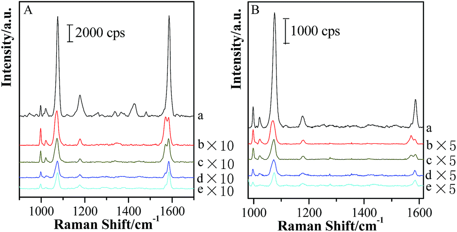 | ||
| Fig. 8 SERS spectra of (Au-pMBA)@SiO2 films of various silica thicknesses: 0 nm (a), 1.8 nm (b), 2.5 nm (c), 5 nm (d) and 6.5 nm (e) covering on TP-modified GSCPs using 633 nm (A) or 785 nm (B) illumination as excitation wavelength. | ||
The main SERS peaks of TP molecules at about 998 cm−1, 1022 cm−1, 1073 cm−1 and 1572 cm−1 were assigned to δr–i–d + νCC, νCC + δCH, νCC + δCH and νCC vibrational modes,47 respectively. The observation of SERS signal from both probes demonstrated that the electric field filled with the gap area. For both laser illuminations, the combined SERS signal exhibited a significant drop (>10 times) after the thin silica shell was attached, and followed a slow decrease process with the increase of the thickness of silica shell. However, the decrease trends for the two kinds of probe molecules were different. Three significant spectral features should be noted as: (i) the SERS intensities of pMBA decreased much faster than those of TP after 1.8 nm SiO2 shell was attached onto pMBA-modified GNPs; (ii) with the further increase of silica shell thickness, the SERS signal intensities of TP decreased rapidly while those of pMBA decreased slowly; (iii) by comparing with the SERS intensities of pMBA, a remarkable increase in SERS intensities of TP was observed as the laser wavelength was switched from 633 nm to 785 nm (as shown in Fig. 9).
 | ||
| Fig. 9 The relationships between silica shell thicknesses and absolute SERS peak intensities of pMBA at about 1588 cm−1 (a) together with TP at about 998 cm−1 (b) using 633 nm (A) or 785 nm (B) illumination as excitation wavelength. | ||
In order to further clarify the origination of change in SERS intensity, the shell thickness-dependent ratios of the SERS intensities of TP at about 998 cm−1 to those of pMBA at about 1588 cm−1 (ITP/IpMBA) profiles are presented in Fig. 10.
 | ||
| Fig. 10 The relationships between silica shell thicknesses and relative SERS peak intensities (ITP/IpMBA) using 633 nm (a) or 785 nm (b) illumination as excitation wavelength. | ||
The values of ITP/IpMBA were relatively low for the Au-pMBA-TP-GSCPs configuration. Although the interfaces between NPs and single crystal plates were isolated by self-assembly layers of TP and pMBA, the thin molecular layers allowed the diffusion and transfer of free electrons, resulting in the very weak electromagnetic field of “particle-surface” gap mode. As a consequence, the “particle–particle” gap mode contributed the dominant hot spot coupling effect on SERS signal. For the present case, pMBA molecules were located in both gap areas of neighboring NPs, and between upper NPs and lower plates, while TP molecules only happened to be located in the gap areas between upper NPs and lower plates. Obviously, the latter gap mode didn't become the dominant hot spot areas in this case. Therefore, it resulted essentially in the relatively low values of ITP/IpMBA.
After the 1.8 nm SiO2 shell was covered onto Au-pMBA NPs, the value of ITP/IpMBA increased rapidly to achieve the maximum, which mainly originated from the decrease of IpMBA or increase of ITP. Both of them demonstrate that the hot spot coupling effect was transformed from “particle–particle” to “particle-surface” gap mode successfully. This transformation of gap modes brought the decrease of SERS intensities of pMBA and increase of those of TP, resulting in the significant increase of relative intensity of ITP/IpMBA. Moreover, for the 785 nm illumination, the ITP/IpMBA value was about three times of that illuminated by 633 nm laser. It definitely suggests that the efficiency of the transformation of gap modes is improved significantly by using the 785 nm laser as excitation line. It is in good agreement with the above-mentioned experimental results. With the further increase of silica shell thickness, the values decreased again gradually and the drop rate was associated with the excitation line, i.e. faster drop for 785 nm than 633 nm (as shown in Fig. 10). Due to the introduction of thicker silica shell, the coupling effect for both gap modes damped dramatically, and thus the SERS signals of pMBA and TP decreased simultaneously. However, the decrease rate for the TP was higher than that of pMBA, i.e. the SERS intensity of TP was more sensitive to the change of the silica shell thickness (as shown in Fig. 9 & 10). Therefore, the relative SERS intensity was decreased with the increase of silica thickness accordingly. It also suggests that the distribution of the electromagnetic field induced by the coupling effect is non-uniform in the area of “particle-surface” gap mode. The high radius of curvature between the NP and the atomically-flat gold interface caused the NPs/GSCPs interface to be curved. The curvatures inside of the shells (NPs side) were higher than those outside (GSCPs side), resulting in that the distributions of electromagnetic fields inclined towards the areas inside (NPs side). As the shell thickness increased, the electromagnetic field intensities damped with a slower rate in the areas inside of the shells, i.e. the pMBA molecules, leading to the smaller values of ITP/IpMBA. Therefore, the electromagnetic field distribution is intuitively understood in “particle-surface” gap mode or even other hot spot coupling effects under various gap distances by the dual-probe strategy.
The effect of removal of silica shells on the SERS signals of (Au-pMBA)@SiO2 films on GSCPs
Based on the above facts, the silica shell plays an essential role in the transformation of gap modes from “particle–particle” to “particle-surface”. Therefore, the removal of silica shells might change the form of coupling effect and recover to the Au-pMBA-GSCPs configuration. Accordingly, the coupling effect of “particle–particle” gap mode would become the domination for SERS enhancements for both lasers. In order to verify this assumption, the (Au-pMBA)@SiO2 (1.8 nm) NMF-covered GSCPs were firstly immersed in NaOH solution overnight and rinsed with Milli-Q water twice to remove the silica shells completely, and then SERS spectra were acquired in the areas on or beyond the GSCPs surface by using 633 nm illumination as excitation wavelength (as shown in Fig. 11 (A)). It should be pointed out that the observation of SERS features of TP at about 998 cm−1 and 1022 cm−1 was mainly due to the surface plasmon-induced catalytic decarboxylic reactions of pMBA molecules on the surfaces of GNPs in alkaline solutions.41,48 Incidentally, the introduction of NaOH solution brought the decrease of metastable-SERS activity of GNPs or resulted in the desorption of pMBA molecules. Both effects caused a significant decrease in SERS signal.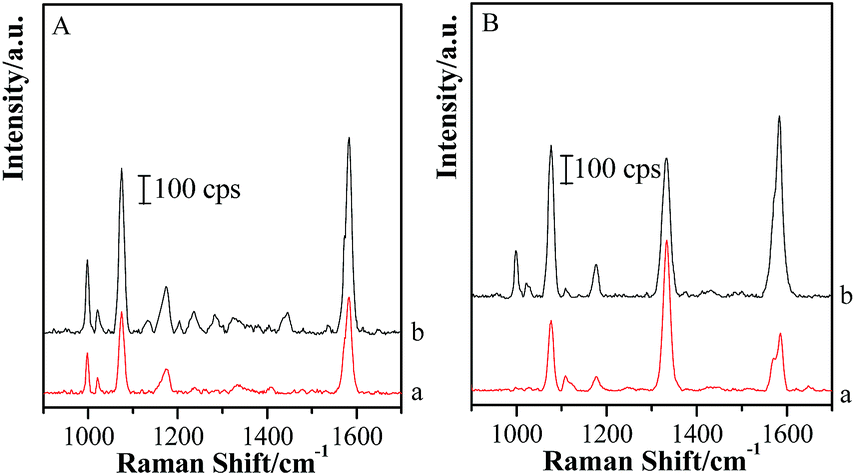 | ||
| Fig. 11 (A) SERS spectra of (Au-pMBA)@SiO2 (1.8 nm) film in the areas on (b) and beyond (a) GSCPs after removing the silica shells. (B) SERS spectra of (Au-pMBA)@SiO2 (1.8 nm) film on the surfaces of pNTP-modified GSCPs after removing the silica shells (b); original film (a). | ||
Based on the above-mentioned fact in Fig. 7, the original relative SERS intensities (Ibeyond/Ion) were about 0.449 and 0.158 for the silica shell thicknesses of 0 nm and 1.8 nm, respectively. After removing the silica shells, the signal intensity of the area on GSCPs (Fig. 11(A, b)) was about two times as strong as that beyond GSCPs (Fig. 11(A, a)). i.e. the relative SERS intensity was about 0.5, which was very close to 0.449 of that of the original Au-pMBA NMF. It demonstrates that the hot spot coupling form is transformed from “particle-surface” to “particle–particle” gap mode again after removing the silica shells.
In order to avoid the overlap in the SERS spectra of plasmon-induced production of TP, another probe of pNTP was employed to replace TP in the dual-probe strategy. Before the transfer of (Au-pMBA)@SiO2 NMF, pNTP was immobilized onto GSCPs surface.
For the (Au-pMBA)@SiO2 (1.8 nm)-pNTP-GSCPs configuration, four main SERS peaks at about 1078 cm−1, 1108 cm−1, 1334 cm−1 and 1571 cm−1 were assigned to νC–S, βC–H, νs(NO2) and νC![[double bond, length as m-dash]](https://www.rsc.org/images/entities/char_e001.gif) C vibrational modes,49,50 respectively (as shown in Fig. 11(B, a)). A shoulder peak was observed at about 1590 cm−1 on the GSCPs surface, which originated from the pMBA modified onto GNPs. It demonstrates that both probes of pMBA and pNTP contribute to the SERS signal together through “particle–particle” and “particle-surface” gap modes. After removing the silica shells, the SERS features of probe molecules of pMBA and pNTP appeared, accompanying with the plasmon-induced production of TP simultaneously (Fig. 11(B, b)). By carefully comparing the spectral features before and after removing the silica shells, one can find that the intensities of the peak at about 1334 cm−1 nearly kept unchanged, while the SERS peak intensities of pMBA located at about 1588 cm−1 increased significantly. It resulted in the decrease of the values of IpNTP/IpMBA. Actually, the hot spot coupling effect between GNPs and GSCPs was improved with the dissolution of silica shells, and hence the SERS signal intensities of pNTP and pMBA on the surfaces of GSCPs and GNPs were increased accordingly. However, it should be noted that the hot spot coupling form was also transformed from “particle-surface” to “particle–particle” gap mode again in the dissolution process, which caused the decrease in the SERS intensity of pNTP and the increase in SERS signal of pMBA. As a consequence, the value of IpNTP/IpMBA was reduced certainly. The complementary increase of coupling effect and the transformation of gap mode allowed the SERS intensity of pNTP kept in constant after removing the silica shells.
C vibrational modes,49,50 respectively (as shown in Fig. 11(B, a)). A shoulder peak was observed at about 1590 cm−1 on the GSCPs surface, which originated from the pMBA modified onto GNPs. It demonstrates that both probes of pMBA and pNTP contribute to the SERS signal together through “particle–particle” and “particle-surface” gap modes. After removing the silica shells, the SERS features of probe molecules of pMBA and pNTP appeared, accompanying with the plasmon-induced production of TP simultaneously (Fig. 11(B, b)). By carefully comparing the spectral features before and after removing the silica shells, one can find that the intensities of the peak at about 1334 cm−1 nearly kept unchanged, while the SERS peak intensities of pMBA located at about 1588 cm−1 increased significantly. It resulted in the decrease of the values of IpNTP/IpMBA. Actually, the hot spot coupling effect between GNPs and GSCPs was improved with the dissolution of silica shells, and hence the SERS signal intensities of pNTP and pMBA on the surfaces of GSCPs and GNPs were increased accordingly. However, it should be noted that the hot spot coupling form was also transformed from “particle-surface” to “particle–particle” gap mode again in the dissolution process, which caused the decrease in the SERS intensity of pNTP and the increase in SERS signal of pMBA. As a consequence, the value of IpNTP/IpMBA was reduced certainly. The complementary increase of coupling effect and the transformation of gap mode allowed the SERS intensity of pNTP kept in constant after removing the silica shells.
It demonstrates that the existence of silica shell is essential for the construction of the hot spots on an atomically-flat metallic surface, and the dual-probe strategy is beneficial to probing the distribution of electromagnetic field in the hot spots.
Conclusions
In summary, a simple model system was developed to elucidate the enhanced effect in the plasmonic hot spots area based on a dual-probe strategy. Two kinds of probe molecules were immobilized onto the GNPs and GSCPs, respectively. For avoiding the direct interaction between the GNPs and gold plates, the silica shells with different thicknesses were covered onto the probe-modified GNPs surface to form the (Au-pMBA)@SiO2 NPs, and their corresponding monolayer films were assembled by a liquid–liquid two-phase interface method. The tunable shell thickness could determine the relevant behaviors of hot spots, involving the transformation of gap modes and distribution of electric fields. After the NMF covered on the surfaces of GSCPs, it was found that (Au-pMBA)@SiO2 films were easier to achieve the transformation of hot spot coupling form from “particle–particle” to “particle-surface” gap mode by comparing with the naked Au-pMBA NMF. The results demonstrated that the “particle-surface” gap mode was dominated with thinner silica shell thicknesses as well as using 785 nm instead of the 633 nm illumination as excitation wavelength. In terms of “particle-surface” gap mode, with the increase of silica shell thickness, the heterogeneous distribution of SERS effect in plasmonic hot spots was observed in which the decrease rate of electromagnetic field intensities was slower for the areas inside of the silica shells than for the areas outside due to the different curvatures, indicating the non-uniform distribution of the enhancement effect in the gap of the hot spots. In addition, the gap mode was transformed back to “particle–particle” after the removal of silica shells by the introduction of NaOH solution. It suggests that the control of the gap mode allows to realize the ultrasensitive detection of the targets such as explosives which are anchored to different sites on a substrate, and the present results are beneficial to designing and fabricating the substrate for the surface-enhanced spectroscopy.Conflicts of interest
There are no conflicts to declare.Acknowledgements
This study was supported by the National Natural Science Foundation of China (No. 21473118, 21673152), the National Instrumentation Program (2011YQ031240402). The partial financial support is from a Project funded by the Priority Academic Program Development of Jiangsu Higher Education Institutions (PAPD) and the project of scientific and technologic infrastructure of Suzhou (SZS201708).References
- M. Fleischmann, P. J. Hendra and A. J. Mcquillan, Chem. Phys. Lett., 1974, 26, 163–166 CrossRef CAS
.
- D. L. Jeanmaire and R. P. Van Duyne, J. Electroanal. Chem. Interfacial Electrochem., 1977, 84, 1–20 CrossRef CAS
- F. S. Ou, M. Hu, I. Naumov, A. Kim, W. Wu, A. M. Bratkovsky, X. M. Li, R. S. Williams and Z. Y. Li, Nano Lett., 2011, 11, 2538–2542 CrossRef CAS PubMed
- E. Proniewicz, N. Piergies, Y. Ozaki, Y. Kim and L. M. Proniewicz, Spectrochim. Acta, Part A, 2013, 103, 167–172 CrossRef CAS PubMed
- C. J. Lee, S. Y. Lee, M. R. Karim and M. S. Lee, Spectrochim. Acta, Part A, 2007, 68, 1313–1319 CrossRef PubMed
- A. A. Stacy and R. P. Van Duyne, Chem. Phys. Lett., 1983, 102, 365–370 CrossRef CAS
- R. M. Stöckle, Y. D. Suh, V. Deckert and R. Zenobi, Chem. Phys. Lett., 2000, 318, 131–136 CrossRef
- B. Pettinger, G. Picardi, R. Schuster and G. Ertl, Electrochemistry, 2000, 68, 942–949 CAS
- D. Y. Wu, J. F. Li, B. Ren and Z. Q. Tian, Chem. Soc. Rev., 2008, 37, 1025–1041 RSC
- J. F. Li, Y. F. Huang, Y. Ding, Z. L. Yang, S. B. Li, X. S. Zhou, F. R. Fan, W. Zhang, Z. Y. Zhou, D. Y. Wu, B. Ren, Z. L. Wang and Z. Q. Tian, Nature, 2010, 464, 392–395 CrossRef CAS PubMed
- J. Ye, J. A. Hutchison, H. Uji-i, J. Hofkens, L. Lagae, G. Maes, G. Borghs and P. V. Dorpe, Nanoscale, 2012, 4, 1606–1611 RSC
- X. T. Wang, W. S. Shi, G. W. She and L. X. Mu, Phys. Chem. Chem. Phys., 2012, 14, 5891–5901 RSC
- L. M. Tong, T. Zhu and Z. F. Liu, Chem. Soc. Rev., 2011, 40, 1296–1304 RSC
- A. M. Michaels, M. Nirmal and L. E. Brus, J. Am. Chem. Soc., 1999, 121, 9932–9939 CrossRef CAS
- Y. Fang, N. H. Seong and D. D. Dlott, Science, 2008, 321, 388–392 CrossRef CAS PubMed
- S. L. Kleinman, R. R. Frontiera, A. I. Henry, J. A. Dieringer and R. P. Van Duyne, Phys. Chem. Chem. Phys., 2013, 15, 21–36 RSC
- N. J. Halas, S. Lal, W. S. Chang, S. Link and P. Nordlander, Chem. Rev., 2011, 111, 3913–3961 CrossRef CAS PubMed
- V. K. Kanuru, G. Kyriakou, S. K. Beaumont, A. C. Papageorgiou, D. J. Watson and R. M. Lambert, J. Am. Chem. Soc., 2010, 132, 8081–8086 CrossRef CAS PubMed
- J. L. Gong, R. A. Ojifinni, T. S. Kim, J. M. White and C. B. Mullins, J. Am. Chem. Soc., 2006, 128, 9012–9013 CrossRef CAS PubMed
- T. S. Kim, J. L. Gong, R. A. Ojifinni, J. M. White and C. B. Mullins, J. Am. Chem. Soc., 2006, 128, 6282–6283 CrossRef CAS PubMed
- J. F. Li, S. B. Li, J. R. Anema, Z. L. Yang, Y. F. Huang, Y. Ding, Y. F. Wu, X. S. Zhou, D. Y. Wu, B. Ren, Z. L. Wang and Z. Q. Tian, Appl. Spectrosc., 2011, 65, 620–626 CrossRef CAS PubMed
- A. V. Zayats, I. I. Smolyaninov and A. A. Maradudin, Phys. Rep., 2005, 408, 131–314 CrossRef CAS
- T. Maurer, P. M. Adam and G. Lévêque, Nanophotonics, 2015, 4, 363–382 CrossRef CAS
- M. W. Knight, Y. P. Wu, J. B. Lassiter, P. Nordlander and N. J. Halas, Nano Lett., 2009, 9, 2188–2192 CrossRef CAS PubMed
- N. Yamamoto, S. Ohtani and F. J. G. Abajo, Nano Lett., 2011, 11, 91–95 CrossRef CAS PubMed
- J. D. Driskell, C. G. Larrick and C. Trunell, Langmuir, 2014, 30, 6309–6313 CrossRef CAS PubMed
- M. Hu, A. Ghoshal, M. Marquez and P. G. Kik, J. Phys. Chem. C, 2010, 114, 7509–7514 CAS
- X. D. Tian, B. J. Liu, J. F. Li, Z. L. Yang, B. Ren and Z. Q. Tian, J. Raman Spectrosc., 2013, 44, 994–998 CrossRef CAS
- V. Uzayisenga, X. D. Lin, L. M. Li, J. R. Anema, Z. L. Yang, Y. F. Huang, H. X. Lin, S. B. Li, J. F. Li and Z. Q. Tian, Langmuir, 2012, 28, 9140–9146 CrossRef CAS PubMed
- J. F. Li, S. Y. Ding, Z. L. Yang, M. L. Bai, J. R. Anema, X. Wang, A. Wang, D. Y. Wu, B. Ren, S. M. Hou, T. Wandlowski and Z. Q. Tian, J. Am. Chem. Soc., 2011, 133, 15922–15925 CrossRef CAS PubMed
- G. Frens, Nature Physical Science, 1973, 241, 20–22 CrossRef CAS
- J. Li, J. Wu, X. Zhang, Y. Liu, D. Zhou, H. Z. Sun, H. Zhang and B. Yang, J. Phys. Chem. C, 2011, 115, 3630–3637 CAS
- C. C. Li, W. P. Cai, B. Q. Cao, F. Q. Sun, Y. Li, C. X. Kan and L. D. Zhang, Adv. Funct. Mater., 2006, 16, 83–90 CrossRef CAS
- A. R. Tao, S. Habas and P. D. Yang, Small, 2008, 4, 310–325 CrossRef CAS
- X. J. Zhang, J. H. Mei, D. D. Ni, Q. H. Guo, M. M. Xu, J. L. Yao and R. A. Gu, Chem. Res. Chin. Univ., 2011, 32, 1563–1566 CAS
- Y. Wang, L. Chen, H. Yang, Q. Guo, W. Zhou and M. Tao, Sol. Energy Mater. Sol. Cells, 2009, 93, 85–91 CrossRef
- C. Sun, L. Q. Ge and Z. Z. Gu, Thin Solid Films, 2007, 515, 4686–4690 CrossRef CAS
- M. Szekeres, O. Kamalin, R. A. Schoonheydt, K. Wostyn, K. Clays, A. Persoons and I. Dékány, J. Mater. Chem., 2002, 12, 3268–3274 RSC
- Y. Zhou, C. Y. Wang, Y. R. Zhu and Z. Y. Chen, Chem. Mater., 1999, 11, 2310–2312 CrossRef CAS
- JCPDS-International Center for Diffraction Data, PCPDFWIN v. 2.02, pp. 75–1610 Search PubMed
- A. Michota and J. Bukowska, J. Raman Spectrosc., 2003, 34, 21–25 CrossRef CAS
- M. Shanthil, R. Thomas, R. S. Swathi and K. G. Thomas, J. Phys. Chem. Lett., 2012, 3, 1459–1464 CrossRef CAS PubMed
- D. Radziuk and H. Möhwald, ACS Nano, 2015, 9, 2820–2835 CrossRef CAS PubMed
- S. Chen, Z. L. Yang, L. Y. Meng, J. F. Li, C. T. Williams and Z. Q. Tian, J. Phys. Chem. C, 2015, 119, 5246–5251 CAS
- X. Wang, M. H. Li, L. Y. Meng, K. Q. Lin, J. M. Feng, T. X. Huang, Z. L. Yang and B. Ren, ACS Nano, 2014, 8, 528–536 CrossRef CAS PubMed
- S. Chen, L. Y. Meng, H. Y. Shan, J. F. Li, L. H. Qian, C. T. Williams, Z. L. Yang and Z. Q. Tian, ACS Nano, 2016, 10, 581–587 CrossRef CAS PubMed
- C. Blum, L. Opilik, J. M. Atkin, K. Braun, S. B. Kämmer, V. Kravtsov, N. Kumar, S. Lemeshko, J. F. Li, K. Luszcz, T. Maleki, A. J. Meixner, S. Minne, M. B. Raschke, B. Ren, J. Rogalski, D. Roy, B. Stephanidis, X. Wang, D. Zhang, J. H. Zhong and R. Zenobi, J. Raman Spectrosc., 2014, 45, 22–31 CrossRef CAS
- Y. Zong, Q. H. Guo, M. M. Xu, Y. X. Yuan, R. A. Gu and J. L. Yao, RSC Adv., 2014, 4, 31810–31816 RSC
- H. Y. Weng, Q. H. Guo, X. R. Wang, M. M. Xu, Y. X. Yuan, R. A. Gu and J. L. Yao, Spectrochim. Acta, Part A, 2015, 150, 331–338 CrossRef CAS PubMed
- M. L. Cheng and J. Yang, J. Raman Spectrosc., 2010, 41, 167–174 CrossRef CAS
Footnote |
| † Electronic supplementary information (ESI) available: Additional experimental details. See DOI: 10.1039/c7ra09616j |
| This journal is © The Royal Society of Chemistry 2017 |