
 Open Access Article
 This Open Access Article is licensed under a
 Creative Commons Attribution 3.0 Unported Licence
Distinctive electronic transport in pyridine-based devices with narrow graphene nanoribbon electrodes†
Jie Li ,
Yunrui Duan,
Yi Zhou,
Tao Li,
Zhenyang Zhao,
Long-Wei Yin and
Hui Li*
,
Yunrui Duan,
Yi Zhou,
Tao Li,
Zhenyang Zhao,
Long-Wei Yin and
Hui Li*
Key Laboratory for Liquid-Solid Structural Evolution and Processing of Materials, Ministry of Education, Shandong University, Jinan 250061, People's Republic of China. E-mail: lihuilmy@hotmail.com
First published on 22nd November 2017
Abstract
Narrow zigzag graphene nanoribbons (ZGNRs) are used to construct two kinds of simple pyridine-based nano-devices, whose distinctive non-equilibrium electron transport properties are theoretically and thoroughly researched. Results show that the conjugated devices exhibit robust negative differential resistance (NDR) behavior and higher current, while the device based on a saturated bridge displays slight rectifying behavior and multistage NDR behavior, which can be used to build multi-functional devices and manifests its extensive potential applications. Analyses of the physical mechanisms for the devices are given. Remarkably, these pyridine-based devices possess two different transformations of transmission peaks and further there are two different explanations for the inner mechanisms of their NDR effects. We also present the effect of the width of the ZGNR electrodes on transport properties. Our findings provide valuable guidance for the design of new excellent organic-functional devices and raise the prospect of narrow ZGNR electrodes and pyridine-linked molecules for application in molecular electronics.
I Introduction
In recent years, substantial efforts have been devoted experimentally and theoretically to molecular devices based on single molecules, due to their wide applications as molecular switches,1,2 molecular rectifiers,3,4 field-effect transistors,5,6 light-emitting diodes,7,8 and memory devices.9,10 Strikingly, the current–voltage (I–V) characteristics of many molecular devices exhibit various excellent and utilizable transport properties, such as negative differential resistance (NDR) effects,11–15 and rectifying behavior.16,17 These are fairly prominent and have captured widespread attention because they are essential for logic circuits, memory elements, etc.For single molecules, there are diverse choices, for example, oligo phenylene ethynylene (OPE), 4,4′-biphenyl dithiolate (BDT), benzene, fullerene, and so on. Notably, the pyridine-linked molecules have been studied as the core molecules of molecular devices at both the experimental and theoretical levels, by virtue of the pyridine ring. For example, 4,4′-bipyridine–gold nano-bridges were fabricated by Xu and Tao.18 Through repeated junction elongation and compression, Quek et al. showed that a 4,4′-bipyridine–gold single-molecule junction could be reversibly switched between two conductance states; and further, with first-principles calculations, they attributed the different measured conductance states to distinct contact geometries at the flexible but stable nitrogen–gold bond.19 Kamenetska et al. adopted a similar experimental method to measure the conductance of four pyridine-terminated molecules and found that these four pyridine-terminated molecules all exhibited bistable conductance signatures, signifying that the nature of the pyridine–gold bond allowed two distinct conductance states that could be accessed as the molecular junction was elongated. Moreover, the results of their first-principles calculations agreed well with the experimental results for the low-conductance geometry, revealing that the dominant conducting channel in the conjugated pyridine-linked molecule is through the π* orbital.20 Theoretically, Pérez-Jiménez explained the remarkable reproducibility of the 4,4′-bipyridine conductance properties based on the frontier molecular orbital and the bonding of the molecule to metallic leads, using first-principles ab initio calculations.21 Stadler and Jacobsen displayed a quantitative analysis of the relation between the level alignment and charge transfer for a bipyridine molecule attached to gold leads based on DFT calculations.22
Although the core molecule is crucial to the transport behavior of a molecular device, the electrodes also play a vital role in its design.23 Some researchers have started to explore the impact of electrodes on the transport properties of pyridine-terminated molecular devices. Adak et al. studied the impact of the electrode band structure on transport through three pyridine-linked single molecular junctions by measuring the conductance using Au and Ag electrodes, and they found that the molecule–Au electrode coupling is stronger than the molecule–Ag electrode coupling, from both experiments and calculations.24 Rauba et al. presented DFT calculations for the geometry and quantum conductance of 4,4′-bipyridine junctions with Au and Pt electrodes, concentrating on the work function of the electrodes and local d orbital.25
However, these valuable studies on the transport properties of pyridine-terminated molecules mainly focus on the conductance characteristics together with equilibrium transport properties, and the adopted electrodes are mostly metal (primarily Au). There is hardly any research on the I–V characteristics, especially the NDR and rectification effects. Therefore, it is imperative, for pyridine-based molecules, to probe into the non-equilibrium electron transport and to try various electrodes, so that we can gain a deeper insight into this kind of molecule and find more useful properties that allow more extensive and greater applications to be realized. Remarkably, graphene nanoribbons (GNRs) have been highly studied, because GNRs have shown promise for future generations of transistors.26–28 Furthermore, in previous work we have explored the influence of electrodes on the molecular devices based on conjugated pyridine-terminated molecules, and found that narrow zigzag graphene nanoribbons (ZGNRs) show superiority over some metal electrodes, 2D graphene electrodes and wider ZGNR electrodes.29 Thus, it is of great interest to study the electron transport of more pyridine-based molecular devices with such ZGNR electrodes.
II Models and methods
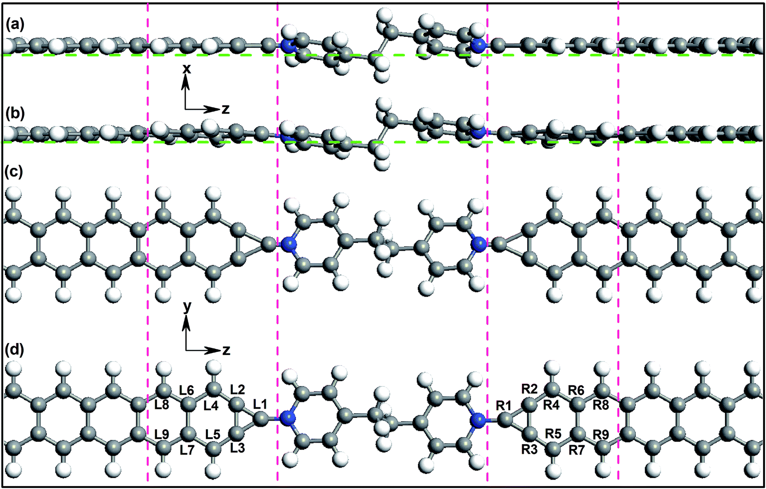
The studied devices composed of pyridine-linked molecules (4,4′-bipyridine, 4,4′-vinylenedipyridine and 4,4′-ethylenedipyridine) are denoted as M1, M2 and M3 respectively, as illustrated in Fig. 1. The electrodes are made of ZGNRs with widths of 4-atoms. The core molecules of devices M1 and M2 are conjugated, while the core molecule of device M3 has a saturated bridge. A carbon atom is adopted as the alligator clip to provide chemical and geometrical stability between the molecule and electrode; it is bonded to a nitrogen atom of the molecule and positioned symmetrically above the center site of the electrodes. To prevent interactions with adjacent images, these devices are modeled within a supercell with more than 10 Å of vacuum space.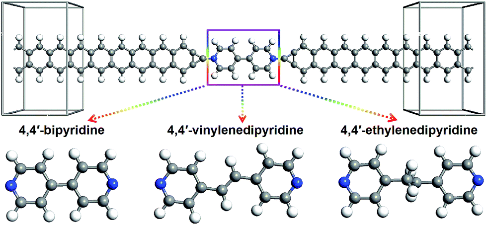 | ||
| Fig. 1 Schematic diagram of the three pyridine-linked single molecular devices, M1, M2 and M3, with narrow zigzag graphene nanoribbon electrodes; the three core molecules are 4,4′-bipyridine, 4,4′-vinylenedipyridine and 4,4′-ethylenedipyridine, respectively. | ||
In this work, the geometric optimizations and the transport calculations are performed by the Atomistix Toolkit (ATK) package, using the first-principles method based on density functional theory (DFT) and non-equilibrium Green's functional theory (NEGF).30–32 The k-point sampling set is 1 × 1 × 100 for the devices. To achieve high-precision calculations, the Perdew–Burke–Ernzerhof (PBE) formulation of the generalized gradient approximation (GGA) is used as the exchange–correlation functional,33 and the double-zeta plus polarization (DZP) basis for all atoms is adopted. Before calculating the electron transport properties, these devices are optimized using the quasi-Newton method until all residual forces on each atom are smaller than 0.05 eV Å−1. The mesh cut-off for the electrostatic potentials is 75 Ha and the temperature in the Fermi function is set as 300 K. The convergence criterion for the total energy is 10−5 via the mixture of the Hamiltonian.
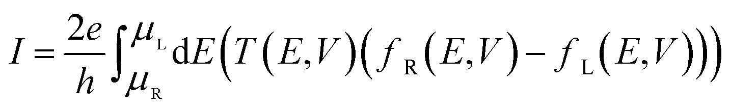
The current through a molecular device is calculated from the Landauer–Büttiker equation34,35
 | (1) |
| T(E,V) = tr[ΓL(E,V)GR(E,V)ΓR(E,V)GA(E,V)] | (2) |
III Results and discussion
Fig. 2a depicts the I–V characteristics of the three devices in a bias region [−1.5 V, 1.5 V]. For all devices, under lower biases, the current varies approximately linearly, displaying approximate ohmic behavior. However, the current changes rapidly with increasing voltage, and shows nonlinear behavior, especially for devices M1 and M2 which contain conjugated molecules. The large current of the device M1 is remarkably coincident with that of the device M2 and a striking low-bias NDR feature appears in both these two devices. This is of particular interest because the NDR effect is indispensable for several electronic components such as the Esaki and resonant tunneling diodes36,37 and the low bias makes the NDR effect more easily implemented.38 In contrast, the current of device M3 is much lower but it displays low-bias NDR with multi-peaks and slight rectification behavior, which is well reflected in Fig. 2b and its inset. Of particular interest is the multi-NDR behavior, as it can be applied to multiple-valued memory, analog-to-digital converters and multiple-valued logics.39 To evaluate the molecular rectification more intuitively, we define the rectification ratio as R(V) = I(+V)/|I(−V)| and this is presented in the inset. It supplies the absolute value of the current through the device M3 as a function of the absolute value of the negative bias, in contrast to the I–V curve under positive biases (see Fig. 2c and d). Initially, the variation of the current under the positive bias is consistent with the current with negative voltage. However, from about 1.15 V, discrepancies begin to arise and meanwhile the rectification ratio increases.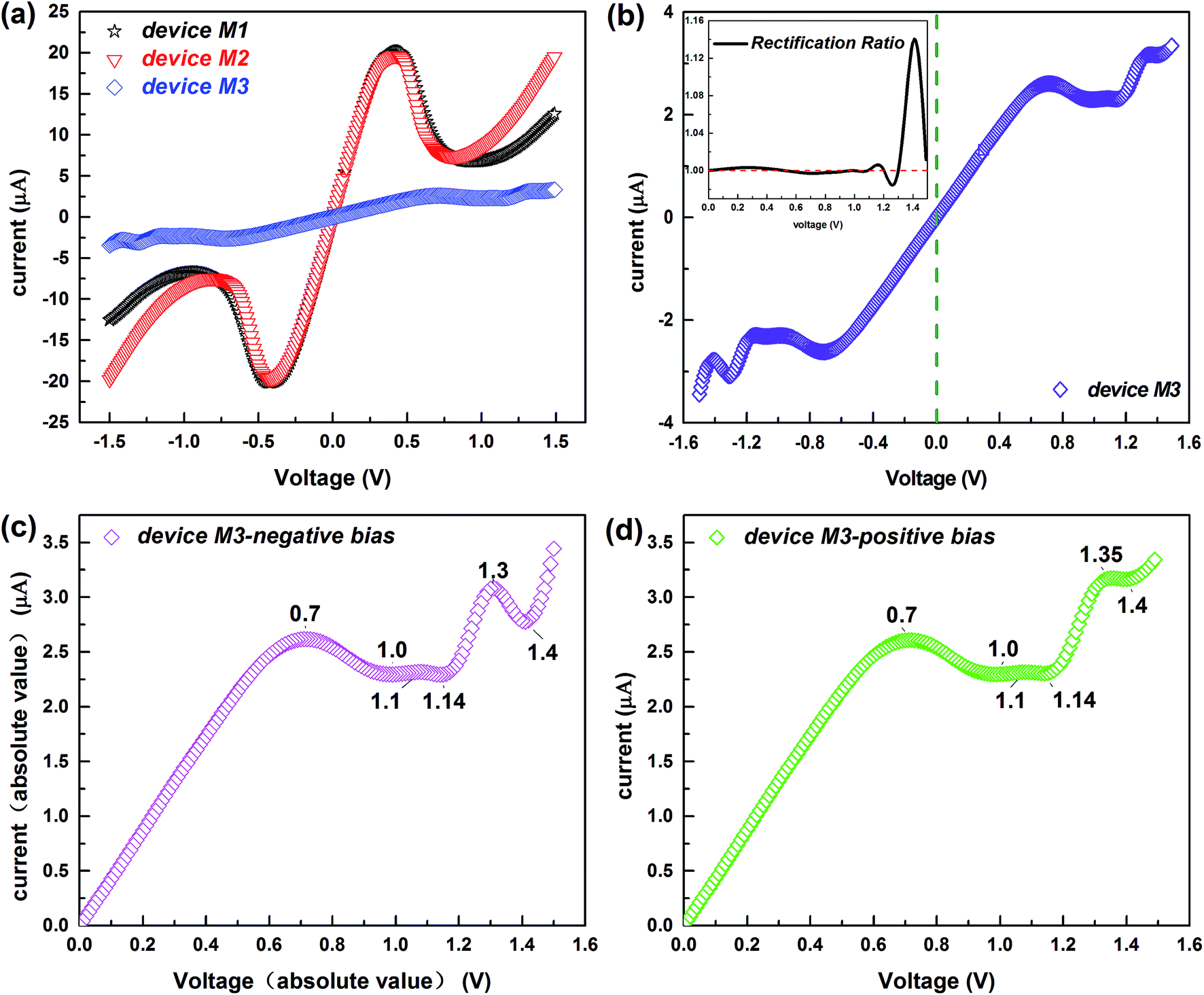 | ||
| Fig. 2 (a) I–V curves of the studied devices in the bias region [−1.5 V, 1.5 V]. (b) I–V curve of the device M3 in the bias region [−1.5 V, 1.5 V]; the inset shows the rectification ratio changing with the voltage. (c) The absolute value of the current through the device M3 as a function of the absolute value of the negative bias. (d) I–V curve of the device M3 under the positive biases. The biases at turning points are marked in (c) and (d). | ||
The analysis of the transmission spectrum at biases may give us clear information about the I–V characteristics, since the current depends on the integral area of the transmission curve running into the bias window from the Landauer–Büttiker formula. Thus, we present the transmission spectra of all studied devices at typical biases in Fig. 3. Because of the symmetry of the I–V curves, the typical biases of devices M1 and M2 focus on the positive voltage range [0, 1.5 V]. We give preference to the region in which the NDR effect is relatively obvious, considering the multi-peak NDR and rectification effect of the device M3. Fig. 2b–d show that the current of the device M3 differs little under low positive and low negative voltages, so we just choose the typical low-positive biases. As the voltage rises, the NDR effect is more apparent at negative biases, so the typical high-negative biases are of more interest. Interestingly, as exhibited in Fig. 3, there are two transmission peaks initially, for devices M1 and M2 which contain conjugated molecules, but only peak I overlaps the bias window contributing to the current. Later, peak I declines gradually, then perishes and meanwhile peak II enters into the bias window devoted to the current. Dissimilarly, only one transmission peak exists for device M3 which is dedicated to the current, whether under positive or negative bias.
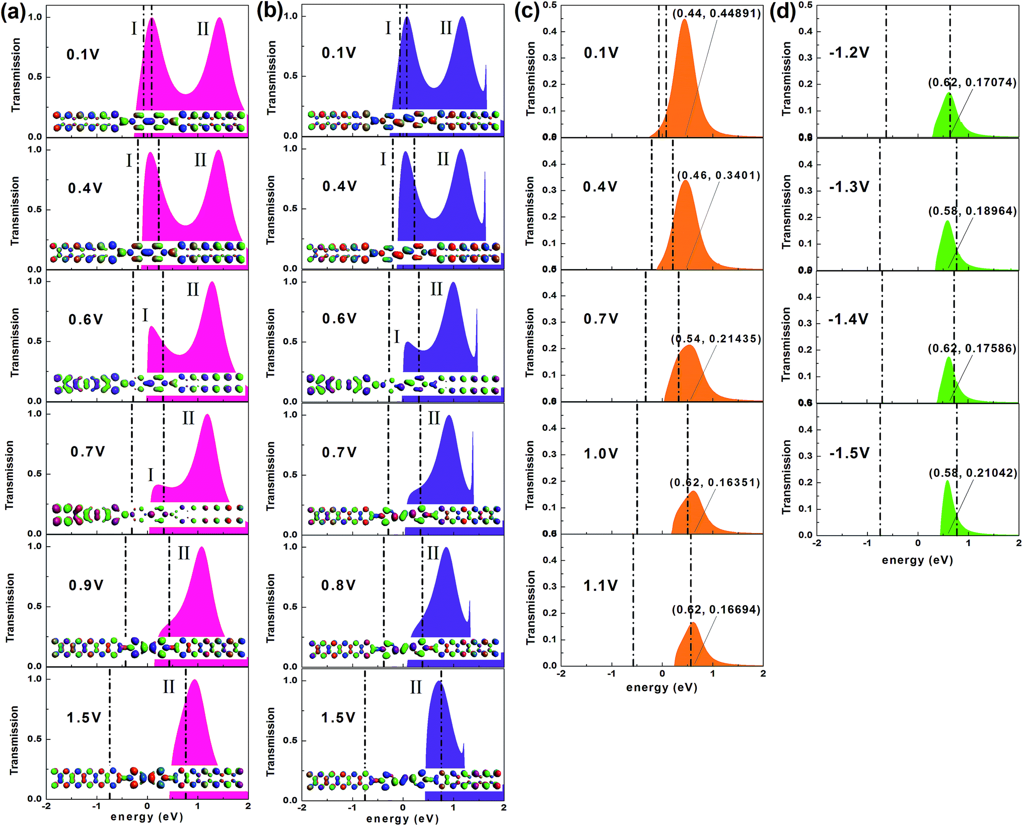 | ||
| Fig. 3 (a and b) Transmission spectra of devices M1 and M2 respectively, at typical biases. The transmission peaks are labeled as I and II. The insets show the transmission eigenstates of the contributing peaks with the same isosurface value at the corresponding biases. (c) Transmission spectra of the device M3 under typical low-positive voltages. (d) Transmission spectra of the device M3 under typical high-negative voltages. Each transmission spectrum of device M3 shows the coordinate value of the transmission peak point. The middle region between the black dotted lines denotes the bias window (BW). | ||
Furthermore, the ribbon widths affect the transport properties. Influenced by the edge shape of the ZGNRs, the width can only be an even number of atoms wide, so we choose four ribbon widths (4, 6, 8, and 10-atoms) to study the performance of the two kinds of devices (4,4′-bipyridine (M1) and 4,4′-ethylenedipyridine (M3) molecules are selected as representatives). The studied device structures and the corresponding transmission spectra are displayed respectively in the sets of Fig. S1 and S2 in the ESI.† For the conjugated devices, the transmission at the Fermi level differs little when the ribbon width is very small (4, 6-atoms wide), although the shape of the curve for the 6-atom wide ribbon is more complex. As the width increases (8, 10-atoms wide), obviously the transmission value at the Fermi level decreases and besides isolated high resonance peaks, small transmission peaks appear close to the Fermi level, which indicates that the edge state contributes greatly to the transport properties of the ZGNRs.40–43 In contrast, for the device with the saturated bridge, more peaks appear in the transmission spectrum when the ribbon width is above 4 atoms. The devices with a narrow electrode (4, 6-atoms wide) show quite weak transmission at the Fermi level but the transmission gets stronger as the width increases (8, 10-atoms wide).
However, for the conjugated device, only the 4-atom wide ZGNR-electrode shows the NDR effect; the currents of the conjugated system using ZGNRs with greater widths all increase with an enhanced bias. At the same bias the current decreases with increasing ribbon width, as shown in Fig. S3.† For the saturated system, only the 4-atom wide ZGNR electrode presents a larger current under positive biases than negative biases although the current through it is lower than those obtained using wider electrodes (see Fig. S4†). Thus the 4-atom wide ZGNR electrodes are mainly investigated.
To further understand the discrepancy in the I–V characteristics and the evolution of the transmission peaks between the two kinds of devices with narrow ZGNR electrodes, firstly we probe into the microscopic origin of the contributing transmission peaks. Such isolated and prominent resonance peaks with a maximum transmission value of unity in the transmission spectra of these devices are associated with resonant electron transport through the discrete energy levels of the molecules.43,44 We can obtain the molecular projected self-consistent Hamiltonian (MPSH) by projecting the self-consistent Hamiltonian onto the Hilbert space spanned by the basis functions of the molecule.45 The eigenstates of MPSH can be considered as molecular orbitals renormalized by the molecule–electrode interaction, which give a visual description of the electronic structure. Through comparing the MPSH states with the transmission eigenstates at zero bias46,47 (see Fig. 4a–c), we find that the HOMO leads to the transmission peak I of both device M1 and device M2. The transmission peak II of device M1 originates from the LUMO+1, while that of device M2 originates from the LUMO. The main peak of the device M3 arises from the HOMO, in particular from the joint of the two pyridine rings.
 | ||
| Fig. 4 (a–c) Transmission eigenstates of the contributing peaks and MPSH states of four frontier orbitals at zero bias for devices M1, M2 and M3. (d) MPSH states of the HOMO and LUMO+1 for the device M1 at four typical biases. (e) MPSH states of the HOMO and LUMO for the device M2 at four typical biases. (f) MPSH states of the HOMO for the device M3 under typical positive and negative biases. | ||
It is generally known that a change in the dominating molecular orbitals correlated with the contributing peaks is crucial to electronic transport,48 because molecular orbitals provide possible transmission channels for electronic tunneling.49 Actually, under an external voltage, these molecular orbitals may undergo changes, including variations in their electronic states and shifts in their positions.49–51 Thus we first show the spatial distribution of the dominant orbitals states related to the contributing transmission peaks for all devices at the selected typical biases (Fig. 4d–f). Obviously, the electronic states of the dominating orbitals for devices M1 and M2 are completely delocalized under various biases, resulting in the large current.46,49,52,53 In contrast, the HOMO state of the device M3 shows gradual localization with the enhancement of the voltage, leading to the lower current of the device M3 in comparison to those of the other devices. Moreover, the states of the dominant orbitals for the device M3 become asymmetric gradually, as the bias increases, and exhibit a high degree of asymmetry at higher biases, in accordance with the variation of the rectification ratio following the voltage change. Noticeably, the electronic states of the HOMO at the positive biases differ greatly from those at the same negative biases. Thus, the rectifying behavior is caused by the gradually increasing and apparent asymmetry of the electronic states belonging to the dominating orbital under the external bias, along with the quite different responses of the dominating orbital to the positive and negative biases.
Actually, this electronic asymmetry results from the asymmetry of the device structure. Interestingly, such asymmetry is caused by the interaction between the non-planar molecule with the saturated bridge and one-dimensional narrow ZGNR electrodes. Here, during the optimization of the device structure, the molecule itself does not change; only the atoms at the contact of the molecule and each electrode may change. Fig. 5 shows the unoptimized and optimized structures of the device M3; the atoms at the contact places that change substantially have been labeled. Obviously, the atoms L1–L9 are not in the same plane (yz) as the atoms R1–R9. Such changes can be quantified by describing the variation of the coordinates of these atoms. To confirm the asymmetry of the contact, the x-coordinates and y-coordinates of the atoms at each contact are presented in Table 1.
 | ||
| Fig. 5 (a and b) Unoptimized and optimized structures of the device M3 seen in the xz plane. (c and d) Unoptimized and optimized structures of device M3 seen in the yz plane. Each green dashed line is along the direction of the electrode (i.e. z direction). The atoms at two contact places are labeled and framed in pink-dashed lines. | ||
| Atomic number | Coordinate | Atomic number | Coordinate | ||
|---|---|---|---|---|---|
| x | y | x | y | ||
| L1 | 5.01 | 6.44 | R1 | 4.99 | 6.40 |
| L2 | 5.12 | 7.15 | R2 | 5.07 | 7.13 |
| L3 | 4.93 | 7.71 | R3 | 4.87 | 5.69 |
| L4 | 5.22 | 7.90 | R4 | 5.15 | 7.89 |
| L5 | 4.86 | 4.95 | R5 | 4.77 | 4.94 |
| L6 | 5.11 | 7.16 | R6 | 5.03 | 7.15 |
| L7 | 4.97 | 5.68 | R7 | 4.88 | 5.68 |
| L8 | 5.14 | 7.83 | R8 | 5.08 | 7.83 |
| L9 | 4.93 | 5.01 | R9 | 4.85 | 5.01 |
Here, for the symmetrical contact of the molecule and the ZGNR electrode (along the z axis), the corresponding x-coordinates and y-coordinates of the atoms at the two contacts should be the same, which is evidently not the case for the optimized device M3 (Table 1). On the whole, the differences in the y-coordinates are small, especially for the atoms L4–L9 and R4–R9, while the differences in the x-coordinates are relatively big. This shows intuitively the asymmetry of the contact. Such asymmetry caused by deformation only exists in the connection between this kind of non-planar molecule with a saturated bridge and a one-dimensional narrow ZGNR electrode. To maintain the stability of the device structure, the atoms at the join deform so that they are no longer in the plane of the narrow ZGNR electrode, when the narrow ZGNR electrode contacts a molecule whose two rings are not in the one plane. Moreover, the saturated bridge bonding the two rings is not perpendicular to the plane of the narrow ZGNR electrode (note that the left electrode and the right electrode are kept in one plane), resulting in the asymmetrical deformation of the contact on both sides.
The rectifying behavior is mainly attributed to this specific M3 core molecule and narrow ZGNR electrodes (it does not appear either for the devices M1 and M2 with identical electrodes as shown in Fig. 2a, or for the devices with M3 connected to Au and Ag electrodes, as presented in Fig. S5 in the ESI†). It is not induced by deliberately changing the configuration through substituting the electrode material on one side54 or by adopting two different molecule–electrode coupling modes on the two sides.55,56
Next, we come to the profound explanation of the inner mechanism for the I–V variation trend, especially the revelation about the root cause of the NDR effect. The occurrence of the NDR phenomenon can be understood from the evolution of the quantum conductance.57 For these devices, a decrease in the current is accompanied by a reduction in the quantum conductance, as Fig. 6a and b and S6† show. Furthermore, for the conjugated systems, which display a transition from two transmission peaks to one, the electronic states of the dominating orbitals remain unchanged under the applied bias. Therefore, we concentrate on the variation in position of these governing orbitals (see Fig. 6c and d).
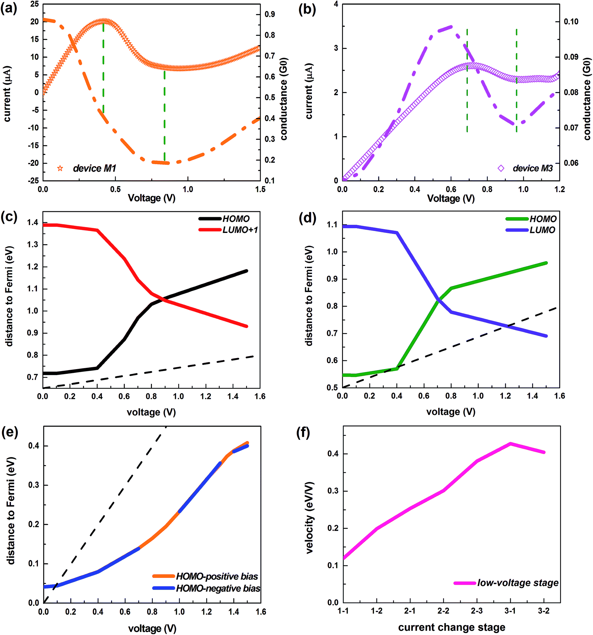 | ||
| Fig. 6 (a) Current and quantum conductance of the device M1 under the bias [0 V, 1.5 V]. (b) Current and quantum conductance of the device M3 under the bias [0 V, 1.2 V]. In (a and b), the segment of the I–V curve inside the dashed line denotes the stage of declining current. (c and d) Distance between the Fermi level and the dominant orbitals as a function of the positive biases for devices M1 and M2, respectively. (e) The function of the distance between the Fermi level and the dominant orbitals under the positive and negative voltages depending on the absolute voltage, for the device M3. The dotted lines indicate the line of the bias window. (f) The velocity of the HOMO orbital away from the Fermi level during the low-voltage stage for the device M3. Stages 1-1, 1-2 represent the initial increasing stages of the current; stages 2-1, 2-2, 2-3 signify the declining stages of the current; stages 3-1, 3-2 express the current recovery stages. | ||
For the device M1, initially, the positions of the HOMO and the LUMO+1 show no significant change, but the HOMO lies much closer to the Fermi level, indicating that the HOMO is the main contributor to the transmission.58 Thus the integral area of the HOMO-controlled transmission peak I gains greater access to the bias window, as the voltage rise is accompanied by the enlargement of the bias window, causing the enormously enhanced current. After this stage, the HOMO starts to withdraw from the Fermi level rapidly, and further triggers a reductive influence on the current (this can be seen in the localized transmission eigenstates of peak I at 0.6 V and 0.7 V, as described in the insets of Fig. 3a), bringing about the decrease of the current with the augment of the bias, i.e. the NDR effect. In the meantime, the LUMO+1 swiftly approaches the Fermi level and starts to impact the transmission. At about 0.9 V, when the two orbitals are the same distance to the Fermi level, the LUMO+1 supersedes the HOMO that initially occupies a leading position in the electron transport, resulting in the complete disappearance of the HOMO-leading transmission peak I. Subsequently, the HOMO moves away from the Fermi level while the LUMO+1 continues toward the Fermi level, with the result that a greater amount of the integral area of transmission peak II induced by the LUMO+1 gets into the bias window. Furthermore, the transmission peak II exhibits stronger transmission states, as demonstrated in the inset at 1.5 V of Fig. 3a. Therefore, the current rises again and the NDR behavior disappears.
It can be concluded that the aforementioned explanation applies equally to the other conjugated device M2 which displays a similar evolution of transmission peaks and current under the external bias (compare Fig. 3a with 3b and Fig. 6c with 6d).
For the device M3 with its saturated bridge, there is always one transmission peak under the applied voltages. As displayed in Fig. 6e, the dominant orbital (the HOMO) moves away from the Fermi level, whether under the positive bias or not, but it mostly remains within the bias window. Thus, it always plays an irreplaceable role in the transmission. At the low-positive biases, the transmission peak point steps down due to the gradual localization of the HOMO states from the initial stage of increasing current to the stage of declining current (i.e. [0.1 V, 1.0 V]), as shown in Fig. 4f. The current still rises in the bias region [0.1 V, 0.7 V], mainly because the movement of the HOMO away from the Fermi level gets slower (see Fig. 6f), which slows the speed of the transmission peak away from the Fermi level, and at the same time, the bias window is enlarged. Here, the moving speed is defined as the ratio of the moving energy values to the corresponding voltage changes. Then the occurrence of the NDR performance in the bias range [0.7 V, 1.0 V] originates from the combined effect of both the localized state of the dominant orbital and the higher velocity of the leading orbital away from the Fermi level. Beyond 1.0 V, the localization of the HOMO is no longer strengthened (see Fig. 4f), leading to the ascent of the summit of the transmission peak, and the velocity of this orbital begins to drop so that the transmission peak does not move away from the Fermi level any longer. As a consequence, the current rises again.
At the high-negative biases, the transmission peak height and the distance between the peak and the Fermi level keep pace with the current, as illustrated in Fig. 3d. Specifically, the peak height is elevated and the peak moves closer to the Fermi level when the current increases. And the peak height is reduced and the peak moves far away from the Fermi level when the current decreases. Actually, the shift of the transmission peak exceeds the increasing of the chemical potential window leading to the decreasing of the total transmission coefficient; thus, the corresponding current decreases and the NDR behavior appears.59
In addition, when the molecule connects to the electrode, a contact potential is generated, which affects the transport properties. We place the three molecules between 4 × 4 Au (111) and Ag (111) electrodes to investigate the influence of the contact potential. Similar to the connection mode of the ZGNR electrode, a gold (or silver) atom is adopted as the alligator clip to provide chemical and geometrical stability between the molecule and electrode, which is bonded to a nitrogen atom of the molecule and positioned symmetrically above the center site of the electrode. Fig. 7 shows isosurface plots of the electrostatic difference potentials for these devices. Obviously, when the pyridine molecule connects to the electrodes made from different materials, the corresponding devices present different electrostatic potential distributions.
 | ||
| Fig. 7 (a–c) Isosurface plots of the electrostatic difference potentials for 4,4′-bipyridine-based devices with 4-atom ZGNR, Au and Ag electrodes, respectively. (d–f) Isosurface plots of the electrostatic difference potentials for 4,4′-vinylenedipyridine-based devices with 4-atom ZGNR, Au and Ag electrodes, respectively. (g–i) Isosurface plots of the electrostatic difference potentials for 4,4′-ethylenedipyridine-based devices with 4-atom ZGNR, Au and Ag electrodes, respectively. | ||
From Fig. 7b, c, e, f, h and i, the accumulation of the electrostatic potential can be observed clearly in the molecular region of the metal-based devices due to the larger work function60 of the pyridine molecule, and each joint atom displays a depletion of the electrostatic potential. The contact surface of the Au electrode shows an accumulation of the electrostatic potential, which results in the larger current of Au-based devices (see Fig. S5†). Dramatically, an accumulation of the electrostatic potential can be found in the ZGNR electrode region and most regions of the molecule, which leads to the ZGNR-based devices displaying the largest currents (see Fig. S5†). Moreover, the more complex areas surrounding the molecule of device M3 exhibit depletion of the electrostatic potential, which facilitates the unique I–V characteristics of device M3.
Notably, the distinctive I–V characteristics (including the robust NDR effect) shown in the two conjugated devices (M1 and M2) appear neither for the device M3 (with the same electrodes and another kind of pyridine-linked core molecule), nor for the devices composed of the same core molecule with metal (Au, Ag) electrodes, which is reflected in their I–V curves (see Fig. S5a and b†). This indicates that the excellent performances are determined by the conjugated core molecules and ZGNR electrodes together. Similarly, the specific I–V features demonstrated by the device M3 (containing the multistage NDR effect together with the slight rectification effect) do not occur simultaneously in devices M1 or M2 (with two conjugated molecules sandwiched between the same electrodes), or in the devices with M3 connected to Au or Ag electrodes (the correlative I–V curves are illustrated in Fig. S5c†). Thus the specific I–V behavior essentially depends on both the type of pyridine-based molecule and the narrow ZGNR electrodes. Thus it can be seen that information on both the core molecule and the electrodes must be taken into serious consideration in the design of molecular devices.
IV Conclusion
In summary, we have thoroughly investigated the non-equilibrium electron transport properties (I–V characteristics) of three pyridine-terminated systems using the same narrow ZGNR electrodes and two kinds of core molecules, by DFT and NEGF techniques. The conjugated devices show (i) the conversion of two transmission peaks to one with increased voltage, which can be attributed to the novation of the dominant orbital, and (ii) an obvious NDR effect rooted in the escape of the initial dominant orbital away from the Fermi level. Interestingly, the device based on a saturated bridge displays much lower current than the conjugated devices which originates from gradual localization of the electronic states of the dominating orbital, and slight rectifying behavior caused by the quite different responses of the dominating orbital to the positive and negative biases along with the obvious asymmetry of its electronic states. In addition, the multi-NDR behavior occurs in this device with only one transmission peak and it has a different internal mechanism for its NDR behavior: the low-bias NDR performance is derived from the combined effect of the localized electronic state and a higher velocity away from the Fermi level of the dominant orbital. The widths of the ZGNR electrodes also influence the transport properties. These physical effects and the relevant basic inner mechanisms have extensive potential application in the development of high-speed logic devices,39,61 because of the relevant basic inner mechanisms.Conflicts of interest
There are no conflicts to declare.Acknowledgements
The authors would like to acknowledge the support from the National Natural Science Foundation of China (Grant No. 51671114). This work is also supported by Special Funding in the Project of the Taishan Scholar Construction Engineering.References
- I.-W. Lyo and P. Avouris, Science, 1989, 245, 1369 CAS.
- M. M. Kaneda, K. S. Messer, N. Ralainirina, H. Li, C. J. Leem, S. Gorjestani, G. Woo, A. V. Nguyen, C. C. Figueiredo and P. Foubert, Nature, 2017, 542, 124 CrossRef CAS PubMed.
- C. Guo, K. Wang, E. Zerah-Harush, J. Hamill, B. Wang, Y. Dubi and B. Xu, Nat. Chem., 2016, 8, 484–490 CrossRef CAS PubMed.
- T. Ryu, Y. Lansac and Y. H. Jang, Nano Lett., 2017, 17(7), 4061–4066 CrossRef CAS PubMed.
- X.-C. Li, H. Sirringhaus, F. Garnier, A. B. Holmes, S. C. Moratti, N. Feeder, W. Clegg, S. J. Teat and R. H. Friend, J. Am. Chem. Soc., 1998, 120, 2206–2207 CrossRef CAS.
- M. M. Alsaif, A. F. Chrimes, T. Daeneke, S. Balendhran, D. O. Bellisario, Y. Son, M. R. Field, W. Zhang, H. Nili and E. P. Nguyen, Adv. Funct. Mater., 2016, 26, 91–100 CrossRef CAS.
- H. Cho, S.-H. Jeong, M.-H. Park, Y.-H. Kim, C. Wolf, C.-L. Lee, J. H. Heo, A. Sadhanala, N. Myoung and S. Yoo, Science, 2015, 350, 1222–1225 CrossRef CAS PubMed.
- Z.-K. Tan, R. S. Moghaddam, M. L. Lai, P. Docampo, R. Higler, F. Deschler, M. Price, A. Sadhanala, L. M. Pazos and D. Credgington, Nat. Nanotechnol., 2014, 9, 687–692 CrossRef CAS PubMed.
- J. Xiang, T.-K. Wang, Q. Zhao, W. Huang, C.-L. Ho and W.-Y. Wong, J. Mater. Chem. C, 2016, 4, 921–928 RSC.
- S. Liu, N. Lu, X. Zhao, H. Xu, W. Banerjee, H. Lv, S. Long, Q. Li, Q. Liu and M. Liu, Adv. Mater., 2016, 28, 10809 CrossRef CAS.
- J. Chen, M. Reed, A. Rawlett and J. Tour, Science, 1999, 286, 1550–1552 CrossRef CAS PubMed.
- I. V. Antonova, I. I. Kurkina, N. A. Nebogatikova, A. I. Komonov and S. A. Smagulova, Nanotechnology, 2017, 28, 074001 CrossRef PubMed.
- G. W. Burg, N. Prasad, B. Fallahazad, A. Valsaraj, K. Kim, T. Taniguchi, K. Watanabe, Q. Wang, M. J. Kim and L. F. Register, Nano Lett., 2017, 17(6), 3919–3925 CrossRef CAS PubMed.
- J. Li and Q. Zhang, Carbon, 2005, 43, 667–670 CrossRef CAS.
- P. Routh, R. K. Layek and A. K. Nandi, Carbon, 2012, 50, 3422–3434 CrossRef CAS.
- M. S. Johnson, L. Wickramasinghe, C. Verani and R. M. Metzger, J. Phys. Chem. C, 2016, 120, 10578–10583 CAS.
- J. Li, Z. Zhang, M. Qiu, C. Yuan, X. Deng, Z. Fan, G. Tang and B. Liang, Carbon, 2014, 80, 575–582 CrossRef CAS.
- B. Xu and N. J. Tao, Science, 2003, 301, 1221–1223 CrossRef CAS PubMed.
- S. Y. Quek, M. Kamenetska, M. L. Steigerwald, H. J. Choi, S. G. Louie, M. S. Hybertsen, J. Neaton and L. Venkataraman, Nat. Nanotechnol., 2009, 4, 230–234 CrossRef CAS PubMed.
- M. Kamenetska, S. Y. Quek, A. Whalley, M. Steigerwald, H. Choi, S. G. Louie, C. Nuckolls, M. Hybertsen, J. Neaton and L. Venkataraman, J. Am. Chem. Soc., 2010, 132, 6817–6821 CrossRef CAS PubMed.
- Á. J. Pérez-Jiménez, J. Phys. Chem. B, 2005, 109, 10052–10060 CrossRef PubMed.
- R. Stadler and K. W. Jacobsen, Phys. Rev. B: Condens. Matter Mater. Phys., 2006, 74, 161405 CrossRef.
- X. Shi, X. Zheng, Z. Dai, Y. Wang and Z. Zeng, J. Phys. Chem. B, 2005, 109, 3334–3339 CrossRef CAS PubMed.
- O. Adak, R. Korytar, A. Y. Joe, F. Evers and L. Venkataraman, Nano Lett., 2015, 15, 3716–3722 CrossRef CAS PubMed.
- J. Rauba, M. Strange and K. S. Thygesen, Phys. Rev. B: Condens. Matter Mater. Phys., 2008, 78, 165116 CrossRef.
- A. K. Geim and K. S. Novoselov, Nat. Mater., 2007, 6, 183–191 CrossRef CAS PubMed.
- L. Ponomarenko, F. Schedin, M. Katsnelson, R. Yang, E. Hill, K. Novoselov and A. Geim, Science, 2008, 320, 356–358 CrossRef CAS PubMed.
- B. Standley, W. Bao, H. Zhang, J. Bruck, C. N. Lau and M. Bockrath, Nano Lett., 2008, 8, 3345–3349 CrossRef CAS PubMed.
- J. Li, T. Li, Y. Zhou, W. Wu, L. Zhang and H. Li, Phys. Chem. Chem. Phys., 2016, 18, 28217–28226 RSC.
- M. Brandbyge, J.-L. Mozos, P. Ordejón, J. Taylor and K. Stokbro, Phys. Rev. B: Condens. Matter Mater. Phys., 2002, 65, 165401 CrossRef.
- J. M. Soler, E. Artacho, J. D. Gale, A. García, J. Junquera, P. Ordejón and D. Sánchez-Portal, J. Phys.: Condens. Matter, 2002, 14, 2745 CrossRef CAS.
- J. Taylor, H. Guo and J. Wang, Phys. Rev. B: Condens. Matter Mater. Phys., 2001, 63, 245407 CrossRef.
- J. P. Perdew and A. Zunger, Phys. Rev. B: Condens. Matter Mater. Phys., 1981, 23, 5048 CrossRef CAS.
- R. Landauer, Philos. Mag., 1970, 21, 863–867 CrossRef CAS.
- S. Datta, Electronic transport in mesoscopic systems, Cambridge University Press, 1997 Search PubMed.
- S. M. Sze and K. K. Ng, Physics of semiconductor devices, John Wiley & Sons, 2006 Search PubMed.
- R. H. Mathews, J. P. Sage, T. G. Sollner, S. D. Calawa, C.-L. Chen, L. J. Mahoney, P. A. Maki and K. M. Molvar, Proc. IEEE, 1999, 87, 596–605 CrossRef.
- K. H. Khoo, J. Neaton, Y. W. Son, M. L. Cohen and S. G. Louie, Nano Lett., 2008, 8, 2900–2905 CrossRef CAS PubMed.
- H. Inokawa, A. Fujiwara and Y. Takahashi, Appl. Phys. Lett., 2001, 79, 3618–3620 CrossRef CAS.
- L. Shen, M. Zeng, S.-W. Yang, C. Zhang, X. Wang and Y. Feng, J. Am. Chem. Soc., 2010, 132, 11481–11486 CrossRef CAS PubMed.
- S. J. van der Molen and P. Liljeroth, J. Phys.: Condens. Matter, 2010, 22, 133001 CrossRef PubMed.
- C. Motta, M. Trioni, G. Brivio and K. Sebastian, Phys. Rev. B: Condens. Matter Mater. Phys., 2011, 84, 113408 CrossRef.
- I. A. Pshenichnyuk, P. B. Coto, S. Leitherer and M. Thoss, J. Phys. Chem. Lett., 2013, 4, 809–814 CrossRef CAS PubMed.
- J. C. Dong, H. Li, F. W. Sun and Y. F. Li, J. Phys. Chem. C, 2012, 116, 6762–6769 CAS.
- Z. Li and D. S. Kosov, J. Phys. Chem. B, 2006, 110, 19116–19120 CrossRef CAS PubMed.
- K. Stokbro, J. Taylor, M. Brandbyge, J.-L. Mozos and P. Ordejon, Comput. Mater. Sci., 2003, 27, 151–160 CrossRef CAS.
- K. S. Thygesen and K. W. Jacobsen, Chem. Phys., 2005, 319, 111–125 CrossRef CAS.
- J. Li, S.-C. Dong, A. Opitz, L. Liao and N. Koch, J. Mater. Chem. C, 2017, 5, 6989–6996 RSC.
- Q. Bao, Z. Lu, J. Li, K. P. Loh and C. M. Li, J. Phys. Chem. C, 2009, 113, 12530–12537 CAS.
- Z. Zhang, C. Guo, D. J. Kwong, J. Li, X. Deng and Z. Fan, Adv. Funct. Mater., 2013, 23, 2765–2774 CrossRef CAS.
- D. Nozaki, A. Santana-Bonilla, A. Dianat, R. Gutierrez and G. Cuniberti, J. Phys. Chem. Lett., 2015, 6, 3950–3955 CrossRef CAS PubMed.
- A. Staykov, D. Nozaki and K. Yoshizawa, J. Phys. Chem. C, 2007, 111, 11699–11705 CAS.
- Z.-Q. Fan and K.-Q. Chen, Appl. Phys. Lett., 2010, 96, 053509 CrossRef.
- J. Pan, Z. Zhang, K. Ding, X. Deng and C. Guo, Appl. Phys. Lett., 2011, 98, 092102 CrossRef.
- J. Zhao, C. Yu, N. Wang and H. Liu, J. Phys. Chem. C, 2010, 114, 4135–4141 CAS.
- C. Guo, Z. Zhang, G. Kwong, J. Pan, X. Deng and J. Zhang, J. Phys. Chem. C, 2012, 116, 12900–12905 CAS.
- J. Zhao and H. Zeng, Phys. Chem. Chem. Phys., 2016, 18, 9809–9815 RSC.
- K. Yoshizawa, T. Tada and A. Staykov, J. Am. Chem. Soc., 2008, 130, 9406–9413 CrossRef CAS PubMed.
- Z. Fan, Z. Zhang, X. Deng, G. Tang, C. Yang, L. Sun and H. Zhu, Carbon, 2016, 98, 179–186 CrossRef CAS.
- J. B. Pan, Z. H. Zhang, K. H. Ding, X. Q. Deng and C. Guo, Appl. Phys. Lett., 2011, 98, 092102 CrossRef.
- A. Salomon, R. Arad-Yellin, A. Shanzer, A. Karton and D. Cahen, J. Am. Chem. Soc., 2004, 126, 11648–11657 CrossRef CAS PubMed.
Footnote |
| † Electronic supplementary information (ESI) available. See DOI: 10.1039/c7ra09552j |
| This journal is © The Royal Society of Chemistry 2017 |