DOI:
10.1039/C7RA09484A
(Paper)
RSC Adv., 2017,
7, 50571-50577
30-Fold efficiency enhancement achieved in the perovskite light-emitting diodes†
Received
27th August 2017
, Accepted 20th October 2017
First published on 30th October 2017
1 Introduction
Since the first room-temperature halide perovskite light-emitting diode (PeLEDs) was demonstrated by Friend's group in 2014,1 perovskite materials have been considered as promising light emitters and have been paid enormous attraction by worldwide research groups.2–9 According to their pioneer investigation, it was proved that all-inorganic cesium lead halide perovskite emitters of a common composition CsPbX3 (X = Cl, Br, and I or mixed halide) have a better thermal stability (up to their melting temperature of about 500 °C) than the organometal ones.2 And it should be noted that CsPbBr3 is thermally stable up to 250 °C in air formed via solution process.3 Moreover, it is found that the CsPbBr3 can provide a high charge-carrier mobility (∼1000 cm2 V−1 s−1),5 and low trap density,6 high photoluminescence (PL) quantum yield (up to 90% in solution),7,8 and spectra with very high color purity (full width at half maximum, FWHM, ∼20 nm) stimulated at room temperature.9 These attractive thermal and optoelectronic properties of CsPbBr3 are beneficial to PeLEDs.
One of key factors to achieve high electroluminescent (EL) performance in all-inorganic PeLEDs is to obtain high quality flat and uniform perovskite films with high coverage, and small grains.10–21 There are two main ways to fabricate all-inorganic cesium lead halide perovskite films.11–23 The first way is to prepare perovskite quantum dot films from dispersion of pre-synthesized perovskite colloidal nanocrystals.12–18 The Kovalenko's method is involved to form the pre-synthesized perovskite colloidal nanocrystals, which needs the protection of N2 and a high reaction temperature ranged from 100 °C to 200 °C.24,25 The other way is to obtain perovskite films directly from a perovskite precursor solution.19–22 The perovskite precursor solution is gained by dissolving both CsBr and PbBr2 in organic solvent such as dimethyl sulphoxide (DMSO), which is more simple than the Kovalenko's method. Moreover, the film deposited via the first way is relatively poor in film coverage due to the insolubility of the perovskite nanoparticle in toluene, and relatively poor conductivity caused by commonly used insulated long-chain surface ligands (such as oleic acid and oleylamine).14 Thus, the second way is used in this work.
Although the post-treatment processes to the all-inorganic perovskite films deposited via the above two methods are different, in most cases, researchers are used to annealing the perovskite films in order to make the films crystallize and the organic solvent volatilize faster to obtain high quality perovskite films with good coverage.13,16,19,20 To date, for the annealed films formed via the first way, the best reported neat CsPbBr3 quantum dots (QDs) PeLEDs are fabricated from films annealed at 90 °C for 5 min in glove box,13 showing a maximum luminance of 1698 cd m−2 for equimolar PbBr2–CsBr ones, and 3853 cd m−2 for CsBr-rich ones (PbBr2![[thin space (1/6-em)]](https://www.rsc.org/images/entities/char_2009.gif) :CsBr = 1:2). While for the films without annealing formed via the first way, the best reported one is just dried in air for 10 min2, exhibiting maximum luminance of 2335 cd m−2 for the equimolar PbBr2–CsBr ones. However, for the annealed film via the second way, the best reported neat equimolar (CsBr-rich) CsPbBr3 PeLEDs are fabricated from films annealed at 70 °C for 5 min (70 °C for 10 min) in glove box,20,21 showing a maximum luminance of 666 cd m−2 (4800 cd m−2). To improve the luminance, Wei et al.22 developed the third way by firstly obtaining CsPbBr3 powder via adding CsBr aqueous solution dropwise to the PbBr2–HBr solution, and secondly dissolving the as-prepared CsPbBr3 powder in DMSO, and finally depositing by one-step spin-coating, and obtaining a highest maximum luminance of 7276 cd m−2 for CsBr-rich ones (PbBr2:CsBr = 1:1.4). However, the post-treatment process of the CsPbBr3 film is not mentioned in their report and the preparation of the perovskite precursor solution is complicated.
:CsBr = 1:2). While for the films without annealing formed via the first way, the best reported one is just dried in air for 10 min2, exhibiting maximum luminance of 2335 cd m−2 for the equimolar PbBr2–CsBr ones. However, for the annealed film via the second way, the best reported neat equimolar (CsBr-rich) CsPbBr3 PeLEDs are fabricated from films annealed at 70 °C for 5 min (70 °C for 10 min) in glove box,20,21 showing a maximum luminance of 666 cd m−2 (4800 cd m−2). To improve the luminance, Wei et al.22 developed the third way by firstly obtaining CsPbBr3 powder via adding CsBr aqueous solution dropwise to the PbBr2–HBr solution, and secondly dissolving the as-prepared CsPbBr3 powder in DMSO, and finally depositing by one-step spin-coating, and obtaining a highest maximum luminance of 7276 cd m−2 for CsBr-rich ones (PbBr2:CsBr = 1:1.4). However, the post-treatment process of the CsPbBr3 film is not mentioned in their report and the preparation of the perovskite precursor solution is complicated.
In this paper, we found that the method of pumping away the solvent may be a better choice to make the solvent volatilize quickly and get high quality neat all-inorganic cesium lead halide perovskite CsPbBr3 films than the method employing annealing process after pumping away process. The PeLEDs with neat CsPbBr3 film gained by only pumping away method after one-step spin-coating, achieve maximum luminances of 3285 cd m−2 and 5046 cd m−2, maximum current efficiencies of 1.13 cd A−1 and 3.25 cd A−1, maximum external quantum efficiency (EQE) of 0.29% and 0.85% from the equimolar PbBr2–CsBr and CsBr-rich (PbBr2:CsBr = 1:1.2) precursor solutions, respectively, which is among the best results based on neat CsPbBr3 PeLEDs reported so far. Our results offer a facile method to achieve highly efficient PeLEDs by just pumping away after one-step spin-coating at room temperature.
2 Experimental methods
2.1 Material and perovskite CsPbBr3 precursor
Poly(3,4-ethylenedioxythiophene):poly(p-styrene sulfonate) (PEDOT:PSS, Clevios AI 4083) was bought from Heraeus (Germany). The 2,2′,2′′-(1,3,5-benzinetriyl)-tris(1-phenyl-1-H-benzimidazole) (TPBi), 8-hydroxyquinolinato lithium (Liq), and aluminum (Al) were bought from Suzhou Fangsheng Photoelectricity Shares Co, Ltd and their purity are larger than 99%. The perovskite CsPbBr3 precursor solution is obtained by dissolving both PbBr2 and CsBr (Xi'an Polymer Light Technology Corp., >99.99%) with molar ratios of 1:1 in DMSO (Alfa-Aesar, >99.99%) solvent with a concentration of 10 wt% under constant stirring larger than 12 hours.
2.2 Device fabrication
The pre-treated ITO-coated glass substrates, with a sheet resistance of ∼15 Ω sq−1, were sequentially pre-cleaned by acetone, ethanol, and deionized water and dried by oven. After ultraviolet ozone treatment for 5 min, PEDOT:PSS was spin-coated on the ITO surface at 4500 rpm for 40 s and then annealed at 120 °C for 20 min. Then, the substrates were transferred into a nitrogen-filled glove box. Next, the CsPbBr3 film was formed on the PEDOT:PSS by one-step spin-coating from CsPbBr3 precursor solution at 4000 rpm for 60 s with different post-treatment processes. And then, TPBi (65 nm), Liq (2.5 nm), and Al (120 nm) cathode were evaporated on top of CsPbBr3 perovskite film by utilizing a LN-1103SC vacuum thermal depositing system from Shenyang Vacuum Technology Research Institute, where TPBi, Liq/Al are used as an electron transport layer and a bilayer cathode, respectively. The active area of each device was 2 × 3 mm2 which is defined through a shadow mask. All devices were sealed with glass covers in glove box under the protection of N2.
2.3 Measurements and characterization
The top-view and cross-section images were taken with a scanning electron microscopy (SEM) system (JEOL, JSM-7100F). The absorption, PL spectra and time-resolved PL spectra were obtained by UV-Vis spectrophotometer (Shimadzu UV-2600) and fluorescence spectrometer (Folurolog 3), respectively. The atomic force microscope (AFM) images and XRD pattern were obtained by Cypher AFM (Cypher S) and X-ray diffractometer (XRD, TD-3500), respectively. The EL performance and stability of PeLEDs were recorded with a LED testing system including Keithley 2400, calculated Si photodiode (Photoelectric Instrument Factory of Beijing Normal University, ST-86LA), and Photo Research SpectraScan photometer (PR 670).
3 Results and discussion
3.1 Film preparation and surface morphology
The modified and reference neat CsPbBr3 films are obtained by one-step spin-coating from 10 wt% CsPbBr3 in DMSO solution (shown in Fig. 1a and b). The modified CsPbBr3 film is acquired without annealing but only pumping away (Fig. 1c), while the reference CsPbBr3 film is annealed at 70 °C for 5 min after pumping away (the top-view SEM images for the optimization of annealing condition can be found in ESI Fig. S1†). And the pumping away is a method to get CsPbBr3 perovskite film by pumping the solvent component of the precursor film in the transfer chamber of the glove box for 20 min at room temperature after the spin-coating process as shown in Fig. 1c. The pumping away system is comprised of a transfer chamber belonging to a glove box and attached by a mechanical pump. When the mechanical pump is open, the solvent of the precursor film will be pumped away. From the top view SEM images of the neat CsPbBr3 films, it can be found that the coverage of the modified film (Fig. 1d) is improved to 91.1% compared to the reference film (Fig. 1e) of 76.3% (estimated from SEM images by using ImageJ software), and the average grain size is reduced to ∼100 nm compared to that of the reference film of ∼110 nm. Higher coverage and smaller grains suggest that better EL performance can be achieved in the modified film based PeLEDs. In Fig. 1f, similar absorption spectra shapes are demonstrated in both modified and reference neat CsPbBr3 films with absorption band edges of 539 nm and 542 nm, respectively. From the PL spectra in Fig. 1f, it suggests that the both modified and reference neat CsPbBr3 films have the same emission peaks (520 nm) and same FWHM (∼18 nm). However, the modified neat CsPbBr3 film exhibits remarkably higher PL intensity compared to the reference neat CsPbBr3 film excited with equal light intensity at 365 nm (shown in the inset of Fig. 1f). Since the EL efficiency of PeLEDs is proportional to the PL intensity of perovskite, the improvement of PL properties in modified neat CsPbBr3 thin films with only pumping away will be expected to improve the EL efficiency in the modified neat CsPbBr3 thin films based PeLEDs.19
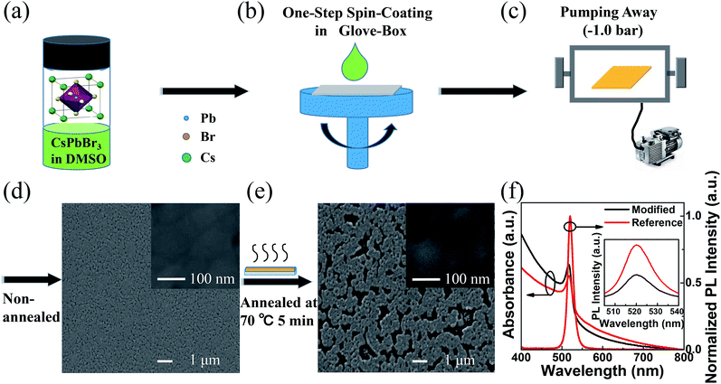 |
| | Fig. 1 The schematic diagram of (a) preparation of 10 wt% CsPbBr3 in DMSO precursor solution, (b) one-step spin-coating method, (c) pumping away method, (d) the top-view SEM image of modified neat CsPbBr3 film without annealing only pumping away, (e) the top-view SEM image of reference neat CsPbBr3 film which is annealed at 70 °C for 5 min after pumping away, (f) the absorption and normalized PL spectra of modified and reference neat CsPbBr3 film. The inset exhibits the PL intensity of modified and reference neat CsPbBr3 films excited with equal light intensity at 365 nm. | |
3.2 PeLEDs performance
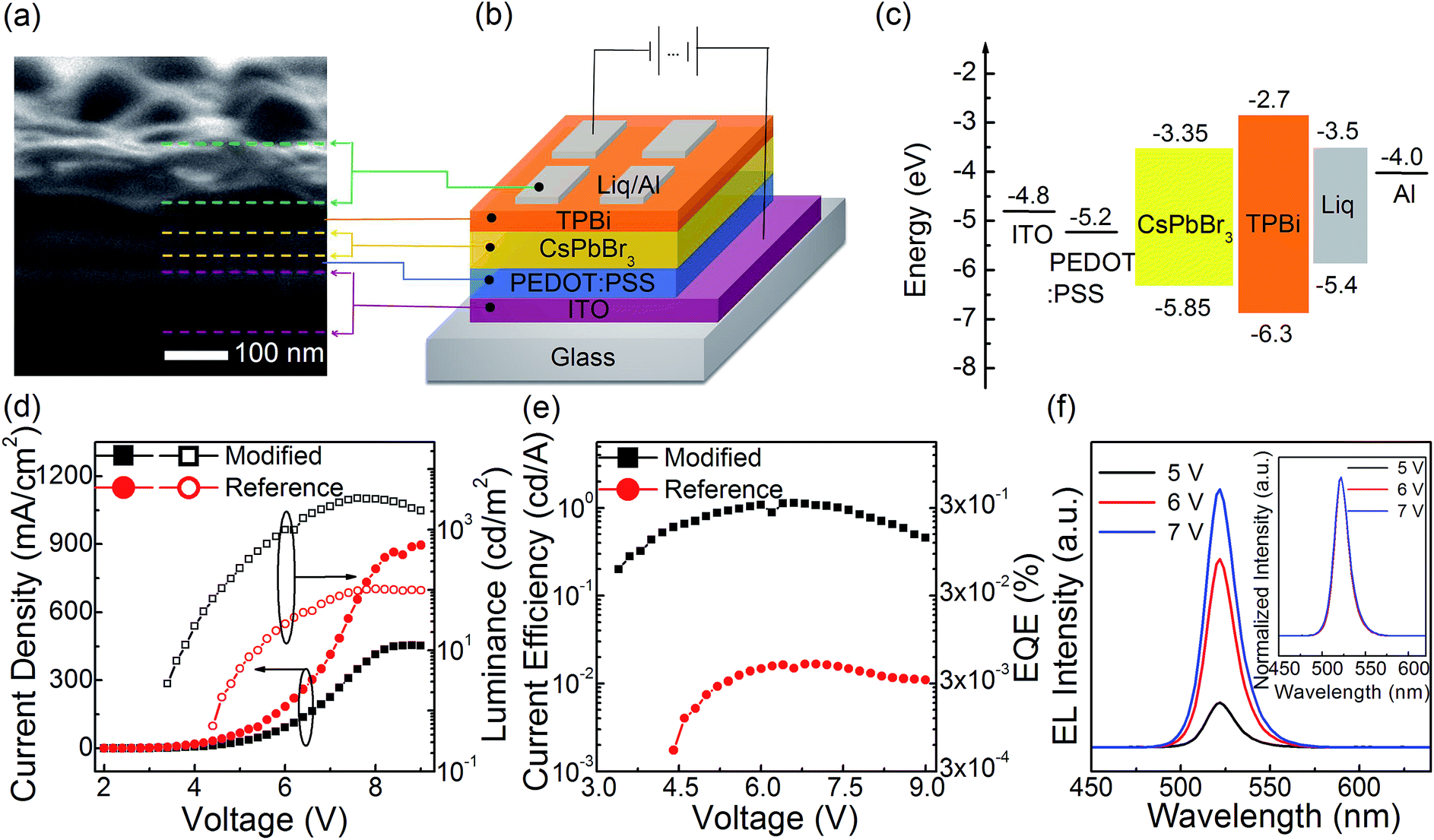
Using the modified neat CsPbBr3 film as the light emitter, the PeLEDs exhibit improved EL performance. The PeLEDs employ a typical layered structure of ITO/PEDOT:PSS30 nm/(reference or modified) neat CsPbBr3 film/TPBi65 nm/Liq2.5 nm/Al. According to the cross-section SEM image of the PeLEDs (Fig. 2a), the thickness of the modified neat CsPbBr3 film is estimated to ∼30 nm. The schematic diagram of the PeLEDs structure is shown section SEM image of the neat CsPbBr3 film based PeLEDs. The energy level diagram of each layer is shown in Fig. 2c, and all energy level values were taken from literature.26–28 The current density–voltage–luminance (J–V–L) relationship and the current efficiency–voltage–EQE (CE–V–EQE) relationship are shown in Fig. 2d and e, respectively. From J–V relationship, the modified neat CsPbBr3 film based PeLEDs exhibit lower density than reference film based ones at each applied voltage. It suggests that less current leakage in the modified PeLEDs than that in the reference ones due to higher film coverage and less pinholes in the modified film which is consistent to the top-view SEM results. From the L–V relationship and CE–V–EQE relationship, the modified neat CsPbBr3 film based PeLEDs exhibit higher luminance, current efficiency and EQE than the reference film based ones at each applied voltage, and showing maximum luminance of 3285 cd m−2, maximum current efficiency of 1.13 cd A−1 and maximum EQE of 0.29%, which are 30 times more than that of the PeLEDs with annealing process (70 °C/5 min) showing maximum luminance of 103 cd m−2, maximum current efficiency of 0.017 cd A−1 and maximum EQE of 0.004%. The enhance EL performance can be attributed to both higher film coverage which can make the current leakage decreased16,26 and smaller grain size which can spatially limit the diffusion length of excitons or charge carriers and decrease the possibility of exciton dissociation into carriers. Fig. 2f shows the EL spectra of modified neat CsPbBr3 film based PeLEDs at different applied voltage, which exhibit a high color purity of FWHM ∼18 nm and a peak wavelength located at 522 nm. In the inset of Fig. 2f, the EL color is stable and the shapes of the EL spectra are independent with applied voltage, which suggest that CsPbBr3 PeLEDs can be potentially adopted as good light sources.
 |
| | Fig. 2 (a) The cross-section SEM image of the PeLEDs with modified neat CsPbBr3 film, (b) the schematic diagram of the PeLEDs structure, (c) energy level diagram of PeLEDs, (d) J–V–L characteristics of the PeLEDs, (e) CE–V–EQE relationship of the PeLEDs, (f) EL spectra of the PeLEDs based on modified neat CsPbBr3 film applied at different voltages of 5 V, 6 V, and 7 V. The inset shows the normalized EL spectra of the modified neat CsPbBr3 film based PeLEDs working at 5 V, 6 V, and 7 V. | |
3.3 Optimizations of PeLEDs
The improved EL performance of modified film based PeLEDs can be attributed to the higher film coverage and smaller grain size, which are related to the facile and efficient film post-treatment process of only pumping away method. To further investigate the physical mechanism for the enhanced EL performance in CsPbBr3 PeLEDs with only pumping away, both the optimization of the CsPbBr3 concentration in DMSO precursor solution and the optimization of the molar ratio of PbBr2 to CsBr will be discussed.
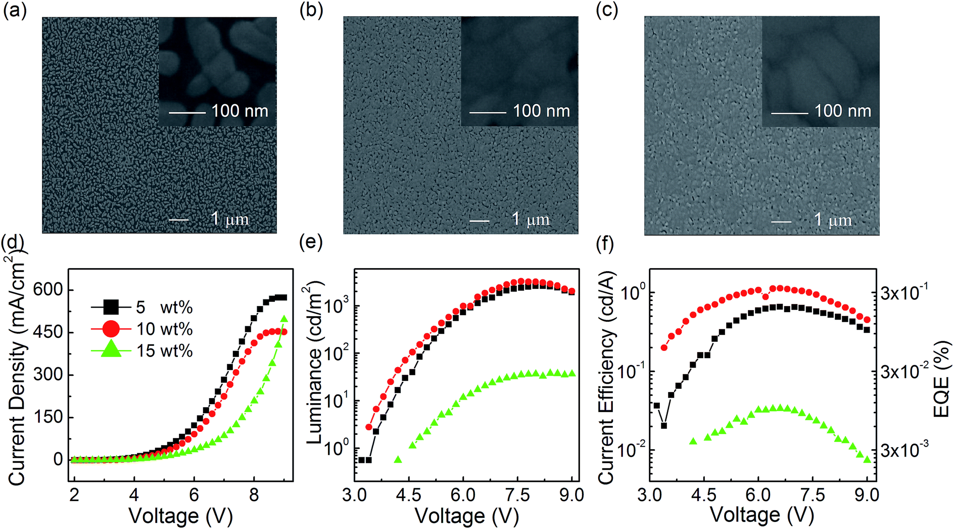
3.3.1 Optimization for the CsPbBr3 concentration. Fig. 3a, b and c show the top-view SEM images of modified neat CsPbBr3 films (with only pumping away) deposited from concentrations of 5 wt%, 10 wt%, and 15 wt% in DMSO precursor solution, respectively. For all the films with different concentrations, CsPbBr3 grains are irregular, which are just as same as the published results in ref. 19. It can be found that both the film coverage rate and the size of the grains rise with the increase of CsPbBr3 concentration in DMSO. The coverage rates and grain sizes are estimated to ∼49.1% and ∼90 nm, ∼91.1% and ∼100 nm, ∼96.9% and ∼130 nm for the films with concentrations of 5 wt%, 10 wt% and 15 wt%, respectively. From the J–V relationship (Fig. 3d), L–V relationship (Fig. 3e) and CE–V–EQE relationship (Fig. 3f), it can be found that the current density decreases with the increase of CsPbBr3 concentration at each applied voltage, while the PeLEDs based on the 10 wt% CsPbBr3 film reveals the best EL performance with maximum luminance of 3285 cd m−2, maximum current efficiency of 1.13 cd A−1, and maximum EQE of 0.29% (Fig. 3e). Two factors should be take into consideration for the best EL performance in modified 10 wt% CsPbBr3 film based PeLEDs film coverage and grain size. The coverage rates of modified CsPbBr3 film with concentrations of 10 wt% are higher than that of modified CsPbBr3 film with concentrations of 5 wt%, but lower than that of modified CsPbBr3 film with concentrations of 15 wt%. And grain sizes of modified CsPbBr3 films with concentrations of 10 wt% are larger than that of modified CsPbBr3 film with concentrations of 5 wt%, but smaller than that of modified CsPbBr3 film with concentrations of 15 wt%. The lower coverage rate makes the current leakage increase, which is bad to the EL performance of PeLEDs, while the smaller grains make the excitons undergo radiative recombination, which is beneficial to the EL performance of PeLEDs. These two aspects compete mutually and the current efficiency (CE) is defined as: CE = L/J, where the L and J represent the luminance and current density at each applied voltage of the PeLEDs, respectively. As a result, the PeLEDs using 10 wt% CsPbBr3 film exhibit the best EL performance with suitable coverage rate and grain size. Meanwhile, for the PeLEDs using 5 wt% CsPbBr3 film show a greater current density at each applied voltage and an inferior EL performance compared to PeLEDs based on 10 wt% CsPbBr3 film, which suggests that the lower coverage rate plays a leading role in weakening the EL performance in 5 wt% CsPbBr3 film based PeLEDs. When it comes to the PeLEDs using 15 wt% CsPbBr3 film, it exhibits a lower current density at each applied voltage and an inferior EL performance compared to PeLEDs based on 10 wt% CsPbBr3 film, which suggests that larger grain size plays a leading role to reduce the current efficiency in the PeLEDs with 15 wt% CsPbBr3 film.
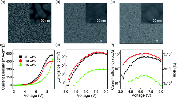 |
| | Fig. 3 The top-view SEM image of modified neat CsPbBr3 film with only pumping away from different concentrations of (a) 5 wt%, (b) 10 wt%, (c) 15 wt% in DMSO precursor solution, (d) J–V–L relationship, (e) L–V of the PeLEDs, (f) CE–V–EQE relationship of the PeLEDs based on different CsPbBr3 concentrations in DMSO precursor solution. | |
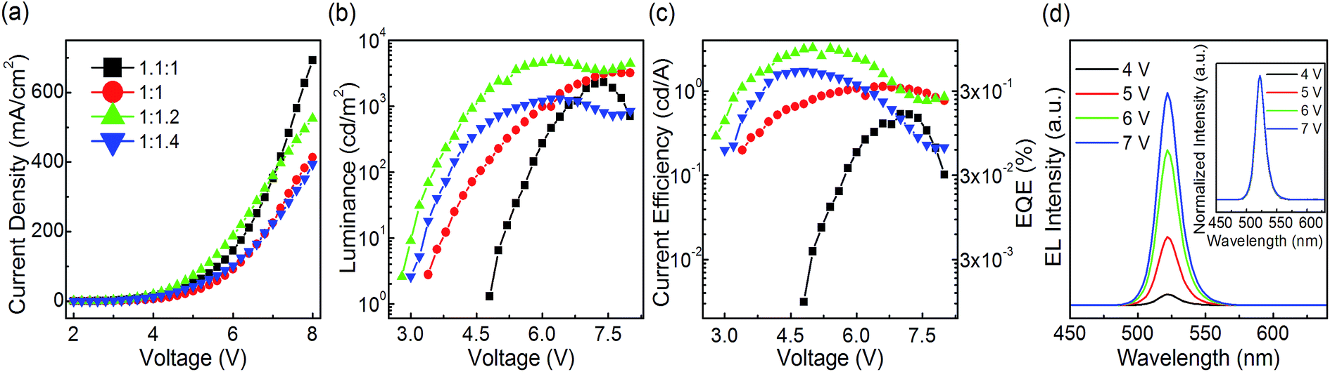
3.3.2 Optimization for the molar ratio of PbBr2 to CsBr. Besides optimization for the CsPbBr3 concentration in DMSO precursor solution, the PeLEDs with different molar ratios of PbBr2 to CsBr equaling to 1.1:1, 1:1, 1:1.2, and 1:1.4 at a 10 wt% CsPbBr3 concentration in DMSO precursor solution are fabricated with only pumping away process. From the J–V curves, the PeLEDs based on the molar ratio of PbBr2 to CsBr equaling to 1:1.2 exhibit the largest current density among all PeLEDs at each applied voltage lower than 7 V. When it comes to the L–V relationship, the PeLEDs with a molar ratio of PbBr2 to CsBr of 1:1.2 exhibit the highest maximum luminance of 5046 cd m−2 and lowest turn on voltage of 2.8 V among all the devices. Moreover, the current efficiency and EQE of the PeLEDs with a molar ratio of PbBr2 to CsBr equaling to 1:1.2 show the best with maximum current efficiency of 3.25 cd A−1 and maximum EQE of 0.85% among all the devices, which is among the best results based on neat CsPbBr3 PeLEDs reported so far. It should be noted that the maximum current efficiency and the maximum EQE of PeLEDs increase with the CsBr proportion increasing in all the PeLEDs. This enhancement in EL performance is attributed to the Br-rich passivation that can reduce the halogen vacancies (VBr) (e.g. decreasing the non-radiative recombination), and thus leading to improved EL performance. This is verified by previous theoretical29 studying. Previous theoretical density functional theory (DFT) demonstrate that the presence of VBr on CsPbBr3 plays a role as defects within the band gap and acts as recombination centers. The deposition from CsBr-rich solution may reduce the probability of VBr formation on the films and hence reduce the non-radiative defect densities. And this is demonstrated by previous experimental19 and the time-resolved PL measurements we conducted. The time-resolved PL spectra are exhibited in the Fig. S2.† The average radiative recombination lifetime of the 1:1.2 neat CsPbBr3 films (0.86 ns) with only pumping away is larger than 1:1 neat CsPbBr3 films (0.82 ns). The result suggests that Br additive can effectively passivate the grain boundaries, and thus reducing non-radiation recombination, leading to enhanced the EL performance in the 1:1.2 neat CsPbBr3 films based PeLEDs. And the PeLEDs with molar ratio of 1:1.2 also show stable color with a high color purity of FWHM ∼18 nm and a peak wavelength located at 522 nm at different applied voltages (show in Fig. 4d and its inset).
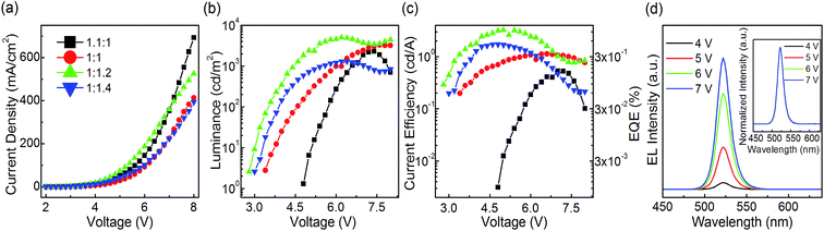 |
| | Fig. 4 (a) J–V relationship, (b) L–V relationship, (c) CE–V–EQE relationship of the PeLEDs with only pumping away and different molar ratios of PbBr2 to CsBr of 1.1:1, 1:1, 1:1.2, and 1:1.4 at a 10 wt% CsPbBr3 concentration in DMSO precursor solution, (d) EL spectra of the PeLEDs based on modified neat CsPbBr3 film molar ratio of PbBr2 to CsBr of 1:1.2 at a 10 wt% CsPbBr3 concentration in DMSO precursor solution with applied at different voltages of 4 V, 5 V, 6 V, and 7 V. The inset shows the normalized EL spectra of the modified neat 10 wt% CsPbBr3 PeLEDs based on the molar ratio of PbBr2 to CsBr equaling to 1:1.2 working at 4 V, 5 V, 6 V, and 7 V. | |
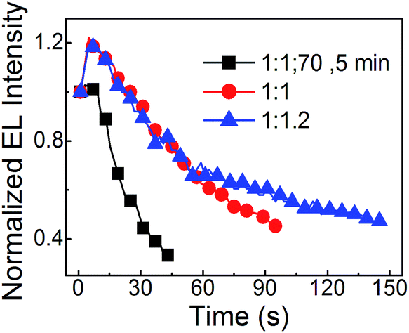
3.3.3 The stability of PeLEDs. As shown in Fig. 5, the stability of both equal molar ratio of PbBr2:CsBr and CsBr rich (PbBr2:CsBr = 1:1.2) neat CsPbBr3 PeLEDs with just pumping away are better than that of neat CsPbBr3 PeLEDs with annealing. The half lifetimes (which is the time duration from the initial luminance of 100 cd m−2 decreasing to half luminance of the initial luminance) of the three PeLEDs formed by PbBr2:CsBr = 1:1 with annealing at 70 °C for 5 min after pumping away, PbBr2:CsBr = 1:1 with just pumping away, and PbBr2:CsBr = 1:1.2 with just pumping away are estimated to 29 s, 87 s and 135 s, respectively. It indicates that the pumping away process and the Br rich method are benefit to make the PeLEDs more stable.
 |
| | Fig. 5 The stability of PeLEDs formed by PbBr2:CsBr = 1:1 with annealing at 70 °C for 5 min after pumping away, PbBr2:CsBr = 1:1 with just pumping away, and PbBr2:CsBr = 1:1.2 with just pumping away. | |
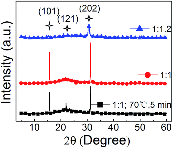
3.4 XRD patterns of perovskite films
In Fig. 6, the XRD patterns of the three neat CsPbBr3 films (PbBr2:CsBr = 1:1 with annealing at 70 °C for 5 min after pumping away, PbBr2:CsBr = 1:1 with just pumping away, PbBr2:CsBr = 1:1.2 with just pumping away) indicate that orthorhombic crystal structures are realized. And no additional peak for the solvent residue are found in the XRD patterns, which means that there is no solvent residue in all the three films. To further confirm it, the UV-Vis absorption spectra are shown in Fig. S3,† and similar absorption shapes are demonstrated. These results suggest that the structures and the optical properties of perovskite films with just pumping away are same with that of the one with annealing, which may not do bad effects to the EL performance.
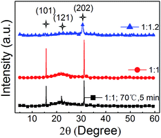 |
| | Fig. 6 The XRD patterns of three 10 wt% neat CsPbBr3 films (PbBr2:CsBr = 1:1 with annealing at 70 °C for 5 min after pumping away, PbBr2:CsBr = 1:1 with just pumping away, PbBr2:CsBr = 1:1.2 with just pumping away). | |
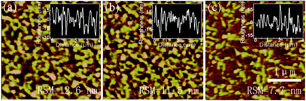
3.5 AFM images of perovskite films
AFM images are performed and are shown in Fig. 7. For the neat 1:1 CsPbBr3 films, the annealed one exhibits a larger roughness of 12.6 nm compared to the one without annealing (11.5 nm), which indicating that annealing after the pumping away process will do bad effect to the morphology of the perovskite film and leading to worse EL performance of the PeLED with annealed neat 1:1 CsPbBr3 film. And with only pumping away process, the surface roughness can be further reduced to 7.7 nm by Br rich CsPbBr3 film with PbBr2:CsBr equaling to 1:1.2. Thus, with the smoothest CsPbBr3 film, the PeLEDs with molar ratio of 1:1.2 achieved the best EL performance.
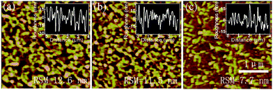 |
| | Fig. 7 AFM images for three 10 wt% neat CsPbBr3 films (a) PbBr2:CsBr = 1:1 with annealing at 70 °C for 5 min after pumping away, (b) PbBr2:CsBr = 1:1 with just pumping away, (c) PbBr2:CsBr = 1:1.2 with just pumping away. | |
4 Conclusion
The simple and effective method of only pumping away process is demonstrated to fabricate equimolar and CsBr-rich CsPbBr3 PeLEDs with enhanced EL performance of maximum luminance of 3285 cd m−2 and 5046 cd m−2, maximum current efficiency of 1.13 cd A−1 and 3.25 cd A−1 and EQE of 0.29% and 0.85%, which are 30 folds more than that of the equimolar ones with 70 °C/5 min annealing process after pumping away process. The only pumping away process benefits to obtain high quality CsPbBr3 film with higher coverage, smaller grains better Br-rich passivation, and smoother surface, which lead to less current leakage, and larger possibility of exciton radiative decay, and thus achieving better EL performance and longer stability in PeLEDs with only pumping away. The work therefore offers some helpful implications in developing high-performance PeLEDs.
Conflicts of interest
There are no conflicts of interest to declare.
Acknowledgements
We acknowledge financial support from the Natural Science Foundation of China (Grant No. 61404108, 11504300 and 11374242), and Fundamental Research Funds for the Central Universities (Grant No. XDJK2017D140). And authors thank for Prof. Guo-Qing Li, Prof. Hu-Zhi Zheng, and Prof. Yuan-Fang Li (Southwest University) for their help related to experiments and fruitful discussions.
Notes and references
- Z. K. Tan, R. S. Moghaddam, M. L. Lai, P. Docampo, R. Higler, F. Deschler, M. Price, A. Sadhanala, L. M. Pazos, D. Credgington, F. Hanusch, T. Bein, H. J. Snaith and R. H. Friend, Nat. Nanotechnol., 2014, 9, 687–692 CrossRef CAS PubMed.
- G. R. Li, F. W. R. Rivarola, N. J. L. K. Davis, S. Bai, T. C. Jellicoe, F. D. L. Pena, S. C. Hou, C. Ducati, F. Gao, R. H. Friend, N. C. Greenham and Z. K. Tan, Adv. Mater., 2016, 28, 3528–3534 CrossRef CAS PubMed.
- M. Kulbak, D. Cahen and G. Hodes, J. Phys. Chem. Lett., 2015, 6, 2452–2456 CrossRef CAS PubMed.
- F. Palazon, F. D. Stasio, Q. A. Akkerman, R. Krahne, M. Prato and L. Manna, Chem. Mater., 2016, 28, 2902–2906 CrossRef CAS PubMed.
- C. C. Stoumpos, C. D. Malliakas, J. A. Peters, Z. F. Liu, M. Sebastian, J. Im, T. C. Chasapis, A. C. Wibowo, D. Y. Chung, A. J. Freeman, B. W. Wessels and M. G. Kanatzidis, Cryst. Growth Des., 2013, 13, 2722–2727 CAS.
- S. Colella, M. Mazzeo, A. Rizzo, G. Gigli and A. Listorti, J. Phys. Chem. Lett., 2016, 7, 4322–4334 CrossRef CAS PubMed.
- X. M. Li, Y. Wu, S. L. Zhang, B. Cai, Y. Gu, J. Z. Song and H. B. Zeng, Adv. Funct. Mater., 2016, 26, 2435–2445 CrossRef CAS.
- G. P. Li, H. Wang, T. Zhang, L. F. Mi, Y. G. Zhang, Z. P. Zhang, W. J. Zhang and Y. Jiang, Adv. Funct. Mater., 2016, 26, 8478–8486 CrossRef CAS.
- Y. H. Kim, H. Cho and T. W. Lee, Proc. Natl. Acad. Sci. U. S. A., 2016, 113, 11694–11702 CrossRef CAS PubMed.
- H. Cho, S. H. Jeong, M. H. Park, Y. H. Kim, C. Wolf, C. L. Lee, J. H. Heo, A. Sadhanala, N. S. Myoung, S. Yoo, S. H. Im, R. H. Friend and T. W. Lee, Science, 2015, 350, 1222–1225 CrossRef CAS PubMed.
- J. Z. Song, J. H. Li, X. M. Li, L. M. Xu, Y. H. Dong and H. B. Zeng, Adv. Mater., 2015, 27, 7162–7167 CrossRef CAS PubMed.
- Y. H. Song, J. S. Yoo, B. K. Kang, S. H. Choi, E. K. Ji, H. S. Jung and D. H. Yoon, Nanoscale, 2016, 8, 19523–19526 RSC.
- X. L. Zhang, B. Xu, J. B. Zhang, Y. Gao, Y. J. Zheng, K. Wang and X. W. Sun, Adv. Funct. Mater., 2016, 26, 4595–4600 CrossRef CAS.
- H. Huang, H. Lin, S. V. Kershaw, A. S. Susha, W. C. H. Choy and A. L. Rogach, J. Phys. Chem. Lett., 2016, 7, 4398–4404 CrossRef CAS PubMed.
- X. Y. Zhang, H. Lin, H. Huang, C. Reckmeier, Y. Zhang, W. C. H. Choy and A. L. Rogach, Nano Lett., 2016, 16, 1415–1420 CrossRef CAS PubMed.
- J. Q. Li, X. Shan, S. G. R. Bade, T. Geske, Q. L. Jiang, X. Yang and Z. B. Yu, J. Phys. Chem. Lett., 2016, 7, 4059–4066 CrossRef CAS PubMed.
- X. Y. Zhang, C. Sun, Y. Zhang, H. Wu, C. Y. Ji, Y. H. Chuai, P. Wang, S. P. Wen, C. F. Zhang and W. W. Yu, J. Phys. Chem. Lett., 2016, 7, 4602–4610 CrossRef CAS PubMed.
- J. H. Li, L. M. Xu, T. Wang, J. Z. Song, J. W. Chen, J. Xue, Y. H. Dong, B. Cai, Q. S. Shan, B. N. Han and H. B. Zeng, Adv. Mater., 2017, 29, 1603885 CrossRef PubMed.
- N. Yantara, S. Bhaumik, F. Yan, D. Sabba, H. A. Dewi, N. Mathews, P. P. Boix, H. V. Demir and S. Mhaisalkar, J. Phys. Chem. Lett., 2015, 6, 4360–4364 CrossRef CAS PubMed.
- Y. C. Ling, Y. Tian, X. Wang, J. C. Wang, J. M. Knox, F. Perez-Orive, Y. J. Du, L. Tan, K. Hanson, B. W. Ma and H. W. Gao, Adv. Mater., 2016, 28, 8983–8989 CrossRef CAS PubMed.
- L. Song, X. Y. Guo, Y. S. Hu, Y. Lv, J. Lin, Z. Q. Liu, Y. Fan and X. Y. Liu, J. Phys. Chem. Lett., 2017, 8, 4148–4154 CrossRef CAS PubMed.
- Z. H. Wei, A. Perumal, R. Su, S. Sushant, J. Xing, Q. Zhang, S. T. Tan, H. V. Demir and Q. H. Xiong, Nanoscale, 2016, 8, 18021–18026 RSC.
- G. R. Li, M. Price and F. Deschler, APL Mater., 2016, 4, 091507 CrossRef.
- L. Protesescu, S. Yakunin, M. I. Bodnarchuk, F. Krieg, R. Caputo, C. H. Hendon, R. X. Yang, A. Walsh and M. V. Kovalenko, Nano Lett., 2015, 15, 3692–3696 CrossRef CAS PubMed.
- H. C. Yoon, H. Kang, S. Lee, J. H. Oh, H. Yang and Y. R. Do, ACS Appl. Mater. Interfaces, 2016, 8, 18189–18200 CAS.
- P. Chen, Z. Y. Xiong, X. Y. Wu, M. Shao, X. J. Ma, Z. H. Xiong and C. H. Gao, J. Phys. Chem. Lett., 2017, 8, 1810–1818 CrossRef CAS PubMed.
- S. I. Yoo, J. A. Yoon, N. H. Kim, J. W. Kim, J. S. Kang, C. B. Moon and W. Y. Kim, J. Lumin., 2015, 160, 346–350 CrossRef CAS.
- V. K. Ravi, G. B. Markad and A. Nag, ACS Energy Lett., 2016, 1, 665–671 CrossRef CAS.
- H. L. Shi and M. H. Du, Phys. Rev. B: Condens. Matter Mater. Phys., 2014, 90, 174103 CrossRef.
Footnote |
| † Electronic supplementary information (ESI) available. See DOI: 10.1039/c7ra09484a |
|
| This journal is © The Royal Society of Chemistry 2017 |
Click here to see how this site uses Cookies. View our privacy policy here. 
 Open Access Article
 This Open Access Article is licensed under a
  *
*