
 Open Access Article
 This Open Access Article is licensed under a
 Creative Commons Attribution 3.0 Unported Licence
Layer-number dependent and structural defect related optical properties of InSe†
T. Zhenga,
Z. T. Wua,
H. Y. Nana,
Y. F. Yua,
A. Zafara,
Z. Z. Yana,
J. P. Lu *a and
Z. H. Ni*ab
*a and
Z. H. Ni*ab
aSchool of Physics, Southeast University, Nanjing 211189, China. E-mail: phyljp@seu.edu.cn; zhni@seu.edu.cn
bState Key Laboratory for Modification of Chemical Fibers and Polymer Materials, Donghua University, Shanghai 201620, China
First published on 1st December 2017
Abstract
Two-dimensional (2D) InSe is an attractive semiconductor because of its bandgap in the near infrared region, high carrier mobility and chemical stability. Here, we present systematic investigations on the layer-dependent optical properties of few-layer InSe (2–6 layers). We develop a quantitative calibration map using optical images and Raman and photoluminescence (PL) spectroscopy to directly identify the layer numbers of the InSe flakes. This is facilitated by the significant difference in the optical contrast or Raman/PL spectra of InSe with different thicknesses. Moreover, excitonic states in few-layer InSe and in the bulk are probed by temperature-dependent PL spectroscopy. An emerging peak arising from the recombination of excitons bound to localized states is observed at low temperature. These states arise from structural defects which can also be induced via electron beam irradiation. The PL emission from bound excitons could be modified to be even stronger than the emission from near band edge recombination. This provides a new strategy to improve the PL emission efficiency of 2D InSe.
Introduction
Two-dimensional (2D) layered materials, including semi-metallic graphene,1–3 semiconducting transition metal dichalcogenides (TMDs)4–7 and insulating hexagonal boron nitride (hBN), have attracted increasing attention in the past decade. The features of near-ballistic transport behavior at room temperature and high mobility8,9 make graphene promising in the application of next generation electronics,10–12 but its gapless characteristic restricts its applications in logic and optoelectronic devices.13 To overcome this weakness, TMDs have been reintroduced and widely investigated because of their intrinsic bandgap, but their mobility is relatively low.14 In addition to TMDs, transitional metal monochalcogenides (TMMs) are typical semiconductors with bandgaps covering the range from UV to near-infrared (NIR). Recent reports have demonstrated that layered TMMs have promising potential in electronics and optoelectronics, for example, the valleytronic properties of SnS,15 high mobility of GeS,16 superior photodetection of GaSe,17 and so forth.18–23Among these TMMs, InSe is an emerging material with the layer-dependent bandgap ranging from 1.25 eV (bulk) to 1.9 eV (bilayer) and it exhibits direct-to-indirect bandgap transition with decreasing thickness.24,25 Few-layers InSe possesses high electron mobility, exceeding 103 cm2 V−1 s−1 at room temperature.24 Recently, researches have been carried out to explore the optical properties of InSe few layers. For example, the thickness-dependent optical contrast,26,27 photoluminescence (PL) and Raman spectra24,28 have been observed. However, a systematic calibration map in using these thickness-dependent properties to identify the layer numbers of InSe is absent. In addition, the efficiency of PL emission of InSe thin layers is extremely low due to the direct-to-indirect band gap transition28 and environmental impacts.24 This restricts its potentials in optoelectronic applications. To improve the PL efficiency of 2D InSe, deep understanding of the excitonic fundamentals like the recombination mechanism, thermal perturbation, and dielectric surroundings is desired.
Herein, we carry out systematic investigations on the optical properties of InSe few layers. Significant layer dependences are observed on the optical contrast, Raman and PL spectra collecting from InSe flakes with different thicknesses. A calibration map is thereby developed to quantitatively identify the layer numbers based on these properties. Evolution of the excitonic states is further investigated by means of the temperature-dependent PL spectra. In addition, the optical properties of the InSe flakes could be efficiently modified via electron beam irradiation, which could introduce localized states. The PL emission from the recombination of excitons bounded to these states could be even stronger than the emission from band edge recombination after modification.
Experimental
Thin InSe flakes were mechanically exfoliated from n-doped InSe (Fig. ESI1†) crystals and transferred onto a Si substrate with 300 nm SiO2 coating layer. A microscope was used to obtain optical images of the samples and Matlab software was utilized to read out the red (R), green (G), blue (B) values at each pixel of the optical images and get the histogram of optical contrast distribution.29 Atomic force microscope (AFM) was employed to confirm the thickness of InSe flakes. Raman and PL spectra were collected using a LabRAM HR800 Raman system (excitation wavelength = 532 nm). Temperature-dependent spectra were collected in a Montana Instruments cryostation low-temperature system.Result and discussion
Charge-coupled device (CCD) in optical microscope allows us to capture digital images of samples, from which we could get R, G and B values based on the color filters in CCD and reproduce a reflection spectrum from the surface of the sample.30 Fig. 1 illustrates the process of thickness identification via optical contrast. Fig. 1(a) shows the optical image of an InSe flake deposited on a SiO2/Si substrate (optical images of 4-layer and 5-layer film are given in Fig. ESI2†). Evidently, the contrast values of the domains with different thicknesses are easily resolved in the G channel image (Fig. 1(b)). According to the extracted histogram of the optical contrast distribution, representing contrast of substrate and two domains (region B and A) with different thicknesses are measured to be ∼0 (substrate), ∼−0.088 and ∼−0.179, respectively (Fig. 1(c)). AFM results indicate that the thickness of region B and region A is ∼2.1 and ∼3.2 nm, respectively (Fig. 1(e and f)). Considering the thickness of a monolayer InSe (∼0.83 nm)27 and also the instrument offset of AFM (∼0.5 nm), region A and B are corresponding to three layers and two layers. After mutual authentication between optical contrast and AFM results, the contrast values present one-to-one correspondence to the layer numbers of InSe few-layers (Fig. 1(d)). Therefore, it can be employed to easily identify the layer numbers of the exfoliated samples. The average contrast values (G channel) of 1–5 layer InSe is −0.048, −0.089, −0.161, −0.218 and −0.262, respectively.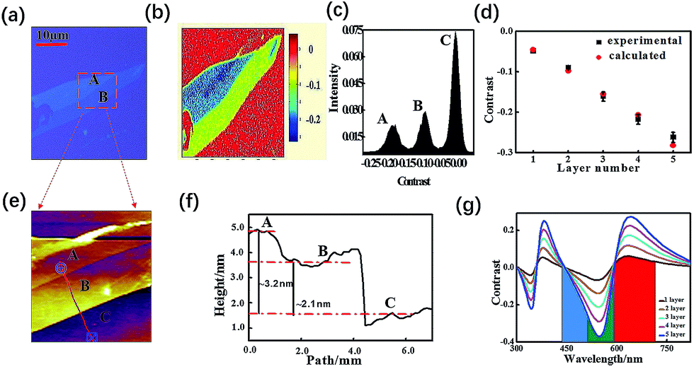 | ||
| Fig. 1 (a) Optical image of the InSe flake exfoliated onto a SiO2 (300 nm)/Si substrate. (b) G channel optical contrast image of the same flake shown in (a). (c) Histogram of optical contrast distribution, the optical contrast of substrate, A and B are 0, −0.179, −0.088, respectively. (d) Optical contrast values of InSe flakes with different thickness. (e) AFM image of red square labelled in (a). (f) AFM profile measured along the red path in (d). (g) The calculated contrast spectra of InSe with different thickness (1–5 layers) on SiO2 (300 nm)/Si substrate. | ||
Besides experimental measurements, the optical contrast could be theoretically estimated via Fresnel equation under normal incident conditions, C(λ) = [R0(λ) − R(λ)]/R0(λ)30 R0(λ) = |r0(λ)|2 and R(λ) = |r(λ)|2 are the reflected light intensities from air/SiO2/Si and air/InSe/SiO2/Si, respectively, which are wavelength dependent,
| r0(λ) = (r02 + r23e−2iϕ2)/(1 + r02r23e−2iϕ2) | (1) |
| r(λ) = [r01 + r01r12r23e−2iϕ2 + r12e−2iϕ1 + r23e−2i(ϕ1+ϕ2)] × [1 + r12r23e−2iϕ2 + r01r12e−2iϕ1 + r01r23e−2i(ϕ1+ϕ2]−1 | (2) |
Under normal incidence, rij = (ni − nj)/(ni + nj) (i, j is taken from 0 to 3). n0, n1, n2 and n3 are the refractive indices of air, InSe,27 SiO2 and Si, respectively. ϕ12 = (2πn1,2d1,2)/λ is the induced phase difference when light passes through InSe or SiO2. d1 = N × d is the thickness of InSe, where N is the number of layers and d = 0.83 nm is the thickness of InSe monolayer.27 d2 represents the thickness of the SiO2 layer. Accordingly, the optical contrast (G channel) of InSe with 1–5 layers can be calculated to be −0.046, −0.098, −0.155, −0.207 and −0.282, respectively (Fig. 1(d and g)). These values are well consistent with the experimental results (Fig. 1(d)).
As has been demonstrated in InSe, the out of plane Raman modes present significant thickness-dependence.31 The Raman spectra of InSe flakes with different thickness are collected at room temperature (Fig. 2(a)). Evidently, bulk-InSe exhibits modes whose frequency of characteristic vibrations are ∼114 cm−1 (A1), ∼175 cm−1 (E), ∼198 cm−1 (A1(LO)) and ∼225 cm−1 (A1).31 As thickness decreases, the frequency of the out-of-plane non-polar A1 mode at ∼114 cm−1 decreases and the polar A1 (LO) mode significantly increases (Fig. 2(a and b)), whilst, the shifts of A1 mode at ∼225 cm−1 is inconspicuous. The blue-shift of A1 (LO) mode with decreasing thickness arises from the stronger In–Se bond in thinner layers. It has been demonstrated that the In–Se bond is much stronger in monolayer than in bulk.31 The stronger bond gives rise to higher frequency of vibrations. However, in low frequency, the restoring forces of A1 at ∼114 cm−1 are mainly from interlayer interactions of In–In bond. The gradually weakened interlayer interaction of In–In bond leads to decreasing frequency of A1 mode. Consequently, the layer dependences of low frequency A1 mode and A1 (LO) mode could be utilized to identify the layer number of InSe, as summarize in Fig. 2(b). Theoretical calculations have predicted that the electronic band structure of InSe is strongly dependent on the thickness.24,32 Correspondingly, the PL behavior is expected to present evident variation with the thickness. PL spectra are taken from InSe flakes and shown in Fig. 2(c) (normalized by the power of incident laser, wavelength of laser is 532 nm and the power is ∼100 μW, size of laser spot after focusing is about 2 μm, temperature = 4 K). Evidently, the PL intensity strongly decreases with reducing thickness. This is most probably attributed to the direct-to-indirect bandgap transition caused by quantum confinement analogous to the case of InSe nanoparticles.33,34 One of the central questions about the PL is regarding the nature of the lowest energy transition in terms of the initial and final momentum states. In the case of bulk InSe, the top of the valence band and the bottom of the conduction band are both at Γ and the lowest energy transition is therefore momentum allowed; this is a direct transition. When InSe is thinned down, a slightly higher local minimum of the conduction band is at the M point and the corresponding Γ → M transition is a much less intense, leading to momentum-forbidden indirect transition. It has been demonstrated that the direct-to-indirect bandgap transition occurs at a critical thickness of 5 nm.28 This is consistent with our observation that the decrease of the PL signal starting at the flakes with thickness of 6 layers. In addition to the direct-to-indirect bandgap transition, broadening of the bandgap is a more significant effect of the quantum confinement. Because of the relatively smaller bandgap and reduced exciton mass (μ//c = 0.054 along the z-axis), quantum confinement in InSe thin layers is strong.28 As a result, the peak position of PL gradually shifts from ∼1.3 eV to ∼1.9 eV with decreasing thickness from bulk to bilayer, as summarized in Fig. 2(d). Considering that PL intensity is sensitive to the ambient conditions, it would be easily affected by the external environment. Therefore, the layer-dependence of peak position is a more effective approach to identify the layer number of InSe.
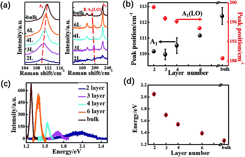 | ||
| Fig. 2 (a) Raman spectra of InSe with different thicknesses. (b) The positions of different peaks with the change of layer numbers. (c) PL spectra of InSe with different layers, and the peak positions are shown in (d). | ||
To get a deeper understanding on the origins of the particular excitonic states, temperature dependent PL spectra are taken from representative samples of InSe (Fig. 3(a–d)). The peak position of ∼1.73 eV (at 8 K, Fig. 3(a)) is consistent with the measured bandgap of InSe trilayer.24 Therefore, the PL emission of trilayer is attributed to the recombination of excitons at near band edge. The peak intensity decreases with increasing temperature, while the peak position red-shifts (Fig. 3(e and f)). The significant decrease of the peak intensity is most probably due to the thermal perturbation. At higher temperature, the promoted phonon oscillation would accelerate non-radiative recombination and lead to the decline of PL emission. Meanwhile, the exciton–phonon interactions would be significantly enhanced with increasing temperature. This could also contribute to the red-shift of the peak position together with the influence of thermal expansion.35,36 At lower temperature, the oscillations of phonons are suppressed.
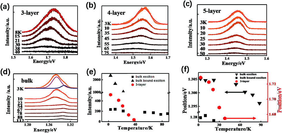 | ||
| Fig. 3 (a) PL spectra of 3-layer (a), 4-layer (b), 5-layer (c) and bulk (d) InSe collected at different temperature, and the laser power is 0.1 mW, 0.03 mW, 0.03 mW and 2.3 mW, respectively. Temperature dependence of PL intensity (e) and peak position (f) of 3-layer and bulk InSe. | ||
The exciton–phonon scattering is dominated by phonon absorption. With increasing temperature, the contribution to the exciton scattering from phonon emission becomes comparable to the phonon absorption. This facilitates the red-shift of the PL emission.37 Similar phenomena are also observed in the InSe four-layer and five-layer samples (Fig. 3(b and c)). Remarkably, the PL spectra of the InSe bulk consist of two peaks. After Lorentz curve fitting, the peaks are identified at ∼1.28 and ∼1.31 eV, respectively. The later one could be attributed to the recombination of the exciton at near band edge, according to the value of bandgap of InSe bulk.24 The intensities of these two peaks decrease and the peaks red-shift with increasing temperature (Fig. 3(e and f)). However, the peak with lower energy decreases more significantly and disappears at ∼54 K. This is in accordance with characteristics of bound exciton emission resulting from structural defects.38,39 To further verify the origination of this emerging PL emission, we expose the sample to electron beam irradiation to intentionally introduce structural defects into the sample. The PL spectra (4 K) are collected from the InSe bulk and 4-layer before and after modifications (Fig. 4(a and d)). Electron beam dosage of 18.4 × 106 μm−2 and 37.6 × 106 μm−2 are applied to four-layer and bulk, respectively. Evidently, the intensity of the peak at ∼1.28 eV of the bulk sample increases after electron beam modification. Similarly, a new peak (at ∼1.45 eV) emerges in the PL spectra of four-layer sample after modification in addition to the near band edge at ∼1.53 eV, while its intensity is around double of the pristine sample. To identify the origin of this enhancement, we carry out investigations on the excitation power-dependence of the PL spectra (Fig. 4(b) and (e)). The PL intensities are extracted from the spectra and plotted as a function of excitation powers, as shown in Fig. 4(c) (bulk) and Fig. 4(f) (four-layer). The experimental data could be described well by the power law: I ∝ Pα (solid lines in Fig. 4(c and f)), where I is the PL peak intensity, P is the excitation power, and α is the extracted exponent factor. The values of α are fitted to be ∼1.0 (peak at ∼1.31 eV) and ∼0.68 (peak at ∼1.28 eV) for the bulk sample, while the α values are ∼1.0 (peak at ∼1.53 eV) and ∼0.13 (peak at ∼1.45 eV) for the four-layer sample. The value of α has been demonstrated to be the indicator of the dominant origins of the PL emissions.38,40,41 α = 1 indicates that PL emissions arise from the recombination of neutral or charged excitons. α < 1 presents that the PL emissions generally originate from the recombination of excitons bounded to defects, while α > 1 demonstrates emissions from biexcitons.42 Considering the finite density of states caused by the defects, PL intensity from the bound excitons is expected to reach saturation at high excitation power. This would facilitate the case of α < 1, whereas, the free exciton intensity scales linearly without any sign of saturation. Therefore, the enhancement of the PL originates from the increasing states of active defects by means of electron beam irradiation. By carefully controlling the types and concentration of defects in InSe, e.g. by Ar, O, or H plasma irradiation, the PL emission efficiency of InSe thin flakes could be dramatically improved.43
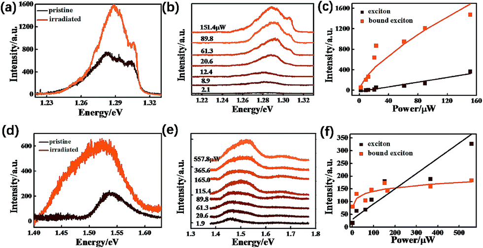 | ||
| Fig. 4 PL spectra of pristine and electron beam irradiated bulk (a) and 4-layer InSe sample (d). For bulk InSe, two peaks appear at ∼1.28 eV and ∼1.31 eV, which represent exciton and bound exciton, while in 4-layer sample, the peaks are at ∼1.45 eV and ∼1.53 eV, respectively. Power-dependent PL spectra of electron beam irradiated bulk (b) and 4-layer InSe (e), collected at 4 K. The laser power dependent PL intensities of exciton and bound exciton of bulk (c) and 4-layer InSe (f) is fitted using power law: I ∝ Pα. | ||
Conclusions
In summary, we have developed the optical approaches to facilely identify the layer numbers of InSe flakes. The identification is empowered by the significant layer-dependence of the optical contrast, Raman or PL spectra of InSe. The excitonic states in InSe few-layers and bulk have been investigated by the temperature-dependent PL spectra. Introducing structural defects into InSe via electron beam irradiation has been demonstrated as a potential approach to improve the PL emission efficiency of InSe.Conflicts of interest
There are no conflicts to declare.Acknowledgements
This work is supported by National Natural Science Foundation of China (No. 61422503 and 61376104), and the Fundamental Research Funds for the Central Universities.Notes and references
- A. C. Ferrari and D. M. Basko, Nat. Nanotechnol., 2013, 8, 235–246 CrossRef CAS PubMed.
- C. H. Lui, K. F. Mak, J. Shan and T. F. Heinz, Phys. Rev. Lett., 2010, 105, 127404 CrossRef PubMed.
- A. K. Geim and K. S. Novoselov, Nat. Mater., 2007, 6, 183–191 CrossRef CAS PubMed.
- T. Cao, G. Wang, W. Han, H. Ye, C. Zhu, J. Shi, Q. Niu, P. Tan, E. Wang, B. Liu and J. Feng, Nat. Commun., 2012, 3, 887 CrossRef PubMed.
- H. R. Gutiérrez, N. Perea-López, A. L. Elías, A. Berkdemir, B. Wang, R. T. Lv, F. López-Urías, V. H. Crespi, H. Terrones and M. Terrones, Nano Lett., 2013, 13, 3447–3454 CrossRef PubMed.
- A. Splendiani, L. Sun, Y. Zhang, T. Li and J. Kim, Nano Lett., 2010, 10, 1271–1275 CrossRef CAS PubMed.
- B. Radisavljevic, A. Radenovic, J. Brivio, V. Giacometti and A. Kis, Nat. Nanotechnol., 2011, 6, 147–150 CrossRef CAS PubMed.
- Y. B. Zhang, Y. W. Tan and H. L. Stormer, Nature, 2005, 438, 201–204 CrossRef CAS PubMed.
- X. Du, I. Skachko, A. Barker and E. Y. Andrei, Nat. Nanotechnol., 2008, 3, 491–495 CrossRef CAS PubMed.
- Z. Jiang, E. A. Henriksen, L. C. Tung, Y. J. Wang, M. E. Schwartz, M. Y. Han, P. Kim and H. L. Stormer, Phys. Rev. Lett., 2007, 98, 197403 CrossRef CAS PubMed.
- Z. Chen, Y. M. Lin, M. J. Rooks and P. Avouris, Phys. E, 2007, 40, 228–232 CrossRef CAS.
- Y. M. Lin, K. A. Jenkins, A. Valdes-Garcia, J. P. Small, D. B. Farmer and P. Avouris, Nano Lett., 2008, 9, 422–426 CrossRef PubMed.
- S. Gilbertson, G. L. Dakovski, T. Durakiewicz, J. X. Zhu, K. M. Dani, A. D. Mohite, A. Dattelbaum and G. Rodriguez, J. Phys. Chem. C, 2011, 3, 64–68 Search PubMed.
- S. Larentis, B. Fallahazad and E. Tutuc, Appl. Phys. Lett., 2012, 101, 223104 CrossRef.
- A. S. Rodin, L. C. Gomes, A. Carvalho and A. C. Neto, Phys. Rev. B, 2016, 93, 045431 CrossRef.
- F. Li, X. Liu, Y. Wang and Y. Li, J. Mater. Chem. C, 2016, 4, 2155–2159 RSC.
- P. Hu, Z. Wen, L. Wang, P. Tan and K. Xiao, ACS Nano, 2012, 6, 5988–5994 CrossRef CAS PubMed.
- X. Meng, K. He, D. Su, X. Zhang, C. Sun, Y. Ren, H. H. Wang, W. Weng, L. Trahey, C. P. Canlas and J. W. Elam, Adv. Funct. Mater., 2014, 24, 5435–5442 CrossRef CAS.
- P. A. Hu, L. Wang, M. Yoon, J. Zhang, W. Feng, X. Wang, Z. Wen, J. C. Idrobo, Y. Miyamoto, D. B. Geohegan and K. Xiao, Nano Lett., 2013, 13, 1649–1654 CrossRef CAS PubMed.
- S. Yang, Y. Li, X. Wang, N. Huo, J. B. Xia, S. S. Li and J. Li, Nanoscale, 2014, 6, 2582–2587 RSC.
- A. H. M. Kipperman and G. A. Van der Leeden, Solid State Commun., 1968, 6, 657–662 CrossRef CAS.
- X. Li, M. W. Lin, A. A. Puretzky, J. C. Idrobo, C. Ma, M. Chi, M. Yoon, C. M. Rouleau, I. I. Kravchenko, D. B. Geohegan and K. Xiao, Sci. Rep., 2014, 4, 5497 CrossRef CAS PubMed.
- S. Larentis, B. Fallahazad and E. Tutuc, Appl. Phys. Lett., 2012, 101, 223104 CrossRef.
- D. A. Bandurin, A. V. Tyurnina, G. L. Yu, A. Mishchenko, V. Zolyomi, S. V. Morozov, R. Krishna Kumar, R. V. Gorbachev, Z. R. Kudrynskyi, S. Pezzini, Z. D. Kovalyuk, U. Zeitler, K. S. Novoselov, A. Patane, L. Eaves, I. V. Grigorieva, V. I. Fal'ko, A. K. Geim and Y. Cao, Nat. Nanotechnol., 2016, 12, 223–227 CrossRef PubMed.
- M. Brotons-Gisbert, D. Andres-Penares, J. Suh, F. Hidalgo, R. Abargues, P. J. Rodríguez-Cantó, A. Segura, A. Cros, G. Tobias, E. Canadell, P. Ordejón, J. Wu, J. P. Martínez-Pastor and J. F. Sánchez-Royo, Nano Lett., 2016, 16, 3221–3229 CrossRef CAS PubMed.
- M. Brotons-Gisbert, J. F. Sánchez-Royo and J. P. Martínez-Pastor, Appl. Surf. Sci., 2015, 354, 453–458 CrossRef CAS.
- M. Brotons-Gisbert, D. Andres-Penares, J. P. Martínez-Pastor, A. Cros and J. F. Sánchez-Royo, Nanotechnology, 2017, 28, 115706 CrossRef CAS PubMed.
- G. W. Mudd, S. A. Svatek, T. Ren, A. Patanè, O. Makarovsky, L. Eaves, P. H. Beton, Z. D. Kovalyuk, G. V. Lashkarev, Z. R. Kudrynshyi and A. I. Dmitriev, Adv. Mater., 2013, 25, 5714–5718 CrossRef CAS PubMed.
- Y. Yu, Z. Li, W. Wang, X. Guo, J. Jiang, H. Nan and Z. Ni, J. Semicond., 2017, 38, 033003 CrossRef.
- Z. H. Ni, H. M. Wang, J. Kasim, H. M. Fan, T. Yu, Y. H. Wu, Y. P. Feng and Z. X. Shen, Nano Lett., 2007, 7, 2758–2763 CrossRef CAS PubMed.
- J. F. Sánchez-Royo, G. Muñoz-Matutano, M. Brotons-Gisbert, J. P. Martínez-Pastor, A. Segura, A. Cantarero, R. Mata, J. Canet-Ferrer, G. Tobias, E. Canadell, J. Marqués-Hueso and B. D. Gerardot, Nano Res., 2014, 7, 1556–1568 CrossRef.
- F. J. Manjón, A. Segura, V. Muñoz-Sanjosé, G. Tobías, P. Ordejón and E. Canadell, Phys. Rev. B: Condens. Matter Mater. Phys., 2004, 70, 125201 CrossRef.
- S. Yang and D. F. Kelley, J. Phys. Chem. B, 2005, 109, 12701–12709 CrossRef CAS PubMed.
- S. Yang and D. F. Kelley, J. Phys. Chem. B, 2006, 110, 13430–13435 CrossRef CAS PubMed.
- R. Chen, B. Ling, X. W. Sun and H. D. Sun, Adv. Mater., 2011, 23, 2199–2204 CrossRef CAS PubMed.
- J. Zhang, X. Zhang and J. Y. Zhang, J. Phys. Chem. C, 2009, 113, 9512–9515 CAS.
- J. Huang, T. B. Hoang and M. H. Mikkelsen, Sci. Rep., 2016, 6, 22414 CrossRef CAS PubMed.
- Z. Wu, Z. Luo, Y. Shen, W. Zhao, W. Wang, H. Nan, X. Guo, L. Sun, X. Wang, Y. You and Z. Ni, Nano Res., 2016, 9, 3622–3631 CrossRef CAS.
- Z. Wu, W. Zhao, J. Jiang, T. Zheng, Y. Meng, J. Lu and Z. Ni, J. Phys. Chem. C, 2017, 121, 12294–12299 CAS.
- S. Tongay, J. Suh, C. Ataca, W. Fan, A. Luce, J. S. Kang, J. Liu, C. Ko, R. Raghunathanan, J. Zhou, F. Ogletree, J. Li, J. C. Grossman and J. Wu, Sci. Rep., 2013, 3, 2657 CrossRef PubMed.
- A. A. Mitioglu, P. Plochocka, J. N. Jadczak, W. Escoffier, G. L. J. A. Rikken, L. Kulyuk and D. K. Maude, Phys. Rev. B: Condens. Matter Mater. Phys., 2013, 88, 24543 CrossRef.
- Y. You, X. Zhang, T. C. Berkelbach, M. S. Hybertsen, D. R. Reichman and T. F. Heinz, Nat. Phys., 2015, 11, 477–481 CrossRef CAS.
- H. Nan, Z. Wang, W. Wang, Z. Liang, Y. Lu, Q. Chen, D. He, P. Tan, F. Miao, X. Wang, J. Wang and Z. Ni, ACS Nano, 2014, 8, 5738–5745 CrossRef CAS PubMed.
Footnote |
| † Electronic supplementary information (ESI) available: Optical images of different-layer InSe film and transfer characteristics of InSe FET device. See DOI: 10.1039/c7ra09370e |
| This journal is © The Royal Society of Chemistry 2017 |