
 Open Access Article
 This Open Access Article is licensed under a
 Creative Commons Attribution 3.0 Unported Licence
Synthesis and thermoelectric properties of defect-containing PbSe–PbTe heterojunction nanostructures†
Ying Liab,
Han Bia,
Yong Du b and
Renchao Che*a
b and
Renchao Che*a
aLaboratory of Advanced Materials, Department of Materials Science, Collaborative Innovation Center of Chemistry for Energy Materials, Fudan University, Shanghai 200438, People's Republic of China. E-mail: rcche@fudan.edu.cn
bSchool of Materials Science and Engineering, Shanghai Institute of Technology, Shanghai 201418, People's Republic of China
First published on 23rd November 2017
Abstract
A facile and controllable approach has been devised to synthesize PbSe–PbTe heterogeneous nanostructures (HNSs). The defects could be modulated simply by controlling the addition of Se and Te precursors. High-resolution transmission electron microscopy and electron energy-loss spectroscopy show the defect structures in the interface and the distribution of PbSe and PbTe, respectively. Geometric phase analysis based on HRTEM imaging reveals the strain distribution in the defect-free and defect-containing PbSe–PbTe HNSs. The strain distribution and defects in the interface of the PbSe–PbTe HNSs affect the Seebeck coefficient and the electrical conductivity of the PbSe–PbTe HNSs.
1. Introduction
Thermoelectric (TE) materials have recently attracted more and more attention with increasing aggravation of the global energy crisis and ever-growing demand for alternative green renewable energy.1,2 Thermoelectric technology is able to achieve directly reversible conversion between electricity and heat, which has been recognized as a potential candidate to alleviate the energy and environmental crises, and has been extensively studied worldwide. However, large-scale commercialization of thermoelectric technology is still in its infancy because of the low energy efficiency.3,4The effectiveness of a TE material is quantified by the dimensionless figure of merit ZT = (α2σ/κ)T, where α is the Seebeck coefficient, σ the electrical conductivity, κ the thermal conductivity, and T the absolute temperature of the material.5 Therefore, an ideal TE material should have high electrical conductivity (σ) to reduce Joule heat generation, and poor thermal conductivity (κ) while having a large Seebeck coefficient (α), in order to achieve the maximum conversion between heat and electricity. It is a knotty problem to combine these features in a single material since they are restricted by each other. Most previous work has shown that low-dimensional materials have enhanced ZT values, resulting from the quantum size effect and interface scattering of phonons.6–11 It is worth noting that the ZT performance, governed by the thermoelectric factors, is essentially the external manifestation of the electrons, phonons and their interaction, mediated by defects.12–14
Lead chalcogenides are considered to be the best materials for use in TE refrigeration for their properties of low thermal conductivities, high carrier mobility and highly symmetric structures, which lead to large power factors.15,16 Numerous reports have demonstrated that adjustment of the nanomaterial interface by synthesizing heterogeneous nanostructure could enhance the phonon scattering effect, leading to reduced thermal conductivity.17–19 Compared with other chalcogenide semiconductors, such as PbSSe,20,21 CdSe–ZnS22,23 and PbSe–PbS,24–26 there are few reports on the synthesis of PbSe–PbTe heterojunction nanoparticles (HNPs). The difference between the activities of the elements Se and Te is relatively large, and as a result synthesis of PbSe–PbTe HNPs is very difficult. Therefore, it is very important to study the PbSe–PbTe nanoparticles, but also very challenging. A large amount of efforts to enhance thermoelectric performance have focused on strategies to reduce the thermal conductivity through high band degeneracy15–17 or to enhance the power factor or enhance interface scattering of phonons by establishing low-dimensional and nanocomposite TE materials owing to the quantum size effect.27–30
Fabrication methods significantly affect the carrier concentration and corresponding thermoelectric properties.31,32 In this article, we report a facile and controllable approach for synthesis of defect-free and defect-containing PbSe–PbTe HNPs by controlling the addition of Se and Te precursors. When they were added into the reaction separately at different times and different temperatures, defect-free PbSe–PbTe HNPs were obtained. When a mixture of Se and Te precursors was added into the reaction, defect-containing PbSe–PbTe HNPs were produced. Advanced electron microscopy has been employed in this paper to investigate the structure details and growth process of the as-prepared PbSe–PbTe HNPs. Electron energy-loss spectroscopy (EELS) has been utilized to investigate the distribution of the diverse atoms and propose possible atomic structural models. Moreover, point-defect structure has been found in the interface of defect-containing PbSe–PbTe HNPs by means of high-resolution transmission electron spectroscopy (HRTEM) observation. Furthermore, geometric phase analysis (GPA) shows that point-defects cause a very wide regional strain distribution in the heterojunction structure, which affects the Seebeck coefficient and electrical conductivity, further modifying the thermoelectric properties of PbSe–PbTe HNPs.
2. Experimental section
2.1 Chemicals
Lead acetate (Pb(Ac)2·3H2O, 99.99%), selenium powder (Se, 99.99%), antimony beads (Te, 99.999%), tri-n-octylphosphine (TOP, 90%), oleic acid (OA, 90%), oleylamine (OM) and octadecene (ODE, 90%) were all purchased from Sigma-Aldrich. Anhydrous ethanol and n-hexane were purchased from Shanghai Sinopharm Chemical Reagent Co., Ltd. All chemicals were used as received.2.2 Synthesis of PbSe–PbTe HNPs
2.3 Characterization
The samples were examined by X-ray diffraction (XRD) performed on a Bruker D8 Advance X-ray diffractometer with Ni-filtered Cu Kα radiation (40 kV, 40 mA). Transmission electron microscopy (TEM) and EELS were performed on a JEOL JEM-2100F transmission electron microscope equipped with a post-column Gatan imaging filter (GIF-Tridium) at an accelerating voltage of 200 kV. EELS data were recorded with a two-dimensional back-illuminated charge-coupled device camera (Gatan-894, 2k × 2k) with low read-out noise and negligible dark count noise. To avoid electron channelling effects, the selected grain was tilted slightly off the zone axis by 2°–4°. The convergence angle was about 0.7 mrad (q ≈ 0.04 Å−1) and the collection angle was ∼3 mrad (q ≈ 0.17 Å−1). EELS data were acquired with a dispersion of 0.3 eV per channel for monitoring the fine structure change of white lines. Scanning transmission electron microscopy imaging (STEM-BF) was carried out using the Gatan-777 package and the JEOL-STEM scanning system (ASID-2000), in order to achieve the atom-to-atom EELS analysis. The spherical and chromatic aberration coefficients (Cs and Cc, respectively) of the objective lens were 0.5 and 1.1 mm, respectively. Digital micrograph software (Gatan) was used for image recording/processing. TEM tomography was recorded on an FEI Tecnai G2 electron microscope operated at 200 kV.The powder samples were mixed with poly(3,4-ethylenedioxythiophene) (PEDOT):poly(styrenesulfonate) (PSS) and soaked into a square piece of cotton (2 cm × 2 cm) (Fig. S1†) for the electrical conductivity and Seebeck coefficient measurements. The Seebeck coefficient was determined by the slope of the linear relationship between the thermal electromotive force and temperature difference between the two sides of each sample. Electrical conductivity measurement was performed using a steady-state four-probe technique.
3. Results and discussion
Fig. 1 shows the schematic illustration of the formation of PbSe–PbTe HNPs, and transmission electron microscopy (TEM) images recorded at different magnifications displaying the overview morphology of as-synthesized PbSe–PbTe HNPs. As can be seen clearly from high-resolution transmission electron microscopy (HRTEM) images, PbSe–PbTe HNPs without defects in the interface were obtained when Se–TOP and Te–TOP precursors were injected into the solution separately. When the (Se + Te)–TOP mixture of precursors was injected into the reaction, some defects emerged in the interface of PbSe and PbTe nanoparticles (NPs). The interplanar spacings of PbSe NPs and PbTe NPs are about 3.0 Å and 3.2 Å, respectively (Fig. S2 and S3†). The powder XRD patterns in Fig. 2 confirm that each of the samples possesses a cubic structure. All the XRD peaks in sample 1 and sample 2 can be indexed to the PbSe (PDF#06-0354) and PbTe (PDF#38-1435), respectively. No impurity peaks are observed, indicating the prepared nanoparticles have high purity. In addition, a detailed energy dispersive X-ray spectroscopy (EDS) analysis was performed for the PbSe–PbTe HNPs (Fig. S4†). To further determine the chemical species in the PbSe–PbTe HNPs, rigorous electron energy-loss spectroscopy (EELS) analysis was carried out to get the elemental distribution and the atom type (Fig. 3). The EELS spectra were taken from areas 1 and 2 in Fig. 3a. The results demonstrated that the Pb signal appeared in these two areas. At the same time, Se and Te signals were detected from area 1 and area 2, respectively (Fig. 3c), which further demonstrated the PbSe–PbTe heterojunction structure. The lattice mismatch of PbSe and PbTe is 5.5%, which indicates a semi-coherent interface. As can been seen from the atomic model (Fig. S5†), when the mixture (Se + Te)–TOP was added into the reaction, the interface of the PbSe–PbTe HNPs obtained possessed defects (Fig. 3b). The defect sites often exhibited variation in the lattice parameters, leading to tensile stress or pressure stress in the particles.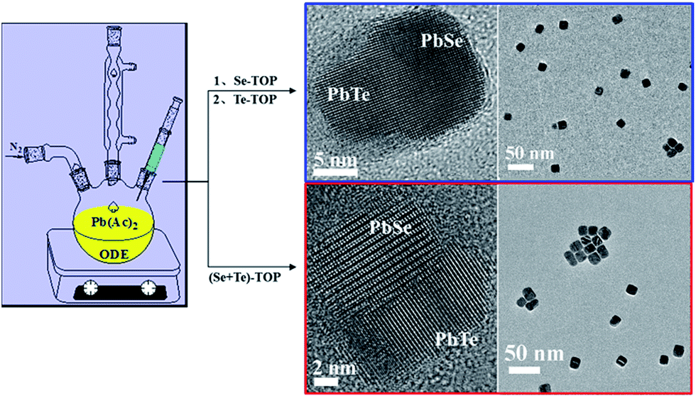 | ||
| Fig. 1 Schematic illustration of the formation of defect-free and defect-containing PbSe–PbTe HNPs. | ||
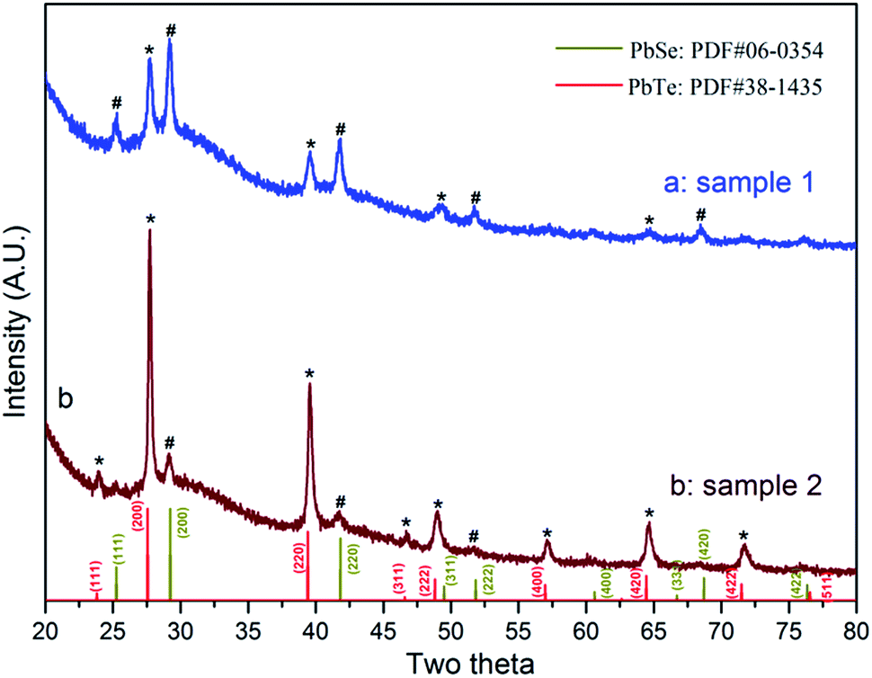 | ||
| Fig. 2 XRD patterns of the as-prepared defect-free and defect-containing PbSe–PbTe HNPs. | ||
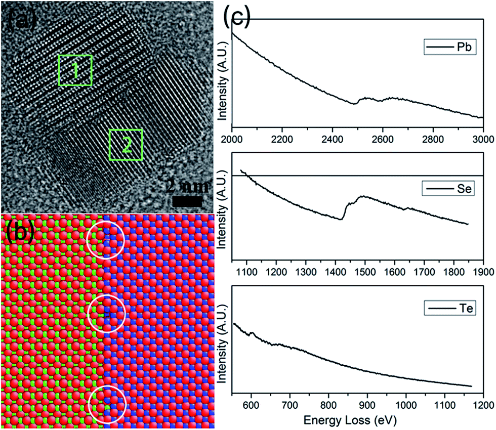 | ||
| Fig. 3 (a) HRTEM image of defect-containing PbSe–PbTe HNPs. (b) Possible atomic model corresponding to the defect-containing PbSe–PbTe HNPs showing defects in the interface. (c) EELS spectra of lead, selenium and tellurium edges taken from the areas marked 1 and 2 in (a). | ||
In order to analyse the defects or strain distribution at the heterojunction structure between PbSe and PbTe, the strain field surrounding the interface was measured by high-resolution TEM and applying the geometric phase-analysis (GPA) method. GPA enables a direct measurement of deformations at the atomic scale.33,34 Fig. 4a and c show typical phase contrast high-resolution TEM images containing lattice fringes with a typical interfacial boundary between PbSe and PbTe, respectively. Information about the strain field was extracted from these images using GPA, which is a lattice image processing method for semi-quantitative spatially distributed strain field analysis. Geometric phase analysis was used to investigate the variation in the lattice parameters and thus the strain at and around interfaces and boundaries. To reduce the potential artefacts of the strain analysis, it is necessary to obtain high-quality, clear lattice images. Fig. 4b and d show the shear strain map for the εyy component, clearly indicating compressive strain in the interface, which is periodically released at misfit dislocations. Fig. 4b and d present line profiles taken from PbSe to PbTe, which demonstrate the values of the strain in PbSe are higher than in PbTe. Fig. 4e presents a line profile taken across a dislocation core in the corresponding GPA map (Fig. 4d). A rapid decrease in the compressive εyy component is noticed when moving away from the interface in the PbSe–PbTe HNPs. This localized strain field shows a difference of ∼15% in the lattice parameters for the two phases, indicating that the most important deformation of the lattice is concentrated in two phases near the interface.
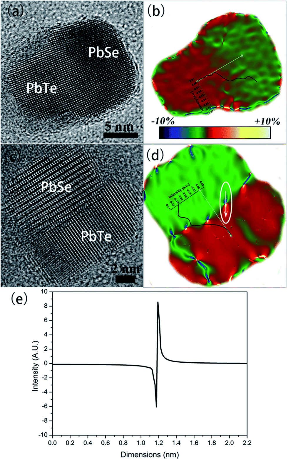 | ||
| Fig. 4 (a, c) HRTEM images of the defect-free and defect-containing PbSe–PbTe HNPs, respectively. (b, d) The εyy strain maps of the images in (a) and (c), respectively. (e) The line-scan profile of the region marked in (d). | ||
The electrical conductivity (σ), Seebeck coefficient (α) and power factor of the PbSe–PbTe HNPs mixed with PEDOT:PSS have been characterized. The data are listed in Table 1. Moreover, Fig. 5 displays the temperature dependence of electrical conductivity and Seebeck coefficient for the PbSe–PbTe HNPs. The Seebeck coefficient follows nearly linear temperature dependence up to 380 K and the room temperature Seebeck coefficients are around 17.7 and 18.8 μV K−1 for defect-containing PbSe–PbTe HNPs and defect-free PbSe–PbTe HNPs, respectively. The electrical conductivity values of the defect-containing and defect-free PbSe–PbTe HNPs are constant, but the value for the defect-containing PbSe–PbTe HNPs at ∼496 S m−1 is larger than that of the defect-free HNPs at ∼367 S m−1.
| Temperature (K) | Defect-free PbSe–PbTe HNPs | Defect-containing PbSe–PbTe HNPs | ||||
|---|---|---|---|---|---|---|
| σ (μV K−1) | α (S m−1) | Power factor (μW m−1 K−2) | σ (μV K−1) | α (S m−1) | Power factor (μW m−1 K−2) | |
| 293 | 18.8684 | 373.81093 | 0.13308 | 17.8243 | 500.10782 | 0.15889 |
| 312 | 19.5703 | 368.73658 | 0.14122 | 18.3384 | 494.72709 | 0.16638 |
| 328 | 20.0962 | 367.83532 | 0.14855 | 18.7354 | 493.90037 | 0.17337 |
| 345 | 20.3395 | 367.76114 | 0.15214 | 19.0369 | 493.32941 | 0.17878 |
| 360 | 20.6054 | 365.21388 | 0.15506 | 19.1452 | 495.45742 | 0.1816 |
| 376 | 20.9273 | 361.14785 | 0.15817 | 19.1795 | 498.14696 | 0.18324 |
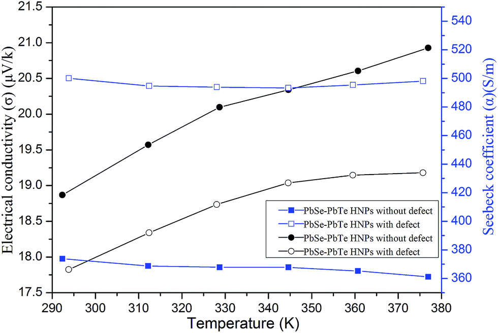 | ||
| Fig. 5 Temperature dependence of electrical conductivity (σ) and Seebeck coefficient (α) of the defect-free and defect-containing PbSe–PbTe HNPs. | ||
Fig. 6 shows the power factor (PF = α2σ) of the defect-containing and defect-free PbSe–PbTe HNPs, which represents the performance of the thermoelectric material. As the temperature increases, the power factor slowly increases for defect-containing and defect-free PbSe–PbTe HNPs. The maximum values of power factor for defect-containing and defect-free PbSe–PbTe HNPs are ∼0.183 and 0.158 μW m−1 K−2, respectively. These results demonstrate that the electrical conductivity and Seebeck coefficient can be manipulated by means of defects in the interface.
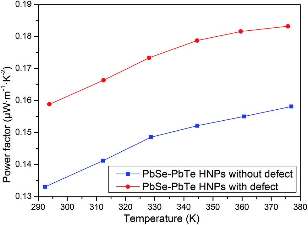 | ||
| Fig. 6 Temperature dependence of power factor of the defect-free and defect-containing PbSe–PbTe HNPs. | ||
4. Conclusions
In summary, we have developed a facile strategy to synthesize defect-containing and defect-free PbSe–PbTe HNPs, which was controlled by the addition of Se and Te precursors. The PbSe–PbTe heterojunction structure and detailed elemental distribution have been demonstrated by high-resolution TEM and EELS. Furthermore, the defects presenting in the interface of PbSe and PbTe have been directly imaged by GPA, confirming the existence of a strain system and a change in Seebeck coefficient and electrical conductivity data. The defects cause lattice distortion, changing the Seebeck coefficient, electrical conductivity and power factor, further modifying the thermoelectric properties of PbSe–PbTe HNPs. All the results suggest that this novel strategy may be a useful approach for tuning the thermoelectric properties of lead chalcogenides. Therefore, it has great potential in the application of flexible TE devices, and we will investigate the TE properties of the devices based on our as-prepared material in the future.Conflicts of interest
There are no conflicts to declare.Acknowledgements
This work was supported by the Ministry of Science and Technology of China (973 Project No. 2013CB932901), the National Natural Foundation of China (No. 51672050, 51725101, 11727807), and the scientific research start funding of the Shanghai Institute of Technology (39120K176003-YJ2016-3). This project was sponsored by the Shanghai Pujiang Program and “Shu Guang” project of the Shanghai Municipal Education Commission and Shanghai Education Development Foundation (09SG01).References
- L. E. Bell, Cooling, Heating, Generating Power, and Recovering Waste Heat with Thermoelectric Systems, Science, 2008, 321, 1457–1461 CrossRef CAS PubMed.
- Thermoelectrics and its Energy Harvesting, ed. D. M. Rowe, CRC Press, Boca Raton, FL, 2012 Search PubMed.
- S. I. Kim, K. H. Lee, H. A. Mun, H. S. Kim, S. W. Hwang, J. W. Roh, D. J. Yang, W. H. Shin, X. S. Li, Y. H. Lee, G. J. Snyder and S. W. Kim, Science, 2015, 348, 109 CrossRef CAS PubMed.
- L. D. Zhao, G. Tan, S. Hao, J. He, Y. Pei, H. Chi, H. Wang, S. Gong, H. Xu, V. P. Dravid, C. Uher, G. J. Snyder, C. Wolverton and M. G. Kanatzidis, Science, 2016, 351, 141 CrossRef CAS PubMed.
- A. I. Boukai, Y. Bunimovich, J. Tahir-Kheli, J. K. Yu, W. A. Goddard III and J. R. Heath, Silicon Nanowires as Efficient Thermoelectric Materials, Nature, 2008, 451, 168–171 CrossRef CAS PubMed.
- T. C. Harman, P. J. Taylor, M. P. Walsh and B. E. LaForge, Quantum Dot Superlattice Thermoelectric Materials and Devices, Science, 2002, 297, 2229–2232 CrossRef CAS PubMed.
- A. I. Boukai, Y. Bunimovich, J. Tahir-Kheli, J. K. Yu, W. A. Goddard III and J. R. Heath, Silicon Nanowires as Efficient Thermoelectric Materials, Nature, 2008, 451, 168–171 CrossRef CAS PubMed.
- L. D. Hicks and M. S. Dresselhaus, Effect of Quantum-Well Structures on the Thermoelectric Figure of Merit, Phys. Rev. B: Condens. Matter Mater. Phys., 1993, 47, 12727–12731 CrossRef CAS.
- L. D. Hicks, T. C. Harman, X. Sun and M. S. Dresselhaus, Experimental Study of the Effect of Quantum-Well Structures on the Thermoelectric Figure of Merit, Phys. Rev. B: Condens. Matter Mater. Phys., 1996, 53, 10493–10496 CrossRef.
- A. I. Hochbaum, R. K. Chen, R. D. Delgado, W. J. Liang, E. C. Garnett, M. Najarian, A. Majumdar and P. D. Yang, Enhanced Thermoelectric Performance of Rough Silicon Nanowires, Nature, 2008, 451, 163–165 CrossRef CAS PubMed.
- R. Venkatasubramanian, E. Siivola, T. Colpitts and B. O'Quinn, Thin-Film Thermoelectric Devices with High Room-Temperature Figures of Merit, Nature, 2001, 413, 597–602 CrossRef CAS PubMed.
- Y. Liu, M. Zhou and J. He, Towards higher thermoelectric performance of Bi2Te3 via defect engineering, Scr. Mater., 2016, 111, 39–43 CrossRef CAS.
- H. L. Tuller and S. R. Bishop, Point defects in oxides: tailoring materials through defect engineering, Annu. Rev. Mater. Res., 2011, 41, 369 CrossRef CAS.
- H. Wang, J. Zhang, X. Hang, X. Zhang, J. Xie, B. Pan and Y. Xie, Half-Metallicity in Single-Layered Manganese Dioxide Nanosheets by Defect Engineering, Angew. Chem., 2015, 127, 1211 CrossRef.
- Y. Lee, S.-H. Lo, J. Androulakis, C.-I. Wu, L.-D. Zhao, D.-Y. Chung, T. P. Hogan, V. P. Dravid and M. G. Kanatzidis, High-performance tellurium-free thermoelectrics: all-scale hierarchical structuring of p-type PbSeMSe systems (M = Ca, Sr, Ba), J. Am. Chem. Soc., 2013, 135(13), 5152–5160 CrossRef CAS PubMed.
- D. Parker, D. J. Singh, Q. Zhang and Z. Ren, Thermoelectric properties of n-type PbSe revisited, J. Appl. Phys., 2012, 111(12), 123701 CrossRef.
- X. Qian, L. Zheng, Y. Xiao, C. Chang and L.-D. Zhao, Enhancing thermoelectric performance of n-type PbSe via additional meso-scale phonon scattering, Inorg. Chem. Front., 2017, 4, 71–726 Search PubMed.
- Y. Zhou and M. Hu, Record Low Thermal Conductivity of Polycrystalline Si Nanowire: Breaking the Casimir Limit by Severe Suppression of Propagons, Nano Lett., 2016, 16, 6178–6187 CrossRef CAS PubMed.
- H. Dong, B. Wen, Y. Zhang and R. Melnik, Low Thermal Conductivity in Si/Ge Hereo-twinned superlattices, RSC Adv., 2017, 7, 29959–29965 RSC.
- W. Ma, J. M. Luther, H. Zheng, Y. Wu and A. P. Alivisatos, Photovoltaic devices employing ternary PbSxSe1-x nanocrystals, Nano Lett., 2009, 9, 1699–1703 CrossRef CAS PubMed.
- L. Etgar, D. Yanover, R. K. Čapek, R. Vaxenburg, Z. Xue, B. Liu, M. K. Nazeeruddin, E. Lifshitz and M. Grätzel, Core/Shell PbSe/PbS QDs TiO2 heterojunction solar cell, Adv. Funct. Mater., 2013, 23, 2736–2741 CrossRef CAS.
- Y. Zhang, Q. Dai, X. Li, J. Liang, V. L. Colvin, Y. Wang and W. W. Yu, PbSe/CdSe and PbSe/CdSe/ZnSe hierarchical nanocrystals and their photoluminescence, Langmuir, 2011, 27, 9583–9587 CrossRef CAS PubMed.
- K. T. Early and D. J. Nesbitt, Size-dependent photoionization in single CdSe/ZnS nanocrystals, Nano Lett., 2013, 13, 4844–4849 CrossRef CAS PubMed.
- D. Yanover, R. K. Čapek, A. Rubin-Brusilovski, R. Vaxenburg, N. Grumbach, G. I. Maikov, O. Solomeshch, A. Sashchiuk and E. Lifshitz, Small-sized PbSe/PbS core/shell colloidal quantum dots, Chem. Mater., 2012, 24, 4417–4423 CrossRef CAS.
- M. V. Kovalenko, R. D. Schaller, D. Jarzab, M. A. Loi and D. V. Talapin, Inorganically functionalized PbS-CdS colloidal nanocrystals: integration into amorphous chalcogenide glass and luminescent properties, J. Am. Chem. Soc., 2012, 134, 2457–2460 CrossRef CAS PubMed.
- T. Mokari, S. E. Habas, M. Zhang and P. Yang, Synthesis of lead chalcogenide alloy and core-shell nanowires, Angew. Chem., Int. Ed., 2008, 47, 5605–5608 CrossRef CAS PubMed.
- A. I. Hochbaum, R. Chen, R. D. Delgado, W. Liang, E. C. Garnett, M. Najarian, A. Majumdar and P. Yang, Nature, 2008, 451, 163–167 CrossRef CAS PubMed.
- Z. He, Y. Yang, J.-W. Liu and S.-H. Yu, Emerging tellurium nanostructures: controllable synthesis and their applications, Chem. Soc. Rev., 2017, 46, 2732–2753 RSC.
- G. Jeffrey Snyder and E. S. Toberer, Complex thermoelectric materials, Nat. Mater., 2008, 7, 105–114 CrossRef PubMed.
- Z. Zeng, P. Yang and Z. Hu, Temperature and size effects on electrical properties and thermoelectric power of bismuth telluride thin films deposited by co-sputtering, Appl. Surf. Sci., 2013, 268, 472–476 CrossRef CAS.
- M. He, J. Ge, Z. Lin, X. Feng, X. Wang, H. Lu, Y. Yang and F. Qiu, Thermopower Enhancement in Conducting Polymer Nanocomposites via Carrier Energy Scattering at the Organic-Inorganic Semiconductor Interface, Energy Environ. Sci., 2012, 5(8), 8351–8358 CAS.
- S. Butt, W. Xu, M. U. Farooq, G. K. Ren, Q. Zhang, Y. Zhu, S. U. Khan, L. Liu, M. Yu, F. Mohmed, Y. Lin and C.-W. Nan, Enhanced thermoelectricity in high-temperature β-phase copper (І) selenides embedded with Cu2Te nanoclusters, ACS Appl. Mater. Interfaces, 2016, 8, 15196–15204 CAS.
- M. J. Hytch, E. Snoeck and R. Kilaas, Ultramicroscopy, 1998, 57, 131 CrossRef.
- J. L. Rouvière and E. Sarigiannidou, Ultramicroscopy, 2005, 106, 1 CrossRef PubMed.
Footnote |
| † Electronic supplementary information (ESI) available. See DOI: 10.1039/c7ra09282b |
| This journal is © The Royal Society of Chemistry 2017 |