
 Open Access Article
 This Open Access Article is licensed under a
 Creative Commons Attribution 3.0 Unported Licence
Effects of GaxZn1−xO nanorods on the photoelectric properties of n-ZnO nanorods/p-GaN heterojunction light-emitting diodes
Rui Li ab,
Chunyan Yu*ab,
Hailiang Dongab,
Wei Jiaab,
Tianbao Liab,
Zhuxia Zhangab and
Bingshe Xuab
ab,
Chunyan Yu*ab,
Hailiang Dongab,
Wei Jiaab,
Tianbao Liab,
Zhuxia Zhangab and
Bingshe Xuab
aKey Laboratory of Interface Science and Engineering in Advanced Materials, Ministry of Education, Taiyuan University of Technology, Taiyuan 030024, China. E-mail: yuchunyan75@163.com
bResearch Center of Advanced Materials Science and Technology, Taiyuan University of Technology, Taiyuan 030024, China
First published on 25th October 2017
A Ga-doped ZnO nanorod array has been synthesized on a p-GaN/Al2O3 substrate by a hydrothermal method at low temperature. The structures and morphologies of the samples were measured by XRD and FE-SEM. The results show that the Ga-doped ZnO nanorods have excellent crystallinity and good epitaxial relationships with the substrate. With increasing Ga doping, the ZnO nanorods will grow along the [001] direction rapidly resulting in a decreasing average diameter. At the same time, the incorporation of Ga also significantly affects the optical and electrical properties of the n-ZnO nanorods/p-GaN heterojunction light-emitting diode. From the photoluminescence spectrum, it was found that Ga doping can be effectively regulated by the UV and visible emission peak intensity ratio of the ZnO nanorods. The I–V characteristics curve indicates that the n-ZnO nanorods/p-GaN heterojunction light-emitting diode will have better conductivity with increasing Ga doping concentration. Finally, the heterojunction light-emitting diode achieves green light emission under forward bias.1. Introduction
One-dimensional nanostructures such as nanorods (NRs) and nanowires (NWs) have been extensively studied,1–3 since their high crystallinity can provide an effective electron conduction path,4 and the vertical arrangement of NRs/NWs can also reduce the light of lateral scattering and enhance the light extraction efficiency,5,6 which makes it better than traditional planar p–n junction light-emitting diodes (LEDs).ZnO has wide application prospects in the fields of LEDs, LDs and solar cells because of its wide direct band gap (3.37 eV) and high exciton binding energy (60 meV) at room temperature.7–9 For the application of ZnO-based optoelectronic devices, it is necessary to fabricate both n-ZnO and p-ZnO. In recent years, although certain progress has been made in fabricating p-ZnO and even ZnO-based p–n homojunction LEDs, it is still difficult to prepare stable and reproducible high-quality p-type ZnO, which hinders the development of ZnO p–n homojunction LEDs.10,11 So far, many efforts have been devoted to developing ZnO-based p–n heterojunction LEDs with ZnO as the n-type layer, combined with other p-type layers, such as p-Si,12 p-GaN,13 p-AlGaN,14,15 and p-GaAs.16 Among them, it is important to explore a material that matches GaN, because both GaN and ZnO have the same crystal structure (hexagonal wurtzite), with a smaller lattice mismatch (1.8%) and with a similar room temperature wide band gap (3.4 eV).17,18
However, since the energy barrier of the n-ZnO/p-GaN junction interface leads to the low injection efficiency of carriers, the emission efficiency and output power of the heterojunction LED cannot meet the requirements of high performance devices.19 This problem can be improved by adding metal elements, such as Al, Ga, In and so on because these elements could form a doping level in the conduction band.
Ga doping can achieve smaller lattice distortions in GaxZn1−xO than Al or In doping under high doping concentrations because the bond length of Ga–O (1.92 Å) is closer to the bond length of Zn–O (1.97 Å) than that of Al–O (2.70 Å) or In–O (2.1 Å).20 Zehao et al. prepared Ga doped ZnO NR photodetectors with a smaller dark current and faster response speed by a low temperature hydrothermal method.21 He et al. synthesized individual heavily Ga-doped ZnO microwires via chemical vapor deposition methods, and bright, stable, and near-infrared light-emission from electrically biased individual Ga doped ZnO microwires was achieved.22 Studies have shown that Ga doping can significantly affect the growth behavior as well as the optical and electrical properties and defect states of ZnO NRs.23 Although there are a lot of reports on this issue, a disagreement still exists because the growth of NRs is sensitive to the doping concentration, reaction time, temperature and so on.24,25 In addition, little attention has been paid to the effect of Ga doping on the photoelectric properties of n-ZnO NRs/p-GaN heterojunction LEDs.
In this work, a Ga-doped ZnO NR array has been synthesized on a p-GaN/Al2O3 substrate. The effects of Ga doping concentration (0–3%) on the growth behaviour of ZnO NRs have been investigated and the photoelectric properties of the GaxZn1−xO NRs/p-GaN heterojunction LED are discussed.
2. Experimental
Ga-doped ZnO NRs were synthesized on p-GaN/Al2O3 (001) substrates by a low temperature hydrothermal growth process. The Mg-doped p-GaN film was grown on c-Al2O3 substrates using metal organic chemical vapor deposition. To grow more regular ZnO NRs on the p-GaN substrates, a ZnO seed layer was deposited on the substrate.26 The seed layer was then immersed in an aqueous solution containing a mixture of 0.075 M Zn(NO3)2·6H2O and equivalent molar hexamethylenetetramine (HMT, C6H12N4) at approximately 95 °C for 4.5 h. To obtain the Ga-doped samples, Ga(NO3)3·xH2O was added to the aqueous growth solution with nominal concentrations of 1 to 3 mol%. Hereafter, undoped ZnO and Ga-doped ZnO are denoted as UZO and GZO, respectively. To investigate the electrical properties of the heterojunction, Au electrodes were deposited onto the ZnO and GaN films by thermal evaporation. We first filled the gap of the nanorods with photoresist before depositing the electrodes to ensure that the electrode would have direct contact with the top of the nanorod. A schematic diagram of the structure of the heterojunction LED is shown in Fig. 1.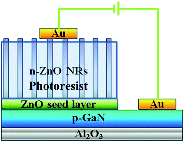 | ||
| Fig. 1 Schematic diagram of the structure of the heterojunction LED. | ||
The crystal structure of the sample was analyzed using a Japanese Y-2000 type X-ray diffractometer (Cu Kα ray, λ = 0.15418 nm), the morphology of the samples was analyzed by JEOL JSM6700F field emission scanning electron microscopy (FE-SEM), and the optical properties of the samples were analyzed by a Nanometrics Corporation NAN-RPM2000 Photoluminescence (PL) spectrometer (excitation wavelength: 266 nm). The electrical properties of the samples were tested with the FS-TL series LED test equipment.
3. Results and discussion
The influence of Ga doping on the structural properties of n-ZnO NRs was investigated by XRD and FE-SEM. Fig. 2 shows the XRD patterns of the n-ZnO NRs/p-GaN arrays with respect to the Ga doping concentration and its inset shows the enlarged view of the (002) peak. Strong diffraction peaks at 34.4° and 34.5° can be assigned to ZnO (002) and GaN (002) corresponding to JCPDS 36-1451 and JCPDS 50-0792, respectively. This indicates that all samples exhibit a wurtzite hexagonal structure regardless of the growth conditions. Beyond that, the (002) diffraction peaks of all samples are sharp and the NRs have a [001] growth direction, indicating that the ZnO NRs have excellent crystallinity and a good epitaxial relationship with the p-GaN epitaxial film. No additional peak related either to Ga or its oxides was detected, which indicates that the Ga atoms have been solid-solved into the interior of the ZnO lattice. As can be seen in the enlarged view of the (002) peaks, the ZnO (002) peak position does not show obvious displacement with the increase of the Ga doping concentration, indicating that Ga doping does not cause lattice mismatch.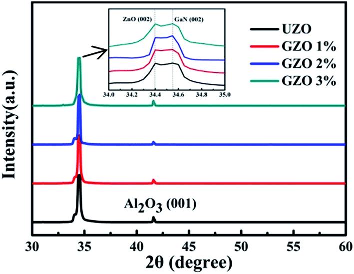 | ||
| Fig. 2 XRD patterns of the ZnO NR arrays with different Ga doping concentrations. The inset shows the enlarged view of the (002) peak. | ||
Fig. 3(a)–(d) exhibit the plan-view SEM images of the morphologies of the UZO and GZO NRs, and Table 1 presents the distribution of the different elements (Zn, O and Ga) in the UZO and GZO NRs detected by EDS. For all samples, the hexagonal-shaped NRs were vertically grown on the p-GaN film, which is consistent with the XRD results. The average diameter and the number of NRs per unit estimated from the corresponding SEM images are plotted in Fig. 3(e). It can be seen intuitively that the average diameter and the density both decrease as the Ga concentration increases. In addition, the uniformity of the NRs deteriorates with increasing doping concentration. It has been reported that the ZnO NRs will grow along the [001] direction rapidly with Ga doping, thus there is a decrease in the average diameter.27 Moreover, the incorporation of Ga ions inhibits the formation of the ZnO nuclei,21 so the density of the NRs decreases with increasing Ga doping concentration. These results demonstrate that the growth behavior of the ZnO NRs is significantly affected by Ga doping. The comparison of the EDS data with different doping concentration shows that with an increase in doping concentration, the ratio of Ga to Zn in the ZnO NRs increases, indicating that Ga atoms have been incorporated into the ZnO NRs effectively.
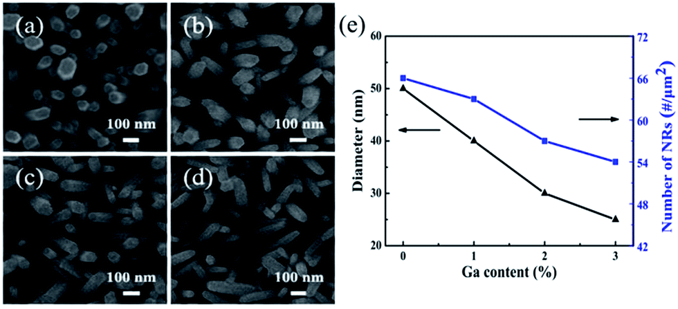 | ||
| Fig. 3 Plan-view FE-SEM images of the GZO NRs with different Ga concentrations: (a) 0%, (b) 1%, (c) 2%, and (d) 3%, and (e) variations of the average diameter and density. | ||
| UZO | GZO 1% | GZO 2% | GZO 3% | |
|---|---|---|---|---|
| Zn atomic percent | 55.3% | 55.1% | 53.4% | 48.2% |
| Ga atomic percent | 0% | 0.2% | 0.4% | 0.7% |
| Ga/(Ga + Zn) ratio | 0% | 0.4% | 0.7% | 1.4% |
Fig. 4 depicts the photoluminescence spectra of p-GaN (a) and n-ZnO NRs/p-GaN with different Ga doping concentrations (b). p-GaN has a relatively sharp UV emission peak at 360 nm. Fig. 4(b) shows two emission peaks for all samples: a strong UV emission peak located at 358 nm and an almost negligible visible emission peak at about 620 nm. The UV emission peak is attributed to the recombination of free excitons through a near band edge exciton–exciton collision process, and the visible emission peak is associated with the electron–hole recombination at deep levels caused by intrinsic defects such as oxygen vacancies and/or zinc interstitials.21 In this experiment, the low intensity of the defect emission peak indicates that the prepared ZnO NRs have good crystallinity and excellent optical efficiency. A similar result was obtained by Rogers et al.28 They reported a ZnO/GaN p–n heterojunction LED using a pulsed laser, and the PL showed a main peak at 375 nm and a negligibly low green emission. With increasing Ga doping concentration, the intensity of the UV peak of the ZnO NRs first increases and then decreases, reaching a maximum peak in the GZO 1% sample. The illustration in Fig. 4(b) is a visible emission peak magnified 50×, and its intensity decreases with the increase of Ga doping. It is generally believed that the ratio of the UV peak to the visible emission peak is related to the crystal quality of the sample: the larger the ratio, the higher the crystal quality. Therefore, when the Ga doping concentration is 1%, the sample has the best crystalline quality, which is in agreement with the XRD results. When the Ga doping content increases further, the UV peak intensity reduces because of the introduction of more nonradiative recombination centers. Therefore, the incorporation of Ga can affect the crystal quality of ZnO. Beyond that, there was a small redshift of the peak in the UV emission, which can be ascribed to the Ga-doping induced band gap renormalization effect.29
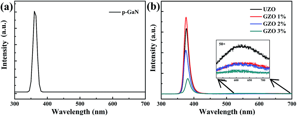 | ||
| Fig. 4 Photoluminescence spectra of the p-GaN (a) and the n-ZnO NRs with different Ga doping concentrations (b). | ||
Fig. 5 exhibits the I–V characteristics of the ZnO NRs/p-GaN heterojunction with different Ga doping concentrations. The inset shows the I–V characteristics of Au/GaN and Au/ZnO, indicating that there is good ohmic contact between the electrode and the material. p-GaN acts not only as a ZnO NR buffer layer, but also as a p-type hole injection layer. And the hole concentration of the p-GaN is about 4.0 × 10¹⁷. The curves of all samples show rectification characteristics. The current increases with increasing voltage and at the same forward bias, the higher the Ga doping concentration, the greater the current of the heterojunction. This phenomenon indicates that the electrical conductivity of the ZnO NRs increases with the increase of the Ga content. This is because the increasing Ga doping concentration results in the number of carriers (electrons) increasing in the ZnO NRs, thus reducing the resistance of the heterojunctions.
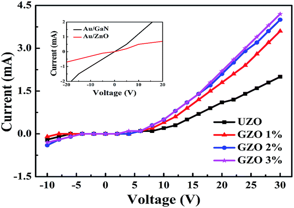 | ||
| Fig. 5 I–V characteristics of the n-ZnO NRs/p-GaN heterojunction LED with different Ga doping concentrations. The inset shows the I–V characteristics of Au/ZnO and Au/GaN. | ||
It is observed that the heterojunction LED luminescence is on the ZnO side when a forward bias is applied. Fig. 6(a) shows the electroluminescence spectra of the 1% GZO nanorods/p-GaN heterojunction when the bias voltage is 30 V (a) and the emission peak is centered at 520 nm at a reverse bias voltage of 30 V. Fig. 6(b) is the CIE 1931 color coordinate measurement for the heterojunction LEDs at 30 V when the Ga doping content is 1%, and the chromaticity coordinate is (0.3228, 0.4591). As the image illustrates in the inset of Fig. 6(b), the EL emission is clearly seen by the naked eye. Similar results for the light emission of an n-ZnO NRs/p-GaN heterojunction LED have been reported. Fu et al. demonstrated a ZnO NRs/p-GaN heterojunction LED, and observed green emission centered at 519 nm at a reverse bias voltage of 3.5 V that originated from oxygen vacancies near the heterojunction interface.30 The origin of the EL emissions can be determined from the energy band diagram shown in Fig. 7, combined with the photoluminescence spectra of the p-GaN and the n-ZnO NRs/p-GaN with different Ga doping concentrations as shown in Fig. 4.
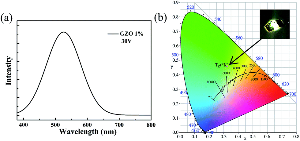 | ||
| Fig. 6 Electroluminescence spectra of the 1% GZO nanorods/p-GaN heterojunction when the bias voltage is 30 V (a) and the chromaticity coordinates of the light emission from the LED operated at 30 V (b). The inset of (b) shows the image of the device at the corresponding voltage. | ||
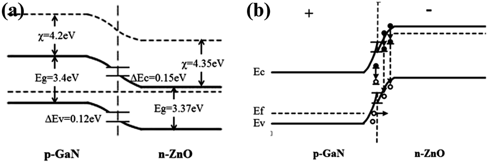 | ||
| Fig. 7 The energy band diagram of the n-ZnO NRs/p-GaN heterojunction without applying a voltage (a) and applying forward bias (b). | ||
The electron affinities of ZnO (χZnO) and GaN (χGaN) are 4.35 and 4.2 eV. The conduction band offset is ΔEc = χZnO − χGaN = 0.15 eV, and the valence band offset is ΔEv = Eg ZnO + ΔEc − Eg GaN = 0.12 eV, according to the Anderson model. Although the electron mobility is greater than that of the hole, the holes in p-GaN are more likely to be implanted into ZnO due to the fact that the barrier of the holes is smaller than that of the electrons and the depth of the depletion layer required for the holes is much smaller than that of the electrons. When a forward bias is applied, the electrons injected into the ZnO conduction band are easily occupied by the low-energy electrons associated with the defects, and are recombined with the holes injected from GaN into the ZnO valence band and into ZnO intrinsic holes.
4. Conclusions
A GaxZn1−xO NRs/p-GaN heterojunction LED has been fabricated. Test results show that Ga doping can significantly affect the growth behavior of ZnO NRs and the photoelectric properties of the n-ZnO NRs/p-GaN heterojunction LED. When the Ga doping concentration is 1%, the crystal quality and optical properties of the sample are optimal. Heterojunction LEDs have better conductivity with the increase of Ga doping concentration. A strong green emission is obtained when the Ga doping concentration is 1%. The origin of the EL emission is supposed to be attributed to the defects in the heterojunction combined with an energy band structure diagram. This method provides a meaningful approach for the preparation of ZnO-based optoelectronic devices achieving excellent performance.Conflicts of interest
There are no conflicts to declare.Acknowledgements
This work is financially supported by the National Natural Science Foundation of China (Grant no. 21471111, 61475110, 61404089, 61504090 and 61604104), the Natural Science Foundation of Shanxi Province (Grant no. 2014011016-6 and 2015011034), the Basic Research Projects of Shanxi Province (Grant no. 2015021103) and the Shanxi Provincial Key Innovative Research Team in Science and Technology (Grant no. 201605D131045-10).References
- Z. Liang, X. Cai and S. Tan, et al., Phys. Chem. Chem. Phys., 2012, 14, 16111–16114 RSC.
- X. W. Sun, J. Z. Huang and J. X. Wang, et al., Nano Lett., 2008, 8, 1219–1223 CrossRef CAS PubMed.
- Y. Zhang, D. Q. Fang and S. L. Zhang, et al., Phys. Chem. Chem. Phys., 2016, 18, 3097–3102 RSC.
- Y. J. Lee, Z. P. Yang and F. Y. Lo, et al., Apl Materials, 2014, 2(5), 42 CrossRef.
- H. Jeong, D. J. Park and H. S. Lee, et al., Nanoscale, 2014, 6, 4371–4378 RSC.
- B. U. Ye, B. J. Kim and Y. H. Song, et al., Adv. Funct. Mater., 2012, 22, 632–639 CrossRef CAS.
- Ü. Özgür, Y. I. Alivov and C. Liu, et al., J. Appl. Phys., 2005, 98, 11 CrossRef.
- C. Bayram, F. Hosseini Teherani and D. J. Rogers, et al., Appl. Phys. Lett., 2008, 93, 459 Search PubMed.
- X. N. Wang, Y. Wang and Z. X. Mei, et al., Appl. Phys. Lett., 2007, 90, 2720 Search PubMed.
- C. Klingshirn, ChemPhysChem, 2007, 8(6), 782 CrossRef CAS PubMed.
- D. C. Look, B. Claflin and Y. I. Alivov, et al., Phys. Status Solidi, 2004, 201, 2203–2212 CrossRef CAS.
- G. Xiong, J. Wilkinson and S. Tuzemen, et al., Proc. SPIE, 2011, 4644, 256–262 CrossRef.
- Y. I. Alivov, J. E. Van Nostrand and D. C. Look, et al., Appl. Phys. Lett., 2003, 83, 2943–2945 CrossRef CAS.
- Q. X. Yu, B. Xu and Q. H. Wu, et al., Appl. Phys. Lett., 2003, 83, 4713–4715 CrossRef CAS.
- Y. I. Alivov, E. V. Kalinina and A. E. Cherenkov, et al., Appl. Phys. Lett., 2003, 83, 4719–4721 CrossRef CAS.
- S. E. Nikitin, Y. A. Nikolaev and V. Y. Rud, et al., Semiconductors, 2004, 38, 393–396 CrossRef CAS.
- T. P. Yang, H. C. Zhu and J. M. Bian, et al., Mater. Res. Bull., 2008, 43, 3614–3620 CrossRef CAS.
- S. Fiatvarol, D. Sahin and M. Kompitsas, et al., RSC Adv., 2014, 4, 13593–13600 RSC.
- S. K. Hong, T. Hanada and H. Makino, et al., Appl. Phys. Lett., 2001, 78, 3349–3351 CrossRef CAS.
- S. J. Young, C. L. Chiou and Y. H. Liu, et al., Inventions, 2016, 1, 3 CrossRef.
- S. Zehao, Z. Hai and Y. Cong, et al., Mater. Sci. Semicond. Process., 2017, 64, 101–108 CrossRef.
- G. H. He, M. M. Jiang and L. Dong, et al., J. Mater. Chem. C, 2017, 5, 2542–2551 RSC.
- G. C. Park, S. M. Hwang and J. H. Lim, et al., Nanoscale, 2014, 6, 1840–1847 RSC.
- G. Pineda-Hernández, A. Escobedo-Morales and U. Pal, et al., Mater. Chem. Phys., 2012, 135, 810–817 CrossRef.
- J. Guo, J. Zheng and X. Song, et al., Mater. Lett., 2013, 97, 34–36 CrossRef CAS.
- T. A. N. Peiris, H. Alessa and J. S. Sagu, et al., J. Nanopart. Res., 2013, 15, 2115 CrossRef.
- J. Joo, B. Y. Chow and M. Prakash, et al., Nat. Mater., 2011, 10, 596 CrossRef CAS PubMed.
- D. J. Rogers, F. H. Teherani and A. Yasan, et al., Appl. Phys. Lett., 2006, 88, 58 CrossRef.
- P. Y. Yang, H. Wang and X. N. Wang, et al., J. Nanosci. Nanotechnol., 2011, 11, 10804–10808 CrossRef CAS PubMed.
- Q. M. Fu, W. Cao and G. W. Li, et al., Appl. Surf. Sci., 2014, 293, 225–228 CrossRef CAS.
| This journal is © The Royal Society of Chemistry 2017 |