
 Open Access Article
 This Open Access Article is licensed under a
 Creative Commons Attribution 3.0 Unported Licence
CuO/V2O5 hybrid nanowires for highly sensitive and selective H2S gas sensor†
Bu-Yu Yeha,
Bo-Sung Jiana,
Gou-Jen Wang b and
Wenjea J. Tseng*a
b and
Wenjea J. Tseng*a
aDepartment of Materials Science and Engineering, National Chung Hsing University, Taichung 402, Taiwan. E-mail: wenjea@dragon.nchu.edu.tw
bDepartment of Mechanical Engineering, National Chung Hsing University, Taichung 402, Taiwan. E-mail: gjwang@dragon.nchu.edu.tw
First published on 25th October 2017
Abstract
Vanadium pentoxide (V2O5) nanowires decorated with CuO nanoparticles on their surface have been prepared by a facile chemical route. The gas-sensing performance of the CuO/V2O5 nanohybrids has been examined against H2S, CO, and NO2 gases over a range of gas concentrations from 7 to 60 ppm and working temperatures from 100 to 400 °C, and compared with that of pristine V2O5 nanowires without the decoration. The CuO/V2O5 nanohybrids exhibit a greatly enhanced sensitivity toward H2S gas selectively and are relatively indifferent to CO and NO2 gases. The gas-sensing response of the nanohybrids increases by nearly 18 times (from 1.84 to 31.86) when tested against 23 ppm of H2S gas at 220 °C. The nanohybrids remain stable when detecting H2S gas for a period of two weeks. This selective enhancement is attributable to the local p–n junction formed at the interface together with the reversible chemical reaction that occurs when CuO is exposed to H2S gas at the temperature employed.
Introduction
Hydrogen sulphide (H2S) is a “broad-spectrum” poison, namely it is toxic to several systems in the human body, however the nerve system is most affected. Enzymes that exist in the human body are capable of detoxifying H2S by oxidation to harmless sulfates. However, the oxidative enzymes become overwhelmed when the H2S concentration exceeds a certain threshold level of about 300–350 ppm on average.1 To avoid harmful incidents occurring, the design of commercial H2S gas sensors capable of detecting minute gas concentrations at ppm levels often requires a detection level as low as 5–15 ppm under moderate working temperatures. In this regard, chemiresistor-type sensors based on one-dimensional metal oxide semiconductors (MOSs) are attractive since they are capable of providing gas-sensing ability for the stable detection of trace amounts of hazardous gases with a wide range of chemical attributes. To detect H2S gas specifically, various MOS sensing materials such as WO3, SnO2, ZnO, In2O3 and CuO have been explored.2 The MOS sensors still suffer from major drawbacks such as cross-sensitivity, sensitivity to humidity, long-term signal drifting and slow sensor response.3 In particular, the poor selectivity remains a challenge to overcome and often limits their practical applicability.2–4In the literature, the gas-sensing properties of one-dimensional n-type vanadium pentoxide (V2O5) has seldom been addressed, despite its promising potential in gas detection.5–10 Liu et al. first prepared V2O5 nanobelts decorated with either Fe2O3, TiO2 or SnO2 nanoparticles by a hydrothermal method.5,6 The hybrid nanobelts showed a moderately enhanced sensing response (S = 2.0–3.1 at 100 ppm ethanol) when compared to the pristine V2O5 nanobelts (S = 1.7) at 200 °C. Since then, V2O5 nanostructures have been investigated as gas sensors for detecting mostly organic vapours.7–10 Among them, Raible et al. reported a high sensitivity against organic amines such as 1-butylamine, with a detection limit as low as 30 ppb using V2O5 nanofibres.7 Raj et al. chemically prepared V2O5 nanostructures and found that V2O5 showed a slightly improved sensitivity toward ethanol at ppm levels compared to ammonia with identical concentrations at room temperature.8,9 Mondaferri et al. also demonstrated the sensing response against ammonia gas over a concentration range of 0.85–8.5 ppm at 200–250 °C using electrospun V2O5 nanofibres.10 Recently, the use of V2O5 nanostructures for the detection of inorganic, hazardous gases has begun to emerge.11–13 Yan et al. reported the room-temperature sensing capability of a porous silicon/V2O5 nanorod composite with a selective, substantially enhanced sensitivity toward NO2 gas at low concentrations (3 ppm). This compares favourably to that of organic gases such as ethanol, methanol and acetone with an even higher concentration (100 ppm).11 Mane et al. prepared V2O5 and Pd-decorated V2O5 nanorods on glass substrates by chemical spraying and subsequent thermal treatment.12,13 They also found an enhanced selectivity against NO2 gas compared to other gases including NH3, H2S, CO, and SO2.13
The use of V2O5 nanostructures as sensors for detecting inorganic toxic gases requires more work to assess their applicability. We herein report the decoration of CuO nanoparticles onto V2O5 nanowires to form hybrid nanostructures and investigate the gas sensitivity/selectivity of these nanostructures toward the toxic gases H2S, CO and NO2. The reason for selecting CuO for the hybrid structure lies in the fact that there are reports about enhanced selective sensing achieved with p-type CuO semiconductors exposed to H2S gas.14–17 For the first time, the CuO/V2O5 nanohybrids have been found to exhibit highly sensitive and selective detection toward H2S gas at ppm levels continuously over a prolonged period of time (up to two weeks) and are relatively indifferent to CO and NO2 gases over the moderate temperature range examined.
Results and discussion
Fig. 1(a) shows the morphology of the hydrothermally prepared V2O5 nanowires. V2O5 nanowires with a uniform diameter of 100 to 250 nm, a length of 10 to 20 μm and a smooth topography have been obtained. The XRD pattern in Fig. 1(b) shows characteristic diffraction peaks in good agreement with those of the orthorhombic V2O5 structure (JCPDS no. 41-1426). Fig. 2 shows that the V2O5 nanowires are of single crystal morphology. The lattice-fringe spacings in Fig. 2(b) are 0.434 and 0.343 nm, corresponding to the (001) and (110) planes of orthorhombic V2O5, respectively. The nanowires grow along the [110] direction preferentially.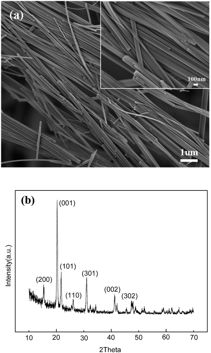 | ||
| Fig. 1 (a) FE-SEM image and (b) XRD pattern of the hydrothermally prepared V2O5 nanowires. | ||
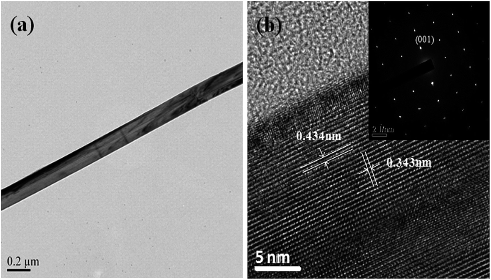 | ||
| Fig. 2 (a) Bright-field TEM image, (b) HRTEM image and SAED pattern (inset) of a single V2O5 nanowire. | ||
The V2O5 nanowires served as a backbone for the preparation of CuO/V2O5 hybrids with decorative CuO nanoparticles. Fig. 3(a) shows that the CuO nanoparticles with a diameter of about 50 nm are well dispersed on the V2O5 surface. Fig. 3(b) shows a typical TEM bright-field image of the CuO/V2O5 hybrids, in which discrete CuO nanoparticles seem to adhere onto the V2O5 surface. The black dots are monoclinic CuO which was verified by TEM (Fig. S1 in the ESI†). Fig. 3(c) displays an XRD pattern of the CuO/V2O5 hybrids prepared via a deposition process, with a heat-treatment temperature of 400 °C. Well-defined crystalline phases have been found for the orthorhombic V2O5 and monoclinic CuO (JCPDS no. 48-1548), without the formation of any intermediate alloying compounds. It is worthwhile to note that the heat-treatment temperature turned out to be critically important for the successful preparation of CuO/V2O5 hybrids. If the temperature was raised to 500 °C, the hybrids became irregular fragments as shown in Fig. 3(d), suggesting that the V2O5 nanowires had partially melted or softened (note that the melting temperature of pure bulk V2O5 is about 690 °C) so the structure of the hybrid was destroyed.
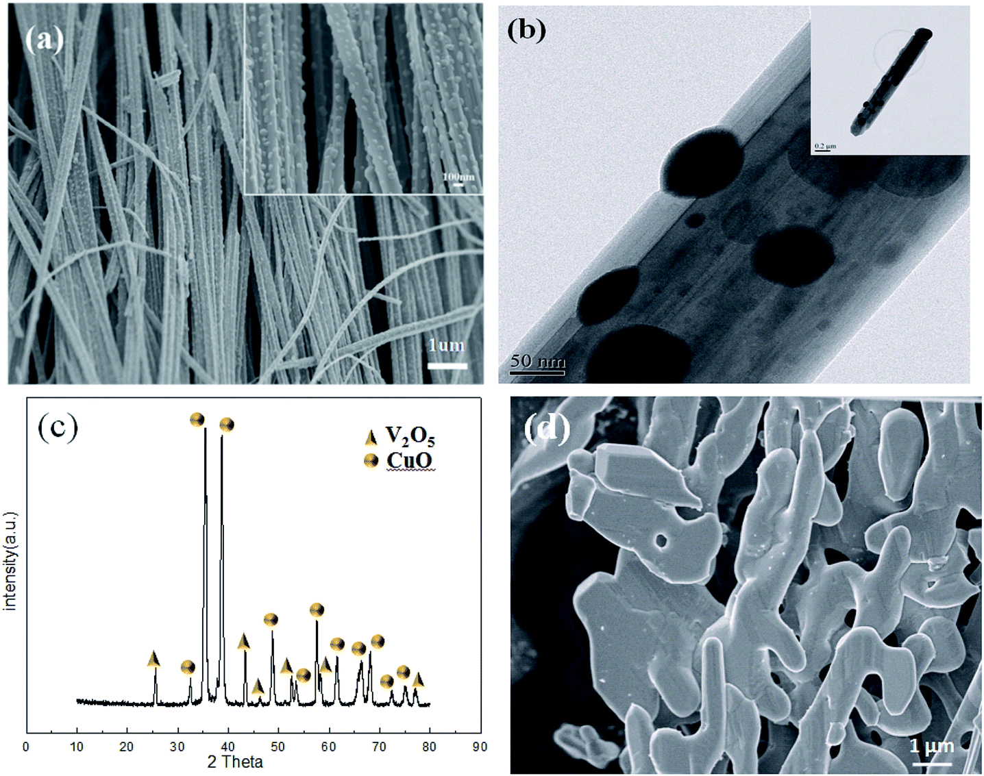 | ||
| Fig. 3 (a) FE-SEM, (b) bright-field TEM and (c) XRD pattern of the CuO/V2O5 hybrids prepared at 400 °C. (d) FE-SEM image of the CuO/V2O5 hybrids prepared at 500 °C. | ||
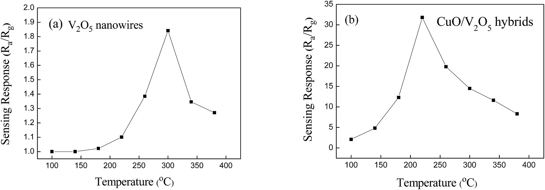
Fig. 4 shows the sensing response of the pristine V2O5 and the CuO/V2O5 hybrid nanowires against 23 ppm H2S gas over a temperature range from 100 to 380 °C. Two important findings have been observed. Firstly, the bell-shaped distribution reveals an optimum working temperature at which the sensing response is highest. This bell-shaped temperature dependence is ascribed to two main reasons.17 On the one hand, the adsorption, desorption and diffusion reactions involved, between the target gas and the semiconducting oxide surface, are all thermally activated processes. Hence the response increases with the working temperature.3 On the other hand, electrons in oxide semiconductors are more likely to attain sufficient energy to jump to the conduction band from the valence band at elevated temperatures. This leads to an increased concentration of free electrons so that electrical resistance is reduced accordingly. A combination of the thermally activated process, together with the increased probability of free-electron formation as the temperature was increased, results in an optimal temperature at which the electrical resistance (and hence the sensing response) is highest. In this regard, we have demonstrated for the first time that the optimal sensing temperature can be tailored to a lower temperature, against the model H2S gas at ppm levels, through the decoration of CuO nanoparticles onto V2O5 nanowires in Fig. 4. Secondly, we have found that the CuO/V2O5 hybrids show a response as high as 31.86 against H2S gas at ppm levels at 220 °C. For the first time, this compares favourably with that of the pristine V2O5, for which the highest response is merely 1.84 at 300 °C. The increased sensitivity is ascribed to the hybridization of V2O5 with the CuO nanoparticles together with the decorative hybrid structure, and will be discussed in later sections.
 | ||
| Fig. 4 Gas-sensing response of the (a) pristine V2O5 nanowires and (b) CuO/V2O5 hybrids against 23 ppm H2S over a broad temperature range. | ||
The CuO/V2O5 hybrid nanowires also display a significantly enhanced gas selectivity which is highly desirable in practical sensing applications. To illustrate this, the dynamic resistance behaviour of the pristine V2O5 nanowires is displayed in Fig. 5 against H2S, CO, and NO2 gases at 300 °C. Responses of the V2O5 nanowires are 1.84 for 23 ppm H2S gas, 1.48 for 60 ppm CO gas and 1.46 for 30 ppm NO2 gas.
 | ||
| Fig. 5 Dynamic resistance change of the pristine V2O5 nanowire sensors against (a) H2S, (b) CO and (c) NO2 gases, at ppm-level concentrations at 300 °C. (d) A summary of the responses of the V2O5 nanowires against H2S, CO, and NO2 gas at 300 °C. | ||
In addition, the response times toward detection of H2S, CO, and NO2 gases are 196, 174, and 212 s, respectively, as shown in Fig. 6(a–c), for the above gas concentrations. The sensing properties are primarily ascribed to the exchange of charge carriers between the adsorbed gas molecules and the V2O5 surface. In an air atmosphere, chemisorbed oxygen species, such as O2−, O− and O2−, trap electrons from the conduction band of the n-type V2O5 semiconductor, resulting in a space-charge depletion near the surface.18 After the introduction of the reducing H2S or CO gas into the testing chamber, the gas molecules would react with the previously chemisorbed oxygen ions, so that the electrons trapped by the absorbed oxygen would subsequently be released into the bulk V2O5 nanowires, according to the following reactions (1) and (2):
| 4H2S + 6O2−(ads) → 4SO2 + 4H2O + 6e− | (1) |
| 2CO + O2−(ads) → 2CO2 + e− | (2) |
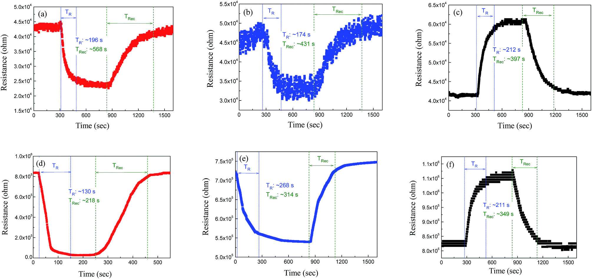 | ||
| Fig. 6 Response time (TR) and recovery time (TRec) of the pristine V2O5 nanowires against (a) H2S (23 ppm), (b) CO (60 ppm) and (c) NO2 (30 ppm) at 300 °C, respectively. TR and TRec of the CuO/V2O5 hybrid nanowires against (d) H2S (23 ppm), (e) CO (60 ppm) and (f) NO2 (30 ppm) at 220 °C, respectively. | ||
This produces free electrons and hence decreases the electrical resistance. When the reducing gases were removed from the atmosphere, oxygen molecules spontaneously adsorb onto the V2O5 surface reversibly to trap free electrons, which causes the electrical resistance to increase, returning back to its initial value. In contrast, the adsorption of oxidizing NO2 gas would deplete the number of charge carriers in the surface layer of the V2O5 nanowires. This widens the depletion region, resulting in an increase in the electrical resistance accordingly. The desorption of gas molecules from the pristine V2O5 appears to be more difficult than the adsorption, so that a “tail” was found in Fig. 6(a–c).
In addition, Fig. 5(d) summarizes the sensing response of the pristine V2O5 nanowires. The lack of gas selectivity is apparent, however the sensor does provide a decent response to a change in concentration of the target gases over ppm concentrations, examined at the given working temperature.
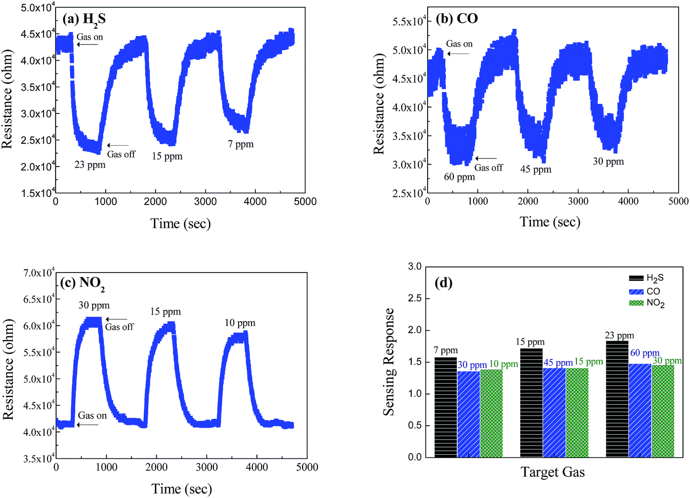
Fig. 7 shows the dynamic resistance change of the CuO/V2O5 hybrids against H2S, CO, and NO2 gases. The responses of the hybrids are 1.33 against 60 ppm CO gas, and 1.29 against 30 ppm NO2 gas at 220 °C. The result resembles that of the pristine V2O5 nanowires at 300 °C, despite the fact that the sensing temperature employed was reduced. A significantly enhanced sensing performance was found for the CuO/V2O5 hybrids toward H2S gas selectively. Fig. 7(a) shows the resistance change of the CuO/V2O5 hybrids against H2S gas of various concentrations at 220 °C; the responses are 31.86 at 23 ppm, 20.89 at 15 ppm and 7.86 at 7 ppm. This result indicates a dramatic enhancement of the sensing response from 1.84 for the pristine V2O5 nanowires to 31.86 for the CuO/V2O5 hybrids upon exposure to 23 ppm H2S. Compared to the rather indifferent sensitivity of the hybrid nanowires against CO and NO2 gases, a significantly increased sensing performance, nearly 18 times that of the pristine V2O5 nanowires, has been discovered toward H2S gas selectively over the various gases and gas concentrations examined, as summarized in Fig. 8. Not to mention the fact that this occurs at a slightly lower working temperature (220 °C). In addition, Fig. 6(d) shows that the response time of the hybrid is 130 s for H2S gas at a 23 ppm concentration. Therefore, the enhanced selective sensitivity is obtained with a simultaneously shortened response time. In comparison, the response times to detect CO and NO2 gases are 268 and 211 s for the hybrids, respectively, which are similar to that of the pristine counterpart. Similar results have been found for the recovery times. The detection limit of the hybrid CuO/V2O5 nanowires has been determined experimentally, in which no response was detectable when the H2S concentration was below 3 ppm.
 | ||
| Fig. 7 Dynamic resistance change of the CuO/V2O5 hybrids against (a) H2S, (b) CO and (c) NO2 at ppm-level concentrations at 220 °C. (d) A summary of the gas response of the CuO/V2O5 hybrids against H2S, CO and NO2 at 220 °C. | ||
 | ||
| Fig. 8 Selectivity of V2O5 nanowires and CuO/V2O5 hybrids toward H2S, CO and NO2 gases at the optimal working temperature (300 °C for V2O5, 220 °C for CuO/V2O5). | ||
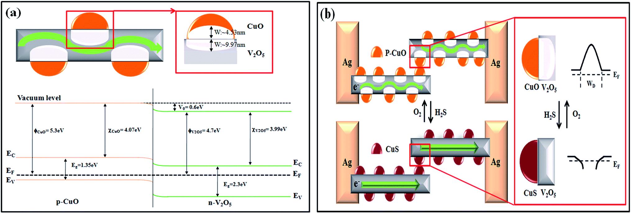
The selective enhancement and increased sensitivity toward H2S gas sensing of the CuO/V2O5 hybrids may be explained by the p–n junction formed at the dissimilar interface and sulfuration of the decorative CuO. The intrinsic V2O5 and CuO are n- and p-type semiconductors, respectively. The decoration of CuO onto V2O5 in the hybrids forms local p–n junctions at the interface.14–17,19,20 The width of the space-charge region (W) at the interface can be estimated from eqn (3) and (4) for n-V2O5 and p-CuO, respectively:20,21
 | (3) |
 | (4) |
where ε is the permittivity (2.25 × 10⁻¹¹ F m−1 for V2O5 and 2.123 × 10⁻¹⁰ F m−1 for CuO),20,22 Vo (= 0.6 eV) is the contact potential which is equal to the amount of the energy band bending between V2O5 and CuO (ϕCuO − ϕV2O5), q is the electrical charge of the carrier (1.6 × 10⁻¹⁹ C), and N is the carrier concentration (NV2O5 = 1.48 × 1018 cm−3 and NCuO = 1 × 1019 cm−3, at room temperature).20,23 The calculated space-charge widths are 9.97 nm for V2O5 and 4.53 nm for CuO. These estimates are used for the plot of the energy-band diagram of CuO/V2O5 p–n junction in air and H2S, in Fig. 9(a). Energy-band bending at the interface is apparent. The band gap (Eg), electron affinity (χ) and work function (ϕ) of V2O5 are 2.3, 3.99, and 4.7 eV, respectively.24,25 Those of CuO are 1.35, 4.07, and 5.3 eV, respectively.20 Note that the calculated space-charge widths are an estimate since the carrier concentrations used in the calculation are the values at room temperature. A more precise determination of the WV2O5 and WCuO needs information about the carrier concentrations at the working temperature (220 °C) employed. Nonetheless, the electrical transport channel is suppressed by the presence of local p–n junctions, according to the estimates of the space-charge region. This would hence lead to a higher base resistance (as observed in Fig. 6 where the base resistance values of the CuO/V2O5 hybrids were 10 to 20 times greater than that of the pristine V2O5) and a larger change in electrical resistance (and hence sensing response) for the CuO/V2O5 hybrid nanowires compared to that of the pristine V2O5 counterpart.
 | ||
| Fig. 9 (a) The band bending diagram and depletion-layer width at the p–n junction. (b) The energy-band diagram of the CuO/V2O5 p–n junction in an air and H2S gas atmosphere. | ||
An energy-band diagram shown in Fig. 9(b) further demonstrates how the sulfuration of the decorative CuO affects the response and recovery processes at the p–n junctions in the hybrids. In an air atmosphere, the potential barrier at the p–n junction impedes the electron flow through the interface. When H2S gas is introduced into the testing chamber with a concentration exceeding a certain critical level (about 7 ppm determined experimentally in the present study), the CuO is spontaneously converted to CuS by the following chemical reaction:14–16
| CuO + H2S → CuS + H2O | (5) |
CuS is a metallic conductor, thus, the p–n junction as well as the charge-depletion region transform into a metal-n-type heterostructure. The potential barrier at the p–n junction is then expected to be lowered; therefore, the conversion from CuO to CuS facilitates the electron flow, leading to the drastic decrease in the electrical resistance. After the inflow of H2S gas is terminated and air is re-introduced into the chamber, CuS changes back to CuO by oxidation:
| 2CuS + 3O2 → 2CuO + 2SO2 | (6) |
The electrical resistance accordingly returns to its initial level. It may be interesting to note that the V2O5 surface, without being decorated by the CuO nanoparticles as in the CuO/V2O5 hybrid, may also be involved in the gas sensing when H2S is introduced. As yet, this appears not to contribute substantially to the H2S selectivity.
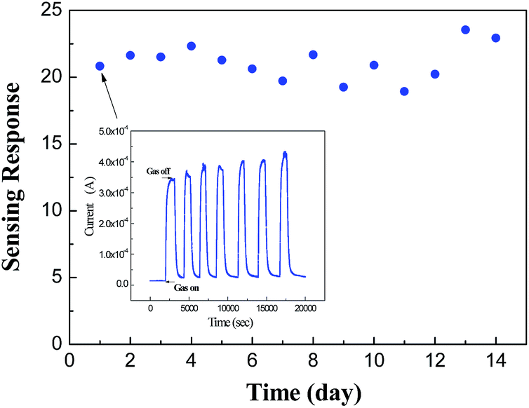
The gas-sensing stability of the CuO/V2O5 nanohybrids has been examined against 15 ppm H2S for a long period of time. In Fig. 10, the sensing response remains relatively stable with an average sensitivity of 21.1 during the continuous two-week measurement. Note that every response value is in fact an average of seven measurements (as shown in the inset for the first data point). This finding indicates that the CuO/V2O5 nanohybrids may be used in practical sensing applications for the selective detection of hazardous H2S gas, despite more work being required to elucidate the applicability.
 | ||
| Fig. 10 Gas-sensing stability of the CuO/V2O5 nanohybrids against 15 ppm H2S at 220 °C. | ||
Experimental section
A. Materials
CuO-functionalized V2O5 nanowires were prepared by a facile two-step route, involving hydrothermal and wet-deposition processes. In the hydrothermal process, crystalline V2O5 nanowires were synthesized from a solution mixture consisting of 0.285 g V2O5 powder in 9 ml de-ionized water, with dropwise addition of 1 ml hydrogen peroxide (35%) under vigorous agitation for 1 h. The solution was then placed in a Teflon-lined stainless-steel autoclave and kept at 180 °C for 24 h before being cooled down to room temperature naturally. The resultant V2O5 nanowires were washed repeatedly with de-ionized water, centrifuged and then dried at 80 °C. In the wet-deposition process, the as-prepared V2O5 nanowires were dispersed in a mixed solution consisting of 10 ml of ethanol and 0.06 g of Cu(NO3)2·3H2O. The suspension was then heated to 80 °C for the removal of ethanol. The powder was then placed in an alumina boat and fed into the centre of a three-zone horizontal quartz-tube furnace. The tube was first evacuated until the pressure inside reached 6 × 10⁻² torr, before the introduction of a gaseous mixture containing 85 sccm argon (standard cubic centimetres per min at STP) and 15 sccm oxygen. The temperature was then increased to 400 °C with a heating rate of 20 °C per min and held isothermally for 1 h with a continuous flow of the mixed gas during the entire heating process to prepare CuO nanoparticles decorated on V2O5 nanowires.B. Characterization
The morphology and crystalline structure of the V2O5 and CuO/V2O5 hybrid nanowires were examined by field-emission scanning electron microscopy (FE-SEM), X-ray diffractometry (XRD) with Cu Kα radiation (λ = 0.15405 nm) and transmission electron microscopy (TEM).C. Fabrication of the gas sensing devices
The gas sensors were fabricated by mixing the CuO/V2O5 hybrids or pristine V2O5 nanowires with methanol. The suspensions were then dispensed on alumina substrates with pre-configured, inter-digitated Ag electrodes. Analysis of the sensing properties was carried out in a self-assembled tubular furnace system along with a mass-flow controller, so that the concentration of various gases including air, H2S, CO and NO2 gases, could be precisely tuned. The electrical resistance was recorded by a volt-amperometric Keithley 2410 every 1 s over a wide range of gas concentrations (7 to 60 ppm) and working temperatures (100 to 400 °C) against target gases such as H2S, CO and NO2. For each test, the nanowire sensor was stabilized in air for 10 min before the target gas was introduced into the reaction chamber. The gas response (S) is defined as the ratio of the electrical resistance measured in fresh air (Ra) to the resistance measured in the presence of target gas (Rg). Either Ra/Rg or Rg/Ra was used for the determination of S, depending on the oxidising or reducing target gas used. The response time and recovery time are defined herein as the time it takes for the sensor to achieve 90% of its equilibrium level for the entire resistance change for adsorption and desorption of the target gas, respectively.Conclusion
Hybrid p-CuO/n-V2O5 nanowires were prepared via a facile chemical route and their gas-sensing properties were investigated. The formation of local p–n junctions at the nanometre scale CuO/V2O5 interface, together with the reversible sulfuric/oxidative reactivity when exposed to cyclic H2S gas/air at moderate temperatures, significantly enhanced the response and selectivity toward H2S gas sensing. The hybrid nanowires showed a rather indifferent response when CO and NO2 were used as the target gas. This unique selectivity toward H2S gas at precise ppm levels means that hybrid p-CuO/n-V2O5 nanowires are anticipated to be used in a stable and reliable sensing device suitable for practical alarm applications.Conflicts of interest
There are no conflicts to declare.Acknowledgements
We would like to dedicate this article to the late Professor Yung-Chiun Her who has inspired many friends and students alike with his boundless spirit and enthusiasm. His greatness is not merely reflected by the amount of wisdom he gave in and out of classroom, but even more by the way he always practiced what he preached. This study was supported financially by the Ministry of Science and Technology (Taiwan) under contract no. NSC101-2221-E005-033-MY3. Experimental assistance from students at the National Taichung First Senior High School is also gratefully acknowledged.References
- S. Ramasamy, S. Singh, P. Taniere, M. J. S. Langman and M. C. Eggo, Am. J. Physiol.: Gastrointest. Liver Physiol., 2006, 291, 288–296 CrossRef PubMed.
- V. E. Bochenkov and G. B. Sergeev, Sensitivity, selectivity, and stability of gas-sensitive metal-oxide nanostructures, in Metal Oxide Nanostructures and Their Applications, ed. A. Umar and Y.-B. Hahn, American Scientific Publishers, 2010, ch. 2, pp. 31–52 Search PubMed.
- H.-J. Kim and J.-H. Lee, Sens. Actuators, B, 2014, 192, 607–627 CrossRef CAS.
- S. M. Kanan, O. M. El-Kadri, I. A. Abu-Yousef and M. C. Kanan, Sensors, 2009, 9, 8158–8196 CrossRef CAS PubMed.
- J. Liu, X. Wang, Q. Peng and Y. Li, Adv. Mater., 2005, 17, 764–767 CrossRef CAS.
- J. Liu, X. Wang, Q. Peng and Y. Li, Sens. Actuators, B, 2006, 115, 481–487 CrossRef CAS.
- I. Raible, M. Burghard, U. Schlecht, A. Yasuda and T. Vossmeyer, Sens. Actuators, B, 2005, 106, 730–735 CrossRef CAS.
- A. D. Raj, P. S. Kumar, Q. Yang and D. Mangalaraj, Phys. E, 2012, 44, 1490–1494 CrossRef.
- A. D. Raj, T. Pazhanivel, P. S. Kumar, D. Mangalaraj, D. Nataraj and N. Ponpandian, Curr. Appl. Phys., 2010, 10, 531–537 CrossRef.
- V. Modafferi, G. Panzera, A. Donato, P. L. Antonucci, C. Cannilla, N. Donato, D. Spadaro and G. Neri, Sens. Actuators, B, 2012, 163, 61–68 CrossRef CAS.
- W. Yan, M. Hu, D. Wang and C. Li, Appl. Surf. Sci., 2015, 346, 216–222 CrossRef CAS.
- A. A. Mane, M. P. Suryawanshi, J. H. Kim and A. V. Moholkar, Appl. Surf. Sci., 2017, 403, 540–550 CrossRef CAS.
- A. A. Mane, M. P. Suryawanshi, J. H. Kim and A. V. Moholkar, J. Colloid Interface Sci., 2017, 495, 53–60 CrossRef CAS PubMed.
- X. Xue, L. Xing, Y. Chen, S. Shi, Y. Wang and T. Wang, J. Phys. Chem. C, 2008, 112, 12157–12160 CAS.
- F. Shao, M. W. G. Hoffmann, J. D. Prades, R. Zamani, J. Arbiol, J. R. Morante, E. Varechkina, M. Rumyantseva, A. Gaskov, I. Giebelhaus, T. Fischer, S. Mathur and F. Hernández-Ramírez, Sens. Actuators, B, 2013, 181, 130–135 CrossRef CAS.
- T.-S. Wang, Q.-S. Wang, C.-L. Zhu, Q.-Y. Ouyang, L.-H. Qi, C.-Y. Li, G. Xiao, P. Gao and Y.-J. Chen, Sens. Actuators, B, 2012, 171–172, 256–262 CrossRef CAS.
- S. Ahlers, G. Müller and T. Doll, Sens. Actuators, B, 2005, 107, 587–599 CrossRef CAS.
- R. Wang, S. Yang, R. Deng, W. Chen, Y. Liu, H. Zhang and G. S. Zakharova, RSC Adv., 2015, 5, 41050–41058 RSC.
- Y.-C. Her, B.-Y. Yeh and S.-L. Huang, ACS Appl. Mater. Interfaces, 2014, 6, 9150–9159 CAS.
- S.-W. Choi, A. Katoch, J.-H. Kim and S. S. Kim, J. Mater. Chem. C, 2014, 2, 8911–8917 RSC.
- B. G. Streetman and S. K. Banerjee, in Solid State Electronic Devices, Pearson Education Inc., New Jersey, 2005, pp. 144–238 Search PubMed.
- R. M. Abdel-Latif, Phys. B, 1998, 254, 273–276 CrossRef CAS.
- F. K. Butt, C. Cao, F. Idrees, M. Tahir, R. Hussain and A. Z. Alshemary, New J. Chem., 2015, 39, 5197–5202 RSC.
- H.-J. Zhai and L.-S. Wang, J. Chem. Phys., 2002, 117, 7882–7888 CrossRef CAS.
- V. Shrotriya, G. Li, Y. Yao, C. Chu and Y. Yang, Appl. Phys. Lett., 2006, 88, 073508 CrossRef.
Footnote |
| † Electronic supplementary information (ESI) available. See DOI: 10.1039/c7ra06657k |
| This journal is © The Royal Society of Chemistry 2017 |