
 Open Access Article
 This Open Access Article is licensed under a
 Creative Commons Attribution 3.0 Unported Licence
Ag-NPs doping enhanced resistive switching performance and induced changes in magnetic properties of NiFe2O4 thin films
Aize Hao,
Muhammad Ismail,
Shuai He ,
Ni Qin,
Wenhua Huang,
Jiang Wu and
Dinghua Bao*
,
Ni Qin,
Wenhua Huang,
Jiang Wu and
Dinghua Bao*
State Key Laboratory of Optoelectronic Materials and Technologies, School of Materials Science and Engineering, Sun Yat-Sen University, Guangzhou 510275, China. E-mail: stsbdh@mail.sysu.edu.cn
First published on 3rd October 2017
Abstract
Ag-NPs doped NiFe2O4 (NFO) thin films have been synthesized by the chemical solution deposition method. The effect of Ag-NPs incorporation on the resistive switching (RS) properties of NFO films with different doping concentrations in the range of 0 to 1.0% Ag was investigated. Results show that Ag-NPs doped NFO based memory devices perform resistive switching with much better uniformity and repeatability in switching cycles, and have excellent reliability at an appropriate Ag-NPs doping concentration (i.e. 0.5%) instead of very low and high doping concentrations (i.e. un-doped NFO film, 0.2% and 1.0% Ag). On the basis of analyses performed on current–voltage characteristics and their temperature dependence, it was found that the carrier transport occurred through the conducting filaments in the low resistance state with ohmic conduction, and in the high resistance state with Schottky emission. In addition, the temperature dependence of the resistance and magnetic behavior at HRS and LRS revealed that the physical origin of the RS mechanism, which involves the formation and rupture of the conducting paths, consists of oxygen vacancies and Ag atoms. Ag-NPs doping-induced changes in the saturation magnetization, associated with resistive switching, have been ascribed to variations in the oxygen vacancy concentration. The excellent endurance properties (>103 cycles), data retention (of >105 s at 298 and 358 K), and good cycle-to-cycle uniformity are observed in 0.5% Ag-NPs doped NFO-based memory devices.
1. Introduction
Resistive random access memory (RRAM) is considered as one of the most promising candidates for next generation non-volatile memories because of its simple capacitor-like metal-insulator-metal (MIM) structure, rapid switching speed, low power consumption, high storage density and non-volatile features.1–5 Due to resistance changes (high and low), RRAM is based on an electrical stimulus for receiving two logic states (“0” and “1”). Resistive switching (RS) has attracted significant attention in both academic and industrial communities due to its interesting physics and as well as future non-volatile memory (NVM) usage, which is compatible with complementary metal oxide semiconductor (CMOS) processing. For NVM, a variety of materials has been demonstrated for RS, such as binary transition metal oxides (NiO, ZrO2, and HfO2 etc.),6–8 multicomponent perovskite oxides (Pr0.7Ca0.3MnO3 and LaAlO3),9,10 as well as oxides of spinel ferrites.11–13 To date, there have been some scientific issues that are related to the RS mechanism and are also significant for NVM technology that have still not been resolved. To overcome such issues, diverse mechanisms have been proposed to explain observed RS behaviors, including the creation/break of conducting filaments, modification of the Schottky barrier height and electron trapping/detrapping.14In practical applications, some of the reliability issues should be resolved, which involve unstable switching behaviors, including large fluctuations in HRS and LRS, deterioration of endurance and retention time, and the controversial physical mechanism. Many efforts have been made to improve the performance of RS devices to satisfy the requirements of commercial applications, including impurity doping,15–18 using metal nanoparticles,19–27 bilayer structures,28,29 and interface control.30,31 Among these methods, introducing metal nanoparticles is the most extensive and popular method, which is highly effective for enhancing switching performance.23–26 Metal nanoparticles doping has been found to be helpful in enhancing the local electric field within the insulating layer, which consequently lowers the operating power consumption (electroforming, SET and RESET voltages) and improves RS characteristics. Recently, ZnO, NiO, BiFeO3, CoFe2O4, and Fe3O4 based films, undoped or doped with different valence nanoparticles (Ag, Mn, Co, etc.), have demonstrated adequate improvements in the RS characteristics.32–40 Wang et al. introduced Ag nanoclusters (Ag NCs) in ZnO-based devices, and explained the RS mechanism (which involves oxygen vacancy-based conducting filaments) due to the enhancement of the electric field around Ag NCs.23 Wang et al. also fabricated TaN/Al2O3:Ag:ZnO/ITO flexible RRAM devices embedded with Ag nanoparticles, which exhibited low power in-take, high speed, low set/reset voltages, high OFF/ON ratio, low resistance fluctuations, and superior retention performance.25 Gao et al. reported that reduction of the switching voltages, increased OFF/ON ratio up to 106, and improved stability of endurance were ascribed to the enhancement of the local electric field by embedded Ag NPs in Al2O3-based memory devices.26
Compared to other ferrite materials, NiFe2O4 (NFO) is among those important candidates in electronic and magnetic fields, which have been widely applied in resonators, phase shifters, tunable signal filters, and spintronics devices.41–44 In our previous study, the spinel structure-based NFO and ZnFe2O4 thin films exhibited outstanding RS performances.45,46 Currently, the research interest is focused towards whether an elegant approach would accomplish RS on inducing magnetic modulation, providing a unique opportunity to encode information in both RS and magnetic modulation to obtain four logic states. Recently, there has been significant interest in RRAM to realize the switching between insulating/conductive states along with ultra-high OFF/ON ratios and cyclic uniformity, whereas, the transition features of magnetic modulations accompanied by RS have been commonly ignored. It would be fundamentally informative if magnetic media had to be utilized in RRAM devices. Such facts have stimulated researchers to further investigate RS performance, its physical mechanism and magnetic properties in Ag-NPs doped NFO thin films.
In this study, Ag-NPs doped NFO based RRAM devices have been fabricated using different concentration of Ag nanoparticles. The present nonvolatile RS memory devices consisting of Ag-NPs doped NFO thin films not only demonstrate stable unipolar RS characteristics but also exhibit excellent uniformity in set/reset voltages and much longer retention times. The physical RS mechanism of Ag-doped NFO based devices, the temperature dependence of their resistance states and variations in the magnetic properties of these distinct resistance states have been explored in detail. In addition, a decrease in saturation magnetization has been noticed, which depends on the increase in Ag-NPs concentration in NFO films.
2. Experimental procedure
Ag-doped NFO thin films were prepared using the chemical solution deposition method.45,47 Precursor solutions of 0.2 M were synthesized using Ni(CH3COO)2·4H2O, Fe(NO3)3·9H2O, and AgNO3 as starting materials, and 2-methoxyethanol and acetic acid as co-solvent. The molar ratios of Ag to NFO were kept at 0![[thin space (1/6-em)]](https://www.rsc.org/images/entities/char_2009.gif) :1, 0.002:1, 0.005:1, 0.008:1 and 0.01:1, which were symbolized as NFO, NFO–Ag 0.2%, NFO–Ag 0.5%, NFO–Ag 0.8%, and NFO–Ag 1%, respectively. Precursor solutions were spin-coated onto Pt/Ti/SiO2/Si substrates at 3000 rpm for 30 s and baked at 300 °C for 5 min. The above spin coating and baking processes were repeated eight times and then, the deposited films were annealed at 750 °C for 1 h in air ambient. Finally, Pt top electrodes were deposited on the surface of the thin films using a metal shadow mask having a 300 μm diameter to complete the MIM memory devices.
:1, 0.002:1, 0.005:1, 0.008:1 and 0.01:1, which were symbolized as NFO, NFO–Ag 0.2%, NFO–Ag 0.5%, NFO–Ag 0.8%, and NFO–Ag 1%, respectively. Precursor solutions were spin-coated onto Pt/Ti/SiO2/Si substrates at 3000 rpm for 30 s and baked at 300 °C for 5 min. The above spin coating and baking processes were repeated eight times and then, the deposited films were annealed at 750 °C for 1 h in air ambient. Finally, Pt top electrodes were deposited on the surface of the thin films using a metal shadow mask having a 300 μm diameter to complete the MIM memory devices.
The crystal structure of the thin films was analyzed using an X-ray diffractometer (XRD, Rigaku D/MAX 2200 VPC) with Cu Kα radiation. The surface and cross-sectional morphologies of the thin films were investigated by field emission scanning electron microscopy (SEM, JSM-6330F). The defect or oxygen vacancy concentration in the film layer was examined by X-ray photoelectron spectroscopy (XPS, ESCLab250). The film microstructure was inspected in detail using high resolution transmission electron microscope (HRTEM, JEOL JEM 2010HR). The resistive switching characteristics, i.e. repetitive cycling of the current–voltage (I–V) measurements were performed using the Keithley 236 sourcemeter in DC sweep mode under air ambient at room temperature. Temperature dependent resistances for HRS and LRS in the range of 150 to 300 K were also measured. The magnetic hysteresis loops were measured at room temperature using a superconducting quantum interference device (SQUID) magnetometer (Quantum Design). The maximum applied magnetic field was 2 tesla and thin film samples were placed parallel to the applied magnetic field.
3. Results and discussion
Fig. 1 shows XRD patterns of Ag (0%, 0.2%, 0.5%, 0.8%, and 1%) doped NFO thin films deposited on Pt/Ti/SiO2/Si substrates. It can be observed that except for a few XRD reflections related to the substrates, all of the observed peaks correspond to the reflections of the cubic spinel lattice of NFO (JCPDS card no. 54-0964), indicating single phase spinel structure without the presence of impurity phases.45 No Ag-related diffraction peaks were clearly observed.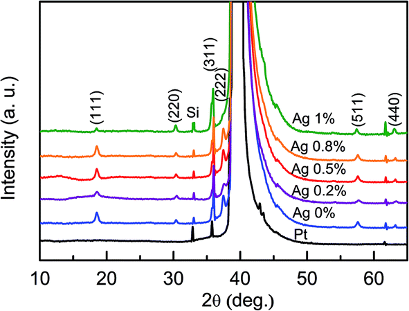 | ||
| Fig. 1 X-ray diffraction patterns of NFO films with different Ag-NPs doping concentrations on Pt/Ti/SiO2/Si substrates annealed at 750 °C in ambient air. | ||
Surface morphology images of NFO thin films with different Ag-NPs doping concentrations deposited on Pt/Ti/SiO2/Si substrates and annealed at 750 °C in air ambient are shown in Fig. 2(a–e). These micrographs indicate that thin films are smooth with almost uniformly distributed nanocrystalline particles. It is notable that crystallite size first decreases and then increases with increasing AgNPs concentration. The larger crystallites typically possess relatively better crystallinity and good stability in RS characteristics. The cross-sectional SEM image of the heterostructure is shown in Fig. 2(f), demonstrating that the Ag-NPs (1%) doped NFO film has a thickness of approximately 370 nm.
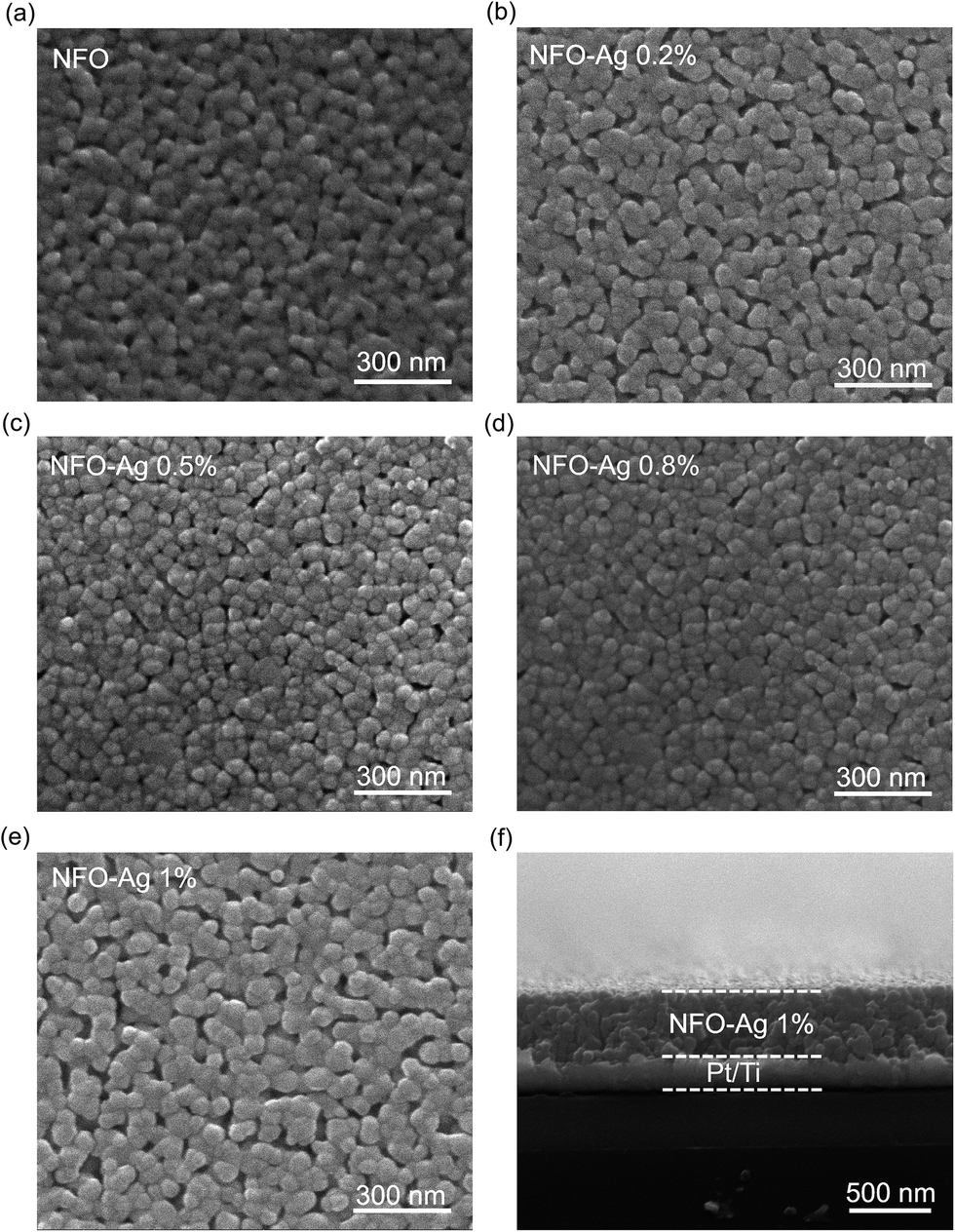 | ||
| Fig. 2 SEM surface morphology images of NFO films with different Ag-NPs doping concentrations on Pt/Ti/SiO2/Si substrates annealed at 750 °C in ambient air: (a) NFO; (b) NFO–Ag 0.2%; (c) NFO–Ag 0.5%; (d) NFO–Ag 0.8%; (e) NFO–Ag 1%. (f) Cross-sectional SEM micrograph of NFO–Ag 1% thin films on Pt/Ti/SiO2/Si substrates. | ||
XPS analysis was carried out to examine the surface chemical compositions and the valence states of Ni, Fe, O, and Ag species involved in the device by inspecting the spectral line shape and signal intensities associated with the core-level electrons. XPS spectra of Ni 2p, Fe 2p, O 1s, and Ag 3d of Ag-NPs (0.5%) doped NFO-based thin film device are shown in Fig. 3(a–d). As illustrated in Fig. 3(a), Ni 2p3/2 peaks centered at 854.8 eV and 855.9 eV correspond to Ni2+ (Oh) and Ni2+ (Td), respectively; the 2p1/2 binding energies at 872.3 eV and 874.2 eV are associated with Ni2+ (Oh) and Ni2+ (Td), respectively. The two satellite peaks are located at 861.6 eV and 879.2 eV. Similarly, the Fe 2p spectrum can be resolved into three peaks: the first one is ascribed to Fe2+, while the remaining two are caused by two lattice sites of Fe3+ ions as indicated in Fig. 3(b). The binding energies associated with Fe2+, Fe3+ (Oh), and Fe3+ (Td) of Fe 2p3/2 states are 709.7 eV, 711.1 eV and 712.7 eV, respectively, and those of Fe 2p1/2 states exist at 722.9 eV, 724.0 eV, and 725.7 eV. Fig. 3(c) shows the high resolution XPS O 1s spectrum. The lower fitting binding energy peak located at 529.8 eV corresponds to the lattice oxygens, while the higher binding energy peak centered at 531.6 eV is attributed to the non-lattice or defective oxygens present in the thin films. The Ag 3d5/2 and Ag 3d3/2 binding energies, located at 367.7 eV and 374.0 eV, indicate the oxidation states of silver and metallic silver, respectively (Fig. 3(d)).44 XPS results indicate the presence of oxygen vacancies in the active oxide (NFO) layer, which are modified by the increasing concentration of Ag-NPs in the NFO thin films. In the present study, various chemical states observed for Ni, Fe, O and Ag elements in the Ag-NPs (0.5%) doped NFO-based thin films are in good agreement with their values given in literature.43,44,47
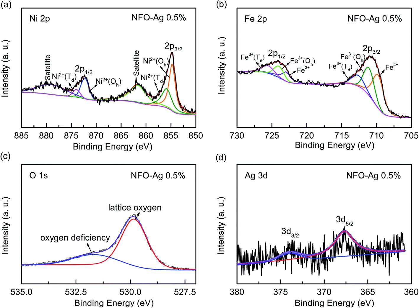 | ||
| Fig. 3 XPS spectra of NFO–Ag 0.5% thin film: (a) Ni 2p region, (b) Fe 2p region, (c) O 1s region, and (d) Ag 3d region. | ||
To further investigate the distribution and chemical states of Ag-NPs doped NFO-based thin films, detailed analysis was conducted through TEM characterizations. For this purpose, Ag-NPs (1%) doped NFO-based thin films were peeled off from the substrates and dispersed in ethanol. These films were then examined through TEM. Fig. 4(a) shows a typical TEM image, which was further magnified to select a few areas for further analyses; three such selected areas (marked as A, B and C) are presented in Fig. 4(b). The area A contains particles with diameters of around 50 nm, while areas B and C consist of particles with diameters of around 20 nm. The crystal structures of Ag-NPs (1%) doped NFO-based thin films were studied by selected area electron diffraction (SAED) patterns. The SAED of these areas are marked by the red circles in Fig. 4(c). The diffraction spots in the SAED patterns have been successfully indexed, while the phases of NFO and Ag were further confirmed by comparing XRD JCPDS cards (no. 54-0964 and no. 04-0783) (Table 1). As demonstrated by Fig. 4(d), HRTEM images of these selected areas depict interplanar distances of 0.48 nm, 0.27 nm, and 0.24 nm, corresponding well to the lattice spacing of the NFO (111), Ag2O (111), and Ag (111) planes, respectively. These observations together with changes in morphology and color of these phases suggest that both metallic and oxidized Ag phases coexist in the NFO thin films; analogous situations have been noticed by other researchers.47,48
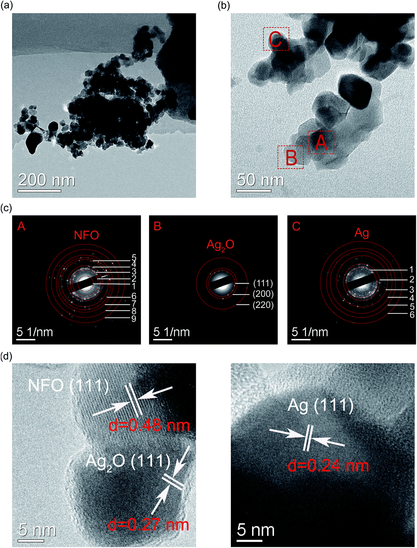 | ||
| Fig. 4 (a) TEM image of NFO–Ag 1% film; (b) a magnified TEM image illustrating three selected areas (A, B and C) for further analysis. (c) The selected area electron diffraction (SAED) patterns for regions A, B and C. (d) The corresponding HRTEM images of regions A, B and C. | ||
| Results of SAED (A area) | XRD results of NFOa | Results of SAED (C area) | XRD results of Agb | ||||
|---|---|---|---|---|---|---|---|
| Circle | dhkl (nm) | Facet | dhkl (nm) | Circle | dhkl (nm) | Facet | dhkl (nm) |
| a JCPDS card no. 54-0964.b JCPDS card no. 04-0783. | |||||||
| 1 | 0.4863 | (111) | 0.48106 | 1 | 0.2385 | (111) | 0.23590 |
| 2 | 0.2915 | (220) | 0.29465 | 2 | 0.2082 | (200) | 0.20440 |
| 3 | 0.2534 | (311) | 0.25129 | 3 | 0.1464 | (220) | 0.14450 |
| 4 | 0.2071 | (400) | 0.20840 | 4 | 0.1285 | (311) | 0.12310 |
| 5 | 0.1458 | (440) | 0.14738 | 5 | 0.1042 | (400) | 0.10215 |
| 6 | 0.1303 | (620) | 0.13186 | 6 | 0.0922 | (331) | 0.09375 |
| 7 | 0.1216 | (622) | 0.12569 | ||||
| 8 | 0.1145 | (642) | 0.11142 | ||||
| 9 | 0.0979 | (660) | 0.9827 | ||||
The activation phenomenon for switching the device from the OFF state (HRS) to the ON state (LRS), occurring for the first time at relatively high fields, is generally called “electroforming”; it is usually essential for initiating the memory devices. In this regard, bias voltages in the range from 0 to +25 V using current compliance (CC) of 10 mA were applied to all the devices. The initiation of resistive switching in all the pristine devices was achieved through a positive bias voltage when voltages (Vform) reached at least +10 V, and such a high bias voltage can be associated with the requirement of inducing the conductive paths in the pristine devices. Fig. 5(a) clearly illustrates that forming voltages (Vform) decrease by increasing the Ag-NPs doping concentration. After completing the forming process, when the positively biased voltage was varied in the range of 0 to 4 V, the resistances of all the devices suddenly returned to the value of the OFF-state resistance (HRS), called the “reset process”, as shown in Fig. 5(b–f), which implies the rupture of conducting filaments. With further increase in the positively biased voltage applied to the Pt top electrode (TE), all the devices resistances abruptly changed from the OFF-state (HRS) value to the ON-state (LRS); this transition occurred when the positive bias voltages were in the range of 2 to 4 V, with a CC of 5–10 mA, and was designated the “set process” (Fig. 5(b–f)). These resistance changes were expected, due to the formation of conducting filaments in Ag-doped NFO-based RRAM devices. It is noted that the switching characteristics of Pt/NFO–Ag 0.5%/Pt and Pt/NFO–Ag 1%/Pt devices are much more stable than Pt/NFO/Pt and Pt/NFO–Ag 0.2%/Pt devices. The reset and set processes have been observed for the same voltage polarity applied to all the devices, which suggest that the memory devices show stable and repeatable unipolar RS behavior.
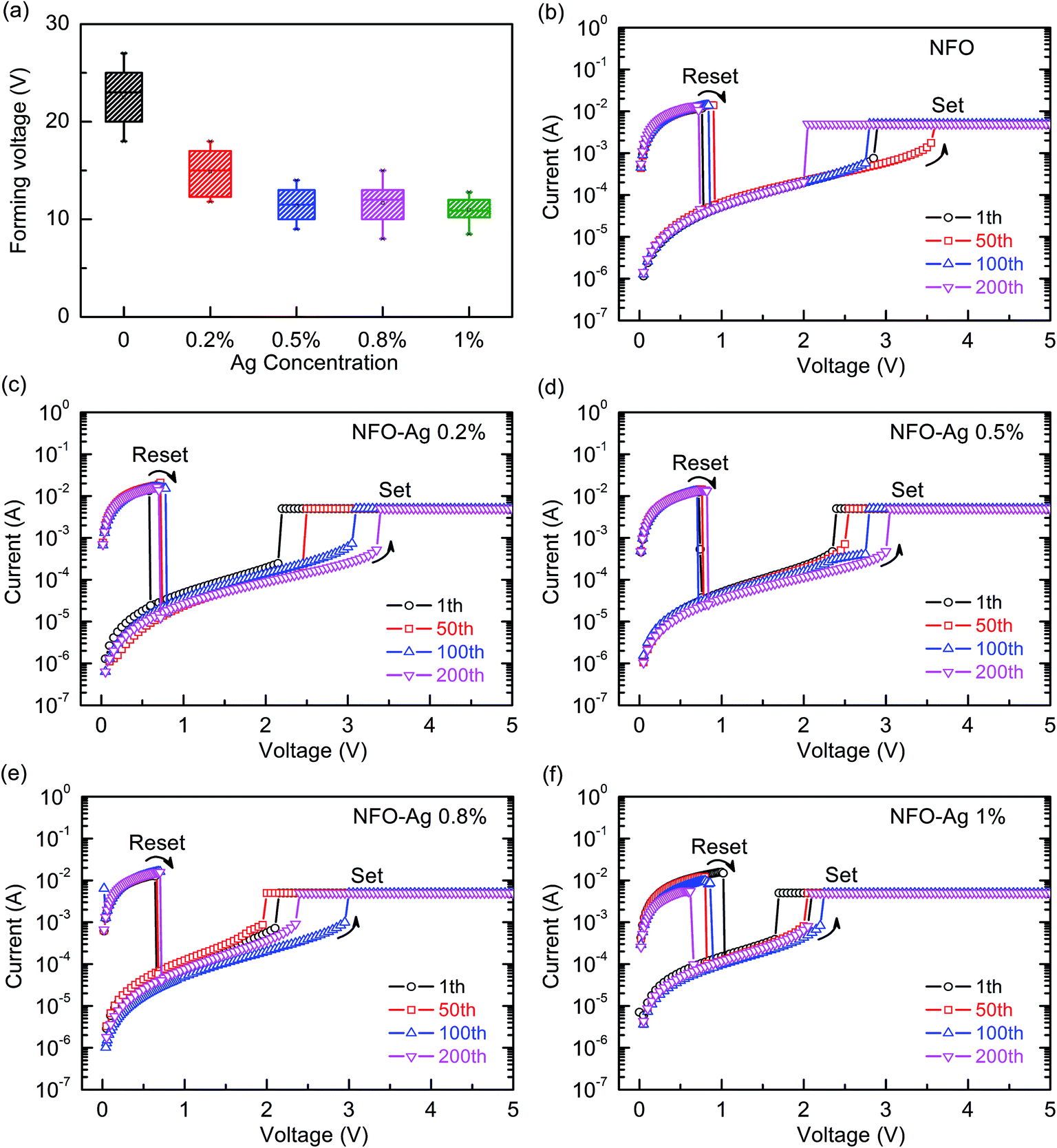 | ||
| Fig. 5 (a) Variations of electroforming voltages with changing Ag-NPs doping concentrations. Typical current–voltage curves recorded during repetitive switching cycles after the electroforming process in (b) Pt/NFO/Pt, (c) Pt/NFO–Ag 0.2%/Pt, (d) Pt/NFO–Ag 0.5%/Pt, (e) Pt/NFO–Ag 0.8%/Pt, and (f) Pt/NFO–Ag 1%/Pt memory devices. | ||
Superb consistency is desirable for the manufacture of NVM devices. To meet the necessities of device reliability, the results of the statistical distribution of SET (VSET) and RESET (VRESET) voltages and their dependence on Ag-NPs concentration are shown in Fig. 6. Regarding this, the operational voltages were measured on each device for the first 100 trials. For the pure NFO based devices, the statistical distribution graph (Fig. 6(a)) depicts that SET and RESET voltages indicate much wider variations from +0.6 to +1.2 V and from +1.5 to +4.0 V, respectively. However, this variation (illustrated in Fig. 6(b)), as a statistical distribution for 0.2% Ag-NPs doped devices, ranges from +0.5 to +1.0 V (VSET) and from +1.4 to +4.0 V (VRESET). However, optimum variations in VSET and VRESET distributions were obtained for 0.5% Ag-NPs doped devices, which range from +0.6 to +0.9 V and from +2.2 to +3.2 V, respectively. It was further noticed that for Ag-NPs doping with 0.5%, the variations of VSET and VRESET were minimum as compared to all other devices in Fig. 6(c). When the Ag-NPs doping concentration was higher than 0.5%, both VSET and VRESET showed an increased variation (Fig. 6(d)), which ranged from +0.7 to +1.2 V and from +1.7 to +2.6 V, respectively. Interestingly, appropriate Ag-NPs doping concentrations can remarkably improve RS stability and uniformity. Similar improvement has also been demonstrated in Pt/ZnO/Al devices with doping of Ag nanoclusters,23 Al2O3-based devices with Ag nanoparticles doping,24,25 and TaN/Al2O3/ZnO/ITO flexible devices with embedded Ag nanoparticles.26
 | ||
| Fig. 6 Statistical distribution of the SET and RESET voltages of NFO thin films with various Ag-NPs doping concentrations: (a) undoped, (b) 0.2% Ag, (c) 0.5% Ag, and (d) 1.0% Ag. | ||
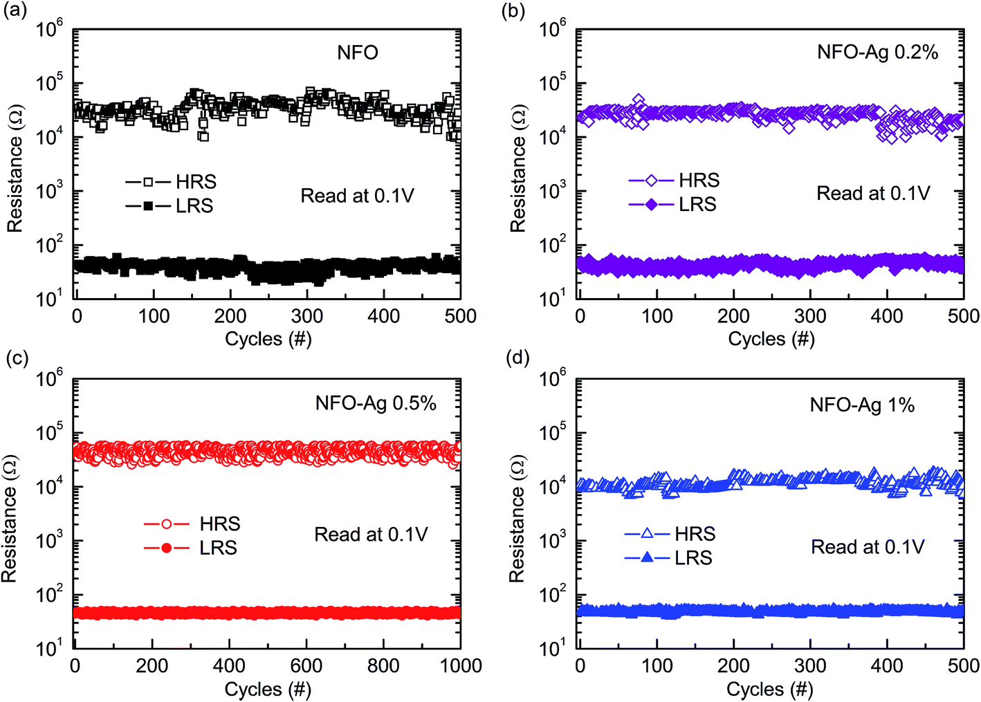
To understand the potential of Ag-NPs doped NFO based devices, the reliability of the impulsive switching endurance was considered in both LRS and HRS as shown in Fig. 7. These DC endurance tests were performed at a read voltage of 0.1 V. During the repetitive switching cycles, fluctuations in the resistances of both LRS and HRS were observed, particularly in HRS, for both undoped and 0.2% Ag-doped devices (Fig. 7(a and b)). This type of behavior might occur due to the generation of less oxygen vacancies21 in pure NFO and Ag-NPs (0.2%)-doped NFO based devices. The resistance values are quite stable, particularly in Ag-NPs (0.5% and 1%)-doped NFO based devices (Fig. 7(c and d)). The particle size of Ag-NPs (≤20 nm) is smaller than that of the NFO crystallites (≥50 nm). As AgNO3 was added to the precursor solution, which was spin coated on the Pt bottom electrode, it is expected that Ag-NPs might be randomly distributed throughout the NFO layer, which could also diffuse into the NFO layer along grain boundaries by the application of biasing fields to rearrange themselves. These Ag-NPs were expected to create oxygen vacancies because of their better oxygen extracting abilities and could form silver oxide (Ag2O) as verified by the SAED and HRTEM results illustrated in Fig. 4(c and d).48 Such degradation/fluctuation can be avoided by balancing the generation and annihilation of oxygen vacancies in the filaments by increasing the concentration of Ag-NPs.21 On increasing Ag-NPs concentration to 0.5%, the endurance performance remains stable up to 1000 DC switching cycles without any significant degradation. Thus, by providing optimum Ag-NPs concentration, oxygen vacancies and/or Ag cations might adjust themselves in such a way that the device shows stable endurance characteristics for a large number of DC switching cycles. However, on further increasing Ag-NPs concentrations up to 1%, the device again demonstrates the set/reset instability in the resistive window (Fig. 7(d)). Because of an appropriate Ag-NPs concentration, most of the defects could be removed and oxygen vacancies might be relatively filled; also, due to the existence of silver oxide (Ag2O), as observed through SAED data (Fig. 4), there remains a lesser possibility for electrons to be trapped and hence, degradation in the RS properties is expected.22
 | ||
| Fig. 7 Endurance test of the LRS and HRS of Ag-doped NFO thin films with various doping concentrations: (a) undoped, (b) 0.2% Ag, (c) 0.5% Ag, and (d) 1% Ag. | ||
An improvement in the resistance states of NFO-based RRAM devices was found to be consistent with the narrowing distribution of switching voltages with increasing Ag-NPs content (Fig. 7). The switching transitions involve the connection and disconnection of conducting filaments inside the Ag-doped NFO layer. During the RESET process, some parts of the conducing filaments are ruptured. Consequently, the state and shape of the residual conducting filaments determine the magnitudes of VSET and VRESET in the subsequent SET process. The very stable HRS and LRS in 0.5% Ag-NPs doped devices imply that conducting filaments are ruptured at similar positions/locations during each RESET process, which therefore results in a quite constant VSET value to reconnect the ruptured filaments. It has already been reported that the conducting filaments are preferably formed along or near the grain boundaries of the polycrystalline films,45 and therefore the location and shape of the conducting filaments can be affected by both the crystallinity and availability of the charge carriers in the dielectric film.
Fig. 8(a) shows the retention characteristics of Pt/NFO–Ag 0.5%/Pt devices measured at room temperature. The Ag-NPs doped NFO based devices exhibited constant resistance values for 105 s, indicating highly durable HRS and LRS. For estimating the retention properties for a further prolonged period or at high temperatures, Ag-NPs doped NFO based devices were exposed to a temperature of 85 °C for more than 105 s, demonstrating the excellent nondestructive readout capability; the corresponding resistance values in HRS and LRS were monitored (Fig. 8(b)). However, the HRS was noted to decrease by approximately one order of magnitude in resistance, corresponding to the semiconducting-like transport phenomenon of the oxide films.
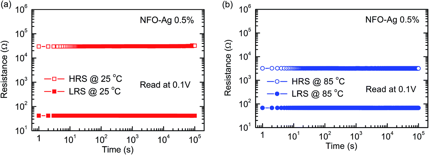 | ||
| Fig. 8 Retention capability in HRS and LRS of Pt/NFO–Ag 0.5%/Pt devices (a) at 25 °C and (b) at 85 °C. | ||
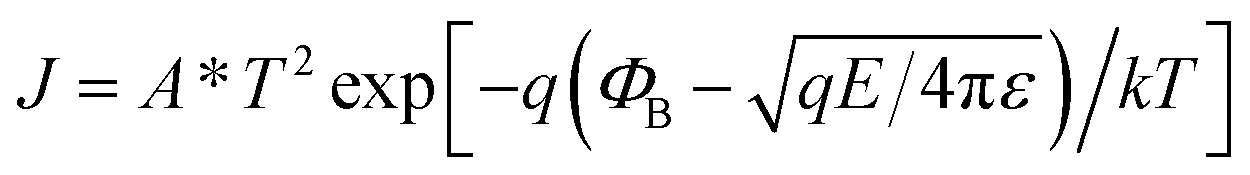
To uncover the underlying RS mechanism, the I–V data can be redrawn in accordance with the requirements of the existing theories of charge carrier transport. In this regard, Fig. 9(a) displays the double logarithmic plots for both LRS and HRS to investigate the conduction mechanisms of resistive switching in Pt/NFO–Ag 0.5%/Pt devices. In the LRS, the conduction mechanism is ohmic as indicated by the unit slope (0.97) in Fig. 9(a). This figure also clarifies HRS operation obeying Ohm's law in the low field region (up to 1.0 V) with a slope of ∼1.09. This means that thermally generated free carriers are greater in number than the injected carriers, which is why current depends upon the applied bias and resistance of the dielectric film. However, in the high filed region of HRS, we need to further investigate the conduction mechanism that is dominantly operative because the slope value in this region (bias voltage > 1.0 V, Fig. 9(a)) is greater than 2 (∼3.73). This means that in this high electric field area, charge transport does not follow the space-charge-limited conduction. In this high field region, either the interface-limited Schottky emission (SE) or bulk-limited Poole–Frenkel (PF) emission can play the dominant role to conduct charge in the Ag-NPs doped NFO memory devices. These two mechanisms can be described by the following equations:
 | (1) |
 | (2) |
 | ||
| Fig. 9 (a) The double-log scale I–V curves for resistive switching of Pt/NFO–Ag 0.5%/Pt devices. (b) Typical ln(I) versus V1/2 plot in the higher voltage region of the HRS. (c) The ln(I/T2) versus 1/T plot for HRS of Pt/NFO–Ag 0.5%/Pt devices studied at 1.4 V, 1.6 V and 1.8 V. (d) Arrhenius type plots of ln(I) versus 1/T in HRS. (e) Temperature dependence of resistances in the HRS and LRS of Pt/NFO–Ag 0.5%/Pt devices observed at bias voltage of 0.1 V; (f) the resistance temperature R(T) coefficient α at LRS with different Ag-doping concentrations of Pt/NFO/Pt memory devices. | ||
To analyze I–V data in accordance with SE and PF conduction, plots of ln(I) (SE plot) and ln(I/V) (PF plot) as a function of the square root of applied voltage (√V) were drawn in the high field region (bias voltage > 1.0 V, Fig. 9(a)); the plots are displayed in Fig. 9(b). The ln(I)–√V curve represents a good linear fit, following the Schottky emission mechanism in comparison to the Poole–Frenkel conduction fit (inset plot) (Fig. 9(b)).45,49 Based on electrical conduction mechanism analyses, it can be concluded that ohmic and SE conductions are the respectively dominating transport mechanisms in the low and high field regions of Ag-NPs (0.5%) doped NFO-based devices.
To further investigate the mechanism of temperature dependence of the Pt/NFO–Ag 0.5%/Pt devices, I–V characteristics in the HRS were examined and analyzed as a function of temperature. The temperature dependent I–V data measured at bias voltages of 1.4, 1.6, and 1.8 V were then plotted as ln(I/T2) versus 1/T in HRS of Ag-NPs doped films (as presented in Fig. 9(c)). The plots are depicted as straight lines, which reveal that the conduction mechanism follows Schottky emission.49 Fig. 9(d) illustrates Arrhenius type plots of ln(I) versus 1/T curves recorded at 1.4, 1.6, and 1.8 V. These plots are linear with negative slopes in the studied temperature region, suggesting that the transport mechanism obeys the following Arrhenius type expression: I(T) ∝ exp(−Ea/kBT), where Ea is the thermal activation energy and kB is the Boltzmann constant. The thermal activation energy for charge conduction was obtained to be about 0.27 eV, illustrating that HRS of these Ag-NPs doped films complies with the semiconducting behavior.
In addition, dependence of electrical resistance on the temperature is an effective way to reveal the RS conduction mechanism. The constitution of conductive filaments could be verified by the temperature dependence of resistances of the Ag-NPs doped NFO based devices at both LRS and HRS as depicted in Fig. 9(e). The current in LRS decreases slightly with increasing temperature as resistance in the LRS increases with a rise in temperature. Such type of conduction agrees well with metallic conducting behavior, and could be attributed to the formation of conducting filaments in the Ag-NPs doped NFO based films. In contrast, the magnitude of current in HRS increases almost linearly with the increase in temperature, which indicates an insulating or semiconducting like behavior of the oxide film. Temperature dependent I–V characteristics demonstrate that LRS increases and HRS decreases in resistance with increase in temperature in the range of 150 to 300 K. These results indicate the metallic- and semiconducting-like characteristics at these two states, supporting the creation of oxygen vacancies and Ag metal based conducting filaments. However, the formation of Ag-oxide (Ag2O), as observed/confirmed through the HRTEM and SAED results (Fig. 4(c and d)), might act as hindrance sites to the flow of current and hence, LRS might rise in resistance.
Further evidence for the presence of metallic Ag filaments can be obtained by applying the concept of the temperature coefficient of resistance. In this regard, the temperature dependent resistance in LRS of Ag-NPs doped NFO based devices was fitted in accordance with the well-known equation, R(T) = Ro[1 + α(T − To)], to determine the temperature coefficient of resistance (α). The temperature coefficients of resistance in the LRS of NFO based devices as a function of Ag-NPs doping concentration are plotted and shown in Fig. 9(f). It is noted that the coefficient “α” increases non-linearly with increasing Ag-NPs doping concentration. The coefficients “α” for un-doped NFO based devices (6.5 × 10⁻⁴ K−1) and Ag-NPs (0.2%) doped NFO-based devices (7.8 × 10⁻⁴ K−1) were found to be very similar to those obtained for oxygen vacancy-based conductive filaments, i.e. 5.6 × 10⁻⁴ K−1 or 6.0 × 10⁻⁴ K−1,23,45 indicating that the conductive filaments are mainly composed of oxygen vacancies. However, the magnitudes of coefficients “α” obtained for NFO devices doped with higher concentrations of Ag-NPs were found to be much larger than those for oxygen vacancy-based conductive filaments (5.6 × 10⁻⁴ K−1).45 However, their values are lower than, but closer to those of Ag–metal based conductive filaments (i.e. 4.2 × 10⁻³ K−1),50,51 suggesting that the conductive filaments in Pt/NFO–Ag/Pt devices with high doping concentration of Ag-NPs are composed of not only oxygen vacancies but also Ag atoms.
In addition to this, some researchers have proposed the role of Ag atoms in forming metallic conducting filaments. Gao et al. have demonstrated that CFs are formed by both oxygen vacancies and Ag atoms in Ti/Al2O3/AgNPs/Al2O3/p-Si memory devices.26 Chung et al. reported that conducting filaments are composed of Ag atoms in Ag/TaOx/Pt devices working at 300 K.52 Shi et al. suggested that Ag particles act as seeds for conducting filaments, leading to depressed randomness and reduced diameter of the conducting paths.53 In the light of these facts, it may be proposed that Ag atoms can also contribute in the formation of conducting filaments.
The magnetic properties associated with RS are interesting and meaningful in spinel ferrite oxides. The magnetic hysteresis loops of NFO–Ag thin films obtained at 300 K are shown in Fig. 10(a); the signals appeared due to Pt/Ti/SiO2/Si substrates have been subtracted. It is noted that all of the devices have demonstrated ferromagnetic behavior with varying Ag-NPs doping concentration in NFO films. Moreover, the saturation magnetization is noticed to be decreasing from a value of 175.1 emu cm−3 to 135.4 emu cm−3 with increasing concentration of Ag-NPs in the devices. It is further indicated by Fig. 10(b) that at the same concentration of Ag-NPs (0.5%) NFO-based thin films, saturation magnetization depicts remarkable variations with the change of resistance states, e.g., a decrease in saturation magnetization occurred in the order of virgin device, to the device in HRS, to that in LRS. The changes in magnetic properties can be explained on the basis of the fact that Ag-doping poses variations in the electronic properties of NFO thin films, which consequently reduce the spin polarization of Fe 3d states; this reduction weakens the magnetic coupling of Fe spins. In addition, the interface-dipole induced electron transfer might cause a reduction in the spin moment of Fe ions,54 and, Ag-NPs might deter the lining up for the polarization of magnetic domains with applied magnetic field.54 To understand the role that oxygen vacancies and Ag-NPs doping play in the unipolar RS mechanism, the investigations on the magnetic properties at different resistance states of the device are required. Such investigations (illustrated in Fig. 10(b)) involve the M–H hysteresis loops of Ag-NPs (0.5%) doped NFO-based devices in their “fresh state” as well as in HRS and LRS at 300 K. One can observe various hysteresis loops observed in different states (LRS and HRS), indicating that RS is accompanied by changes in magnetism of Ag-NPs doped NFO based films. The saturation magnetization relationship was found to be MS (Fresh) > MS (HRS) > MS (LRS) in Ag-NPs (0.5%) doped NFO-based devices. The variations in saturation magnetization with different resistance states could be attributed to Ag-NPs doping-induced variation in oxygen vacancies concentration and this could also involve contributions from changes in valence states of Fe3+ and Fe2+ ions at octahedral sites.45 Our earlier study also indicated that oxygen vacancies generation resulted in changes in magnetization at different resistance states in NFO films.45 Moreover, Chen et al. have also reported the variations in oxygen vacancies modulated magnetism in Pt/Co:ZnO/Pt devices.32 Ren et al. proposed that the resistive switching effects and magnetism could be tuned and linked with the movement of oxygen vacancies in Ag/Ti/Fe3O4/Pt devices using an applied electric field.35
 | ||
| Fig. 10 (a) M–H loops of NFO thin films with different Ag-NPs doping concentrations on Pt/Ti/SiO2/Si substrates at 300 K; (b) M–H loops of Pt/NFO–Ag 0.5%/Pt devices under various resistance states at 300 K. | ||
On the basis of the above analysis related to conductive filaments, a physical mechanism of resistive switching could be explained in Ag-NPs doped NFO based devices using the model of formation/rupture of conducting filaments by considering the thermal effects of oxygen vacancies and electrochemical metallization effects.26,45,46,52,53,55,56 Fig. 11(a) is schematic plot of the mechanism involving the formation/rupture of conducting filaments in pure NFO-based devices. The oxygen vacancies can be easily generated to form conducting filaments by the application of the electric field to the top electrode, which also assists the creation of conductive filaments during the set process. During the reset process, the conducting filaments are ruptured by the Joule heating effect, due to the large flow of current in the LRS, accompanied by a decrease of oxygen vacancies. It is noteworthy that the formation/rupture of conductive filaments is a highly random process, which leads to serious switching instability in the memory devices. Likewise, in un-doped NFO based memory devices, the dominant conducting paths in Ag-NPs (0.2%) doped NFO-based devices are also mainly composed of oxygen vacancies. Therefore, the formation/rupture of conducting filaments is also related to oxygen vacancies and Joule heating effects. However, for NFO-based devices with higher Ag-NPs doping concentration, the dominant conductive paths not only involve oxygen vacancies but also Ag atoms based on our obtained temperature coefficient of resistance. Therefore, on the basis of joint contributions of oxygen vacancies and metallic Ag, a model is being proposed to explore the physical mechanism of RS in Ag-NPs doped NFO-based devices. As illustrated in Fig. 11(b), during the set process Ag-NPs might provide movable Ag+ ions and some of these Ag+ ions drift toward the Pt bottom electrode, thereby reducing the number of Ag atoms involved to develop part of the conducting filaments. Moreover, the local electric field (LEF) is expected to be enhanced around Ag atoms, due to applied bias voltage causing the non-uniform distribution of the electric field, which could consequently assist the generation of conical-shaped conducting filaments; analogous behavior has also been reported in the literature.23,24,26 As the reduction process to Ag+ ions becomes difficult, oxygen vacancies might connect part of the conducting filaments containing Ag atoms along the direction of LEF to form simple and/or radial shaped local conducting paths. Such conducting paths could be dissolved in switching locations by the Joule heating effect during the reset process. As discussed above, Ag-NPs might contribute to forming the conducting channels; the RS might become localized in crossing segments between Ag atoms and oxygen vacancies along the direction of LEF. This results in the reduction of randomness in the formation/rupture of the conductive paths and good uniformity in the RS process and stability of HRS and LRS. From the above discussion, it can be deduced that the conducting paths for RS could be localized by appropriate Ag-NPs doping concentrations in spinel ferrite based memory devices.
 | ||
| Fig. 11 Schematic diagrams of formation/rupture in conducting filaments for (a) the Pt/NFO/Pt device, and (b) Pt/NFO–Ag (0.5%, 0.8%, 1%)/Pt devices. | ||
4. Conclusions
Ag-NPs doped NFO thin films were synthesized by the spin-coating technique, and the effect of Ag-NPs concentration on RS characteristics of the memory devices was investigated. The observed improvement in the stability and uniformity of switching parameters is attributed to the reduction in the randomness of conducting filaments' formation/rupture by appropriate Ag-NPs doping concentration. The conduction mechanism in the high and low resistance states is dominated by Schottky emission and ohmic conduction. On the basis of analyses performed on current–voltage characteristics and temperature dependence of resistances in HRS and LRS, it is concluded that the resistive switching mechanism could be due to the combined effect of oxygen vacancies and the Ag electrochemical metallization effect. The saturation magnetization was observed to decrease with increase in Ag-NPs concentration in NFO based memory devices. The changes in saturation magnetization associated with resistive switching are ascribed to the variations in oxygen vacancy concentration by Ag-NPs doping during the RS process. The notable saturation magnetization variations at HRS and LRS, remarkably suitable ON/OFF ratio, good endurance (>1000 cycles) and highly stable retention (at 298 K and 358 K) were observed for an appropriate concentration of Ag-NPs (i.e. 0.5%) in doped NFO based devices. The present results are indicative of the fact that doping of Ag-NPs in spinel ferrite thin films is a feasible approach to improve their resistance, switching behavior and magnetic properties, and provides a new avenue for designing multifunctional electromagnetic devices.Conflicts of interest
The authors declare no competing financial interest.Acknowledgements
The authors gratefully acknowledge financial support from Natural Science Foundation of Guangdong Province, China (No. 2015A030311019) and Natural Science Foundation of China (No. 51372281).References
- A. Sawa, Mater. Today, 2008, 11, 28–36 CrossRef CAS
.
- R. Waser, R. Dittmann, G. Staikov and K. Szot, Adv. Mater., 2009, 21, 2632–2663 CrossRef CAS
- R. Waser and M. Aono, Nat. Mater., 2007, 6, 833–840 CrossRef CAS PubMed
- K. M. Kim, D. S. Jeong and C. S. Hwang, Nanotechnology, 2011, 22, 254002 CrossRef PubMed
- T.-C. Chang, K.-C. Chang, T.-M. Tsai, T.-J. Chu and S. M. Sze, Mater. Today, 2016, 19, 254–264 CrossRef CAS
- S. Seo, M. J. Lee, D. H. Seo, E. J. Jeoung, D. S. Suh, Y. S. Joung, I. K. Yoo, I. R. Hwang, S. H. Kim, I. S. Byun, J. S. Kim, J. S. Choi and B. H. Park, Appl. Phys. Lett., 2004, 85, 5655–5657 CrossRef CAS
- Q. Liu, J. Sun, H. B. Lv, S. B. Long, K. B. Yin, N. Wan, Y. T. Li, L. T. Sun and M. Liu, Adv. Mater., 2012, 24, 1844–1849 CrossRef CAS PubMed
- S. M. Yu, H. Y. Chen, B. Gao, J. F. Kang and H. S. Philip Wong, ACS Nano, 2013, 7, 2320–2325 CrossRef CAS PubMed
- A. Sawa, T. Fujii, M. Kawasaki and Y. Tokura, Appl. Phys. Lett., 2004, 85, 4073–4075 CrossRef CAS
- X. L. Jiang, Y. G. Zhao, X. Zhang, M. H. Zhu, H. Y. Zhang, D. S. Shang and J. R. Sun, Appl. Phys. Lett., 2013, 102, 233501 CrossRef
- Z. W. Li, M. X. Zhou, W. F. Ding, H. Zhou, B. Chen, J. G. Wan, J. M. Liu and G. H. Wang, Appl. Phys. Lett., 2012, 100, 262903 CrossRef
- V. Thakare, G. Xing, H. Peng, A. Rana, O. Game, P. Anil Kumar, A. Banpurkar, Y. Kolekar, K. Ghosh, T. Wu, D. D. Sarma and S. B. Ogale, Appl. Phys. Lett., 2012, 100, 172412 CrossRef
- W. Hu, L. L. Zou, R. Q. Chen, W. Xie, X. M. Chen, N. Qin, S. W. Li, G. W. Yang and D. H. Bao, Appl. Phys. Lett., 2014, 104, 143502 CrossRef
- F. Pan, S. Gao, C. Chen, C. Song and F. Zeng, Mater. Sci. Eng., R, 2014, 83, 1–59 CrossRef
- W. Lee, J. Park, S. Kim, J. Woo, J. Shin, D. Lee, E. Cha and H. Hwang, Appl. Phys. Lett., 2012, 100, 142106 CrossRef
- H. W. Zhang, B. Gao, B. Sun, G. P. Chen, L. Zeng, L. F. Liu, X. Y. Liu, J. Lu, R. Q. Han, J. F. Kang and B. Yu, Appl. Phys. Lett., 2010, 96, 123502 CrossRef
- H. W. Zhang, L. F. Liu, B. Gao, Y. J. Qiu, X. Y. Liu, J. Lu, R. Q. Han, J. F. Kang and B. Yu, Appl. Phys. Lett., 2011, 98, 042105 CrossRef
- M. S. Lee, S. Choi, C. H. An and H. Kim, Appl. Phys. Lett., 2012, 100, 143504 CrossRef
- W.-Y. Chang, K.-J. Cheng, J.-M. Tsai, H.-J. Chen, F. Chen, M.-J. Tsai and T.-B. Wu, Appl. Phys. Lett., 2009, 95, 042104 CrossRef
- Q. Liu, S. B. Long, H. B. Lv, W. Wang, J. B. Niu, Z. L. Huo, J. N. Chen and M. Liu, ACS Nano, 2010, 4, 6162–6168 CrossRef CAS PubMed
- J. H. Yoon, J. H. Han, J. S. Jung, W. Jeon, G. H. Kim, S. J. Song, J. Y. Seok, K. J. Yoon, M. H. Lee and C. S. Hwang, Adv. Mater., 2013, 25, 1987–1992 CrossRef CAS PubMed
- P. Cui, S. Seo, J. Lee, L. Wang, E. Lee, M. Min and H. Lee, ACS Nano, 2011, 5, 6826–6833 CrossRef CAS PubMed
- Z. Q. Wang, H. Y. Xu, L. Zhang, X. H. Li, J. G. Ma, X. T. Zhang and Y. C. Liu, Nanoscale, 2013, 5, 4490–4494 RSC
- S.-C. Qin, R.-X. Dong and X.-L. Yan, Appl. Phys. A, 2015, 118, 605–612 CrossRef CAS
- D.-T. Wang, Y.-W. Dai, J. Xu, L. Chen, Q.-Q. Sun, P. Zhou, P.-F. Wang, S.-J. Ding and D. W. Zhang, IEEE Electron Device Lett., 2016, 37, 878–881 CrossRef CAS
- L. Gao, Y. Li, Q. Li, Z. Song and F. Ma, Nanotechnology, 2017, 28, 215201 CrossRef PubMed
- Z. Xu, M. Gao, L. Yu, L. Lu, X. Xu and Y. Jiang, ACS Appl. Mater. Interfaces, 2014, 6, 17823–17830 CAS
- J. Lee, E.-M. Bourim, W. Lee, J. Park, M. Jo, S. Jung, J. Shin and H. Hwang, Appl. Phys. Lett., 2010, 97, 172105 CrossRef
- M. J. Lee, C. B. Lee, D. Lee, S. R. Lee, M. Chang, J. H. Hur, Y. B. Kim, C. J. Kim, D. H. Seo, S. Seo, U. I. Chung, I. K. Yoo and K. Kim, Nat. Mater., 2011, 10, 625–630 CrossRef CAS PubMed
- D. C. Kim, M. J. Lee, S. E. Ahn, S. Seo, J. C. Park, I. K. Yoo, I. G. Baek, H. J. Kim, E. K. Yim, J. E. Lee, S. O. Park, H. S. Kim, U. I. Chung, J. T. Moon and B. I. Ryu, Appl. Phys. Lett., 2006, 88, 232106 CrossRef
- M. Ismail, E. Ahmed, A. M. Rana, F. Hussain, I. Talib, M. Y. Nadeem, D. Panda and N. A. Shah, ACS Appl. Mater. Interfaces, 2016, 8, 6127–6136 CAS
- G. Chen, C. Song, C. Chen, S. Gao, F. Zeng and F. Pan, Adv. Mater., 2012, 24, 3515–3520 CrossRef CAS PubMed
- D. Li, W. Zheng, D. Zheng, J. Gong, L. Wang, C. Jin, P. Li and H. Bai, ACS Appl. Mater. Interfaces, 2016, 8, 3977–3984 CAS
- M. Zhao, Y. D. Zhu, Q. W. Wang, M. Wei, X. L. Liu, F. Zhang, C. Hu, T. T. Zhang, D. Qiu, M. Y. Li and R. Xiong, Appl. Phys. Lett., 2016, 109, 013504 CrossRef
- S. X. Ren, X. T. Song, G. W. Sun, X. Zhao, H. F. Yang and W. Chen, J. Mater. Chem. C, 2013, 1, 7879–7882 RSC
- X. X. Chen, X. J. Zhu, W. Xiao, G. Liu, Y. P. Feng, J. Ding and R. W. Li, ACS Nano, 2015, 9, 4210–4218 CrossRef CAS PubMed
- Q. W. Wang, Y. D. Zhu, X. L. Liu, M. Zhao, M. C. Wei, F. Zhang, Y. Zhang, B. L. Sun and M. Y. Li, Appl. Phys. Lett., 2015, 107, 063502 CrossRef
- K. Zhang, Y. L. Cao, Y. W. Fang, Q. Li, J. Zhang, C. G. Duan, S. S. Yan, Y. F. Tian, R. Huang, R. K. Zheng, S. S. Kang, Y. X. Chen, G. L. Liu and L. M. Mei, Nanoscale, 2015, 7, 6334–6339 RSC
- X. Li, J. Jia, Y. Li, Y. Bai, J. Li, Y. Shi, L. Wang and X. Xu, Sci. Rep., 2016, 6, 31934 CrossRef CAS PubMed
- D. Zhao, S. Qiao, Y. Luo, A. Chen, P. Zhang, P. Zheng, Z. Sun, M. Guo, F. K. Chiang, J. Wu, J. Luo, J. Li, S. Kokado, Y. Wang and Y. Zhao, ACS Appl. Mater. Interfaces, 2017, 9, 10835–10846 CAS
- U. Lüders, M. Bibes, J.-F. Bobo, M. Cantoni, R. Bertacco and J. Fontcuberta, Phys. Rev. B: Condens. Matter Mater. Phys., 2005, 71, 134419 CrossRef
- U. Lüders, A. Barthélémy, M. Bibes, K. Bouzehouane, S. Fusil, E. Jacquet, J. P. Contour, J. F. Bobo, J. Fontcuberta and A. Fert, Adv. Mater., 2006, 18, 1733–1736 CrossRef
- S. Anjum, G. H. Jaffari, A. K. Rumaiz, M. S. Rafique and S. I. Shah, J. Phys. D: Appl. Phys., 2010, 43, 265001 CrossRef
- G. H. Jaffari, A. K. Rumaiz, J. C. Woicik and S. I. Shah, J. Appl. Phys., 2012, 111, 93906 CrossRef
- W. Hu, N. Qin, G. H. Wu, Y. T. Lin, S. W. Li and D. H. Bao, J. Am. Chem. Soc., 2012, 134, 14658–14661 CrossRef CAS PubMed
- W. Hu, X. M. Chen, G. H. Wu, Y. T. Lin, N. Qin and D. H. Bao, Appl. Phys. Lett., 2012, 101, 063501 CrossRef
- L. Su, N. Qin, T. L. Sa and D. H. Bao, Opt. Express, 2013, 21, 29425–29434 CrossRef PubMed
- Y. Yang, P. Gao, S. Gaba, T. Chang, X. Pan and W. Lu, Nat. Commun., 2012, 3, 732 CrossRef PubMed
- W. Hu, L. L. Zou, X. M. Chen, N. Qin, S. W. Li and D. H. Bao, ACS Appl. Mater. Interfaces, 2014, 6, 5012–5017 CAS
- A. Bid, A. Bora and A. K. Raychaudhuri, Phys. Rev. B: Condens. Matter Mater. Phys., 2006, 74, 035426–035433 CrossRef
- K.-Y. Shin, Y. Kim, F. V. Antolinez, J. S. Ha, S.-S. Lee and J. H. Park, Adv. Electron. Mater., 2016, 2, 1600233 CrossRef
- Y.-L. Chung, W.-H. Cheng, J.-S. Jeng, W.-C. Chen, S.-A. Jhan and J.-S. Chen, J. Appl. Phys., 2014, 116, 164502 CrossRef
- L. Shi, D. S. Shang, Y. S. Chen, J. Wang, J. R. Sun and B. G. Shen, J. Phys. D: Appl. Phys., 2011, 44, 455305 CrossRef
- S. H. Liu, H. M. Tsai, C. W. Pao, J. W. Chiou, D. C. Ling, W. F. Pong, M. H. Tsai, H. J. Lin, L. Y. Jang, J. F. Lee, J. H. Hsu, W. J. Wang and C. J. Hsu, Appl. Phys. Lett., 2006, 89, 092112 CrossRef
- Y. C. Yang, F. Pan, Q. Liu, M. Liu and F. Zeng, Nano Lett., 2009, 9, 1636–1643 CrossRef CAS PubMed
- J. Y. Son, C. H. Kim, J. H. Cho, Y. H. Shin and H. M. Jang, ACS Nano, 2010, 4, 3288–3292 CrossRef CAS PubMed
| This journal is © The Royal Society of Chemistry 2017 |