
 Open Access Article
 This Open Access Article is licensed under a
 Creative Commons Attribution 3.0 Unported Licence
Regular conjugated D–A copolymer containing two benzotriazole and benzothiadiazole acceptors and dithienosilole donor units for photovoltaic application
M. L. Keshtov*a,
S. A. Kuklina,
A. R. Khokhlova,
I. O. Konstantinova,
N. V. Nekrasova b,
Zhi-yuan Xiec and
Ganesh D. Sharma*d
b,
Zhi-yuan Xiec and
Ganesh D. Sharma*d
aInstitute of Organoelement Compounds of the Russian Academy of Sciences, Vavilova St., 28, 119991 Moscow, Russian Federation. E-mail: keshtov@ineos.ac.ru
bInstitute of Physical Chemistry and Electrochemistry of the Russian Academy of Sciences, Leninsky Prospect, 31, Moscow, 119071, Russian Federation
cState Key Laboratory of Polymer Physics and Chemistry, Changchun Institute of Applied Chemistry, Chinese Academy of Sciences, Changchun 130022, P. R. China
dDepartment of Physics, The LNM Institute for Information Technology, Jamdoli, Jaipur, India. E-mail: gdsharma273@gmail.com
First published on 20th October 2017
Abstract
Herein, we report the synthesis and characterization of a regular D1–A1–D1–A2–D2–A2 conjugated copolymer with an optical bandgap of 1.53 eV, denoted as PTBTfBTzSi consisting of two acceptors i.e. benzothiadizole (A1) flanked with two thiophene donors (D1) and fluorinated benzotriazole (A2) with one more donor dithienosilole (D2) and investigated its optical and electrochemical properties. The highest occupied molecular orbital and lowest unoccupied molecular orbital energy levels of PTBTfBTzSi are estimated from cyclic voltammetry measurements and are −5.38 eV and −3.67 eV, respectively. We have used this copolymer as a donor along with a PC71BM as acceptor for the fabrication of solution processed BHJ polymer solar cells (PSCs). The PSC based on the optimized PTBTfBTzSi:PC71BM active layer (weight ratio 1![[thin space (1/6-em)]](https://www.rsc.org/images/entities/char_2009.gif) :1.5 and 3 v% 1,8-diiodooctance (DIO)) as a solvent additive in chloroform, showed overall PCE of 8.91% (short circuit current of 14.36 mA cm−2, open circuit voltage of 0.94 V and fill factor of 0.66) which is higher than that of PSC based on a chloroform cast active layer (4.95% with a short circuit current of 9.53 mA cm−2, open circuit voltage of 0.98 V and fill factor of 0.53). The higher PCE is attributed to the balanced charge transport, elevated light harvesting efficiency and more favorable nanoscale morphology and enhanced crystallinity of the active layer processed with the solvent additive. Moreover, the energy loss in our polymer solar cell is 0.59 eV which is one of the lowest values among the most of the efficient polymer solar cells reported so far based on a fullerene based acceptor, to the best of our knowledge.
:1.5 and 3 v% 1,8-diiodooctance (DIO)) as a solvent additive in chloroform, showed overall PCE of 8.91% (short circuit current of 14.36 mA cm−2, open circuit voltage of 0.94 V and fill factor of 0.66) which is higher than that of PSC based on a chloroform cast active layer (4.95% with a short circuit current of 9.53 mA cm−2, open circuit voltage of 0.98 V and fill factor of 0.53). The higher PCE is attributed to the balanced charge transport, elevated light harvesting efficiency and more favorable nanoscale morphology and enhanced crystallinity of the active layer processed with the solvent additive. Moreover, the energy loss in our polymer solar cell is 0.59 eV which is one of the lowest values among the most of the efficient polymer solar cells reported so far based on a fullerene based acceptor, to the best of our knowledge.
1. Introduction
Polymer solar cells (PSCs) based on bulk heterojunction (BHJ) active layers that consist of a mixer of conjugated polymers (donor) and fullerene derivatives, have been considered promising technology for converting light energy into electrical energy, due to their many advantages such as low cost of fabrication from a solution processing method, light weight, mechanical flexibility, and roll to roll production.1 During the last few years, many efficient molecular design strategies have been adopted to tailor the optical and electrochemical properties of organic semiconducting materials used for organic solar cells such as donor–acceptor (D–A) structure modification, side chain engineering, and functional group modification,2 leading to the devices with a power conversion efficiency of 11% for fullerene based acceptors3 and in the range of 11–13% for non-fullerene small molecule acceptors.4 In D–A copolymers, the band gap is controlled by the intramolecular charge transfer (ICT) between the donor (D) and acceptor (A) units. In general, by employing D and A units with different strengths in the D–A backbone of the copolymer, the bandgap can be significantly reduced. Moreover, introducing a third monomer either donor or acceptor in the D–A backbone, i.e. A1–D–A2–D or A–D1–A–D2–A, the optical and electrochemical properties can be easily tuned leading to the improvement in the power conversion efficiency (PCE) of the resulted PSCs.5 It was reported that the regioregular D–A copolymers showed higher charge carrier mobility and crystallinity than its random counterpart due to the improved π–π stacking interactions which are beneficial for achieving the high PCE of PSCs.6In comparison to low bandgap copolymers, development the wide bandgap D–A copolymers is another alternative to enhance the device performance by the optimization of open circuit voltage (Voc) and charge extraction from the active layer by electrodes.7 Therefore, it is necessary to design new wide bandgap copolymers with excellent photovoltaic properties in addition to low bandgap copolymers. Copolymers with wide bandgap can be designed in the form of D–A structure by incorporation of moderate electron donating and electron withdrawing units.8 In this line, Sun et al. has designed a wide bandgap copolymer with bandgap of 1.85 eV which showed high PCE of 9.7% when used as donor in BHJ-PSCs.8d Among the various electron acceptor units reported for the designing of wide bandgap D–A polymers, benzotriazole (BTz) unit has attracted much interest, since the lone pair electrons at the 2-position nitrogen atom reduces the electron accepting ability relative to benzothiadiazole (BT).8a,9 The central nitrogen can be functionalized with an alkyl chain not only increase the solubility but also separates from the conjugated backbone to reduce the steric hindrance, thereby enhancing the effective interchain π-conjugation and packing leading to higher charge carrier mobility. Recently, Lan et al. has designed a wide bandgap D–A copolymer using BTz as acceptor unit in the backbone and used it as donor component for BHJ active layer for PSCs and achieved PCE of 8.63%.10
Recently, it is has been demonstrated that incorporation of fluorine atom in the electron acceptor unit of the polymer backbone and is regarded one of the most promising approach for enhancing the photovoltaic performance of the PSCs.11 The high electron affinity and small size of fluorine atom can effectively modulate the band gap of copolymer by lowering both HOMO and LUMO energy levels and also minimize the undesirable steric hindrance of conjugated polymers. In recent past, large number of electron donating and accepting units has been developed for PSCs and the copolymers based on D–A–D–A–D–A structure are more efficient than that of their D–A counterparts. Moreover, the bandgap as well as energy levels of former copolymers can be fine-tuned or optimized with the combination of one weak donor with one strong donor, or combination of one weak acceptor and one strong acceptor units. Recently, Wang et al. have designed ternary conjugated copolymers using indenothiophene (bridged by a thiophene) and benzodithiophene as the weak and the strong donor units, respectively along with fluorinated benzothiadiazole as the strong acceptor moiety and achieved PCE of 9.08% for BHJ-PSC using PC71BM as acceptor.12
In this study we report the synthesis of a new D1–A1–D1–A2–D2–A2 conjugated copolymer denoted as PTBTfBTzSi that contains two acceptors i.e. BT (A1) flanked with two thiophene (D1) donors and fluorinated benzotriazole (fBTz) (A2) and one donor dithienosilole (DTS) (D2) and investigated its optical and electrochemical properties. We have used this copolymer as donor along PC71BM as electron acceptor for the fabrication of solution processed BHJ PSCs. After the optimization of active layer (adjusting donor to acceptor weight ratios and concentration of 1,8-diiodooctane (DIO) solvent additive (3 v%) in host chloroform (CF), the resultant PSC showed overall PCE of 8.91% with an energy loss of 0.59 eV which is lowest among the PSC based on fullerene acceptor to the best of our knowledge).
2. Experimental
2.1. Materials
Pd(PPh3)4 was purchased from Alfa Aesar Chemical Co. and used as received without further purification. Toluene was dried over molecular sieves and distilled prior to use. All other chemicals and solvents (analytical-grade) were used without further purification.2.2. Characterization
1H NMR spectra of the copolymer in chloroform solution at 298 K temperature was recorded using a Bruker AV-400 spectrometer. Chemical shifts were reported in ppm with tetramethylsilane (TMS) as the internal reference. Molecular weight and polydispersity index (PDI) of the copolymer were determined by gel permeation chromatography (GPC) analysis with polystyrene used as reference. Thermo gravimetric analysis (TGA) in nitrogen atmosphere was conducted using Perkin Elmer TGA-7 at heating rate of 10 °C min−1. The UV-vis absorption spectra of copolymer in solution and thin film were recorded with Hitachi U-3010 UV-vis spectrophotometer. Cyclic voltammetry was recorded with a computer controlled ZahnerIM6e electrochemical work station at a scan rate of 50 mV s−1. The copolymer film was coated on carbon electrode (1.0 cm2) and used as the working electrode. A platinum wire and Ag/Ag (0.1 M) were used as the counter and reference electrodes, respectively. An anhydrous and argon-saturated solution of 0.1 M tetra-butylammonium-hexafluorophosphate (Bu4NPF6) in acetonitrile solution was used as electrolyte. The morphology of the copolymer/PC71BM blend films were investigated by a SPI 3800N atomic force microscope (AFM) in contacting mode with a 3 mm scanner.2.3. Synthesis
Monomers 4,7-bis(5-(trimethylstannyl)thiophene-2-yl)benzo[c][1,2,5]thiadiazole M1 (ref. 13) and 2,6-bis(7-bromo-6-fluoro-2-hexyl-2H-benzotriazol-4-yl)-4,4-bis(2-ethylhexyl)-4H-silolo-[3,2-b:4,5-b′]dithiophene M2 (ref. 14) have been synthesized as reported in our earlier communications. The synthetic route for the synthesis of PTBTfBTzSi was shown in Scheme 1.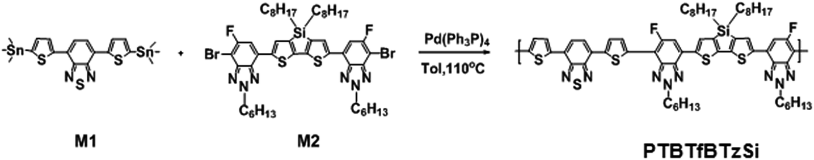 | ||
| Scheme 1 Synthetic route for PTBTfBTzSi. | ||
2.4. Synthesis of poly[(4,7-bis(thiophen-2-yl)benzo[c][1,2,5]thiadiazole)-alt-(2,6-bis(6-fluoro-2-hexyl-2H-benzotriazol-4-yl)-4,4-bis(2-ethylhexyl)-4H-silolo[3,2-b:4,5-b′]dithiophene) (PTBTfBTzSi)
Compound (M1) (0.4234 g, 0.5 mmol) and compound (M2) (0.5076 g, 0.5 mmol) were dissolved in dry (18 mL) toluene and solution was flushed with argon for 20 min. After that Pd(Ph3P)4 (27 mg, 0.023 mmol) was added into the flask. The flask was purged three times with successive vacuum and argon filling cycles and then kept in the oil bath and heated up to 110 °C. The mixture was carefully stirred for 48 h at above temperature under an argon atmosphere. The reaction mixture was cooled to room temperature and then poured slowly into methanol (300 mL). The resulting precipitate was filtered through a Soxhlet thimble and then subjected to Soxhlet extractions with methanol, hexane and chloroform, sequentially. Finally the solid form of copolymer was recovered from the chloroform fraction by rotary evaporation. The dark green solid was dried under vacuum at 60 °C overnight (0.398 g, yield: 69%). GPC (CHCl3): Mn = 10.4 kDa; PDI = 1.94. 1H-NMR (400 MHz, CDCl3, δ ppm): 8.40–7.31 (br, 10H, Ar), 4.83–4.79 (br, 4H, N–CH2), 2.29–0.69 (br, 56H, Alk). 19F-NMR (400 MHz, CDCl3, δ ppm): −110.65. Anal. calcd for (C62H70F2N8S5Si1)n, %: C, 64.55; H, 6.12; F, 3.29; N, 9.71; S, 13.90; Si, 2.43. Found, %: C, 64.00; H, 6.04; F, 3.11; N, 9.29; S, 13.61; Si, 2.17.2.5. Device fabrication and characterization
Indium tin oxide (ITO) coated glass substrates were cleaned in ultrasonicated bath containing detergent, deionized water acetone and iso-propanol sequentially and then dried in vacuum oven at 40 °C for overnight. A solution of polyethylenedioxy-thiophene:polystyrenesulfonate (PEDOT:PSS, Clevios Al4083) was spin coated onto the pre-cleaned ITO substrate at 3500 rpm for 30 min and subsequently annealed at 120 °C for 10 min in air environment. The mixer of electron donor PTBTfBTzSi and electron acceptor PC71BM in different weight ratios were dissolved in chloroform solution with a total concentration of 14 mg mL−1 and then spin coated on top of the PEDOT:PSS film for 30 s at 1500 rpm and at ambient conditions and dried for 2 h. For solvent additive (SA), 3 v% of DIO was mixed into the host CF solvent. A methanol solution of poly[9,9-bis(3′-(N,N-dimethylamino)propyl)2,7-fluorene)-alt-2,7-(9,9-dioctylfluorene] (PFN) with a concentration of 1.5 mg mL−1 was then spin-coated on top of the active layer at 3000 rpm for 30 s. Finally the aluminium (Al) (90 nm) was deposited on top of the active layers by means thermal evaporation under a pressure of 10−5 Torr. The active area is about 16 mm2 which is defined as the vertical overlap of ITO and Al electrodes. We have fabricated hole-only (ITO/PEDOT:PSS/active layer/Au) and electron only (ITO/Al/active layer/Al) devices to measure the hole and electron mobility respectively. A computer controlled Keithley's Source meter was used to measure the current–voltage (J–V) characteristics of the PSCs in ambient conditions and the illumination AM1.5 G (100 mW cm−2) provided by a solar simulator. The incident photon-to-current efficiency (IPCE) of the devices was measured by illuminating the devices using a light source and the monochromator and the resulting current was measured using a Keithley electrometer under short-circuit conditions.3. Results and discussion
3.1. Synthesis and characterization of poly[(4,7-bis(thiophen-2-yl)benzo[c][1,2,5]thiadiazole)-alt-(2,6-bis(6-fluoro-2-hexyl-2H-benzotriazol-4-yl)-4,4-bis(2-ethylhexyl)-4H-silolo[3,2-b:4,5-b′]dithiophene) (PTBTfBTzSi)
The synthetic route of the copolymer PTBTfBTzSi is shown in Scheme 1. The PTBTfBTzSi was synthesized by palladium-catalyzed Stille-coupling reaction of monomers M1 and M2 and carefully purified by sequential Soxhlet extractions with methanol, hexane, and CHCl3. Then CHCl3 fraction was concentrated under vacuum evaporation and then precipitated into methanol and finally collected by filtration. The chemical structure of the copolymer was verified by 1H-NMR and 19F-NMR (Fig. 1). The characteristic broad signals at 8.4–7.3 ppm can be assigned to the resonance of proton. The phenyl ring and thiophene ring, –CH2– protons linking to nitrogen are at 4.81 ppm, and the signal observed at 2.257–0.69 ppm corresponds to the protons of the long alkyl chain. The absence of the characteristic singlet peak at 0.4 ppm in the 1H-NMR spectrum reveals that no trimethyltin end groups are present in PTBTfBTzSi. These results along with elemental analysis indicate that the polymerization reaction was successfully completed. The number-average molecular weight (Mn) and PDI of PTBTfBTzSi are 10.4 and 1.94, respectively. The obtained copolymer is soluble in common organic solvents such as chloroform, toluene, and chlorobenzene.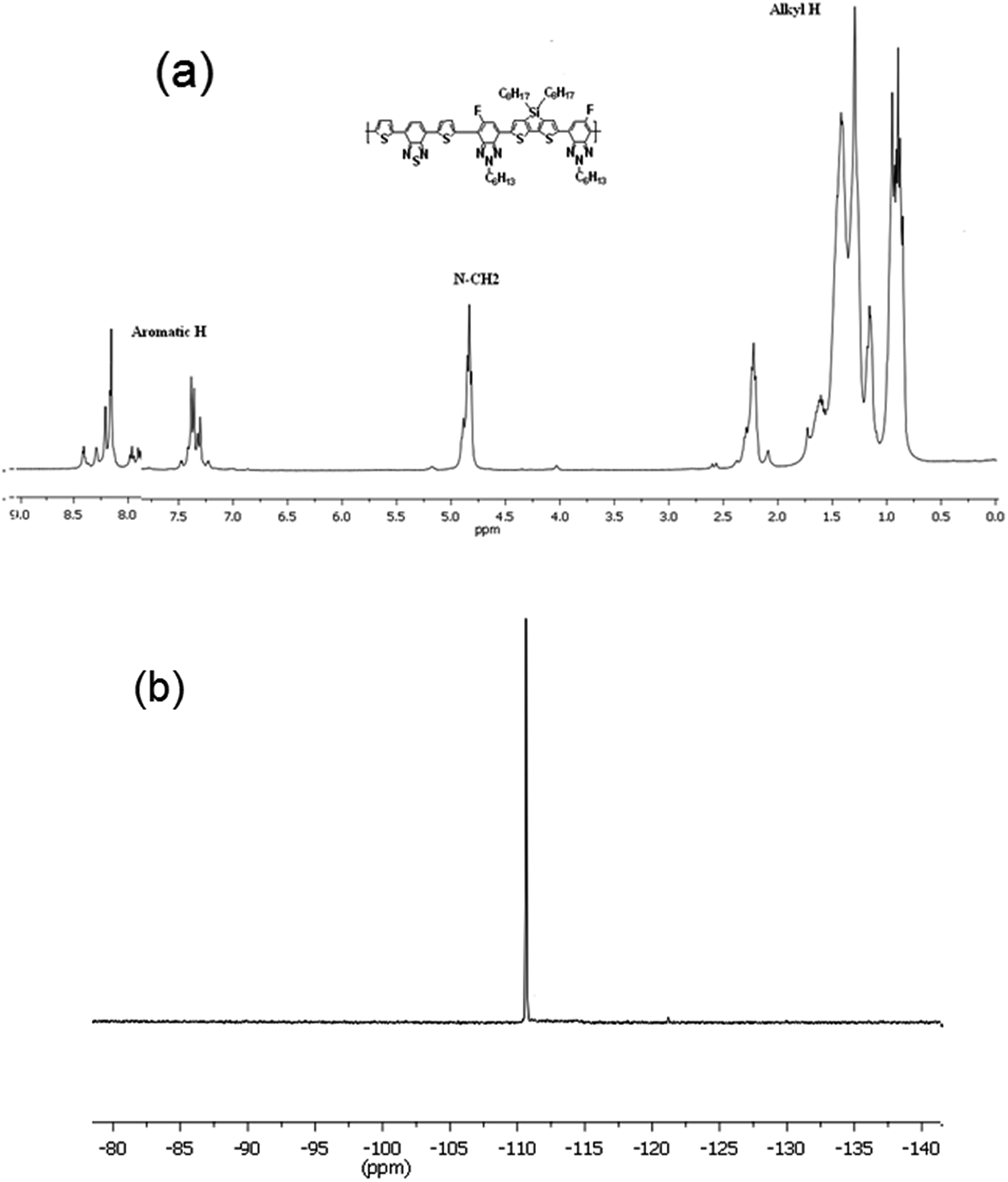 | ||
| Fig. 1 (a) 1H-NMR and (b) 19F-NMR spectra of the polymer PTBTfBTzSi in CDCI3. | ||
The thermal property of the copolymer was investigated by thermogravimetric analysis (TGA) under flow of nitrogen at a heating rate of 10 °C min−1 and shown in Fig. 2. As shown in Fig. 2, TGA indicated that the PTBTfBTzSi exhibited good thermal stability with 5% weight loss temperature (Td) of 393 °C. Therefore, the thermal property of PTBTfBTzSi is adequate for its application in photovoltaic solar cells and other optoelectronic devices.
 | ||
| Fig. 2 TGA curves of the polymer PTBTfBTzSi with a heating rate of 10 °C min−1. | ||
3.2. Optical and electrochemical properties
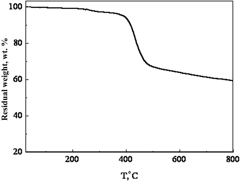
Fig. 3 shows the UV-visible absorption spectra of PTBTfBTzSi in dilute CF solution and thin film cast from CF. In solution, PTBTfBTzSi displays two absorption bands. The high energy band (300–400 nm centered at 320 nm with molar extinction coefficient of 1.02 × 10⁴ M−1 cm−1) is assigned to localized π–π transition, and the other low energy band centered at 554 nm (molar extinction coefficient 4.5 × 10⁴ M−1 cm−1) is attributed intramolecular charge transfer (ICT) between the donor and acceptor units in the copolymer backbone. Compared to the absorption in solution, the absorption band for ICT in thin film is significantly broadened and red-shifted, suggesting stronger intermolecular interaction between copolymer backbone in solid state. Moreover, the absorption spectrum of PTBTfBTzSi in thin film also displayed a vibronic shoulder around 700 nm which could be attributed to the stronger aggregation in solid state. The absorption edge of PTBTfBTzSi in thin film is at 795 nm corresponding to the optical bandgap (Eoptg) of 1.53 eV. | ||
| Fig. 3 Normalized UV-vis absorption of the PTBTfBTzSi in chloroform solution and thin film. | ||
Electrochemical property of the PTBTfBTzSi was investigated by cyclic voltammetry and displayed in Fig. 4. The PTBTfBTzSi exhibits irreversible oxidation–reduction properties. The HOMO and LUMO energy levels were estimated from onset oxidation (Eonsetox) and reduction (Eonsetred) potentials of the PTBTfBTzSi using following expressions:
| HOMO = −(Eonsetox + 4.84) (eV), |
| LUMO = −(Eonsetred + 4.84) (eV). |
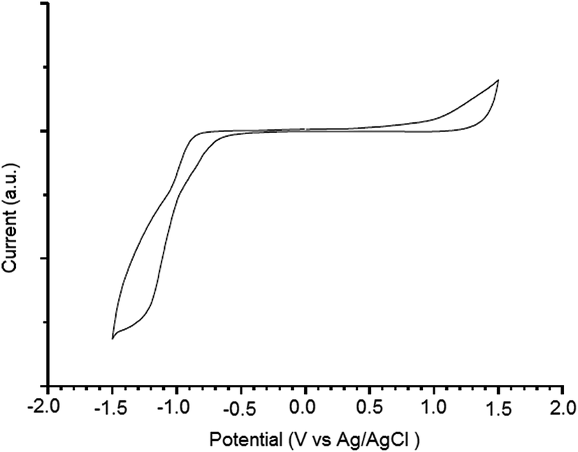 | ||
| Fig. 4 Fig. 2 Cyclic voltammograms of PTBTfBTzSi film casted on platinum working electrode in 0.1 M Bu4NPF6/acetonitrile at 100 mV s−1, potential vs. Ag/Ag+. | ||
The HOMO and LUMO energy levels of PTBTfBTzSi are −5.38 and −3.67 eV, respectively. The low lying HOMO energy level of PTBTfBTzSi is beneficial for achieving high Voc of BHJ-PSCs. The LUMO offset between the PTBTfBTzSi and PC71BM is greater than 0.3 eV, which is the generally established for minimum driving force to achieve efficient separation of the exciton into free charge carriers.
The normalized absorption spectrum of PTBTfBTzSi:PC71BM blend film is shown in Fig. 5. It can be seen from this figure that absorption spectrum of PTBTfBTzSi:PC71BM showed two distinct absorption bands in the shorter and higher wavelength regions, corresponds to the absorption spectra of PC71BM and PTBTfBTzSi, respectively, indicating that both PTBTfBTzSi and PC71BM contribute to the photogeneration of charge carriers and thereby photocurrent of the PSC.
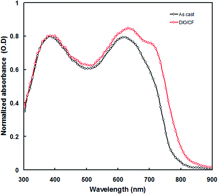 | ||
| Fig. 5 Normalized absorption spectra of PTBTfBTzSi:PC71BM (1:2) cast from CF and DIO/CF solvents. | ||
To investigate the effective exciton dissociation in the BHJ layer, the photoluminescence (PL) spectra of pristine PTBTfBTzSi and PTBTfBTzSi:PC71BM films were measured. The excitation wavelength is the maximum absorption peak of the PTBTfBTzSi thin film which is 620 nm. As shown in Fig. 6, the pristine PTBTfBTzSi film showed a strong PL emission peak at 734 nm and this peak is strongly quenched (83%) when PTBTfBTzSi is mixed with PC71BM, which indicates there is an effective charge transfer from PTBTfBTzSi to PC71BM. Moreover, when the PTBTfBTzSi:PC71BM film is processed from DIO/CF, the PL is further quenched (91%) indicates that the charge transfer from PTBTfBTzSi to PC71BM is more effective than CF cast blend film may be due to the change in the morphology of the active layer and will be discussed in the later part of discussion.
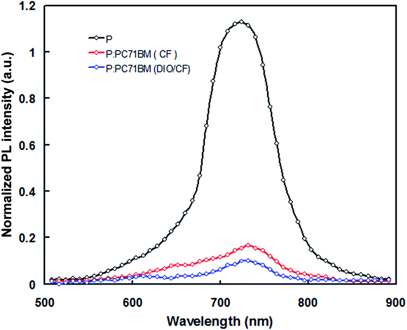 | ||
| Fig. 6 PL spectra of pristine PTBTfBTzSi (black color), PTBTfBTzSi:PC71BM cast from CF (red color) and PTBTfBTzSi:PC71BM cast from DIO/CF (blue color) thin films. | ||
3.3. Photovoltaic properties
We have used PTBTfBTzSi as donor along with PC71BM as acceptor for BHJ-PSCs with conventional structure ITO/PEDOT:PSS/PTBTfBTzSi:PC71BM/PFN/Al. First of all, the BHJ active layer was optimized by adjusting the weight ratios of PTBTfBTzSi and PC71BM in blend using CF as solvent and the photovoltaic parameters are summarized in Table 1. We found that the weight ratio of 1:1.5 at a concentration of 14 mg mL−1, gives the best photovoltaic performance. The current–voltage (J–V) characteristics of the devices under illumination are shown in Fig. 7a. The photovoltaic parameters, i.e. short circuit current (Jsc), open circuit voltage (Voc), fill factor (FF) and power conversion efficiency (PCE) are complied in Table 2. The PSC based on the optimized PTBTfBTzSi:PC71BM active layer processed with CF showed overall PCE of 4.95% with Jsc = 9.53 mA cm−2, Voc = 0.98 V and FF = 0.53. Although the Voc of the PSC is quite high, but the poor value of PCE is due to the low values of both Jsc and FF, may be attributed to the both poor nanoscale morphology of the active layer and as well as charge transport. The incident photon to current conversion efficiency (IPCE) spectrum of the PSCs is shown in Fig. 7b. The IPCE spectrum of the PSC is closely resembles with the absorption spectrum of the PTBTfBTzSi:PC71BM thin film (as shown in Fig. 3) indicating that the both PC71BM and PTBTfBTzSi contribute to the exciton generation and thereby the photocurrent generation.
| Weight ratio | Jsc (mA cm−2) | Voc (V) | FF | PCE (%) |
|---|---|---|---|---|
| 1:0.5 |
6.08 | 0.98 | 0.45 | 2.68 |
| 1:1 |
8.34 | 0.96 | 0.48 | 3.84 |
| 1:1.5 |
9.53 | 0.98 | 0.53 | 4.95 |
| 1:2 |
9.21 | 0.98 | 0.51 | 4.60 |
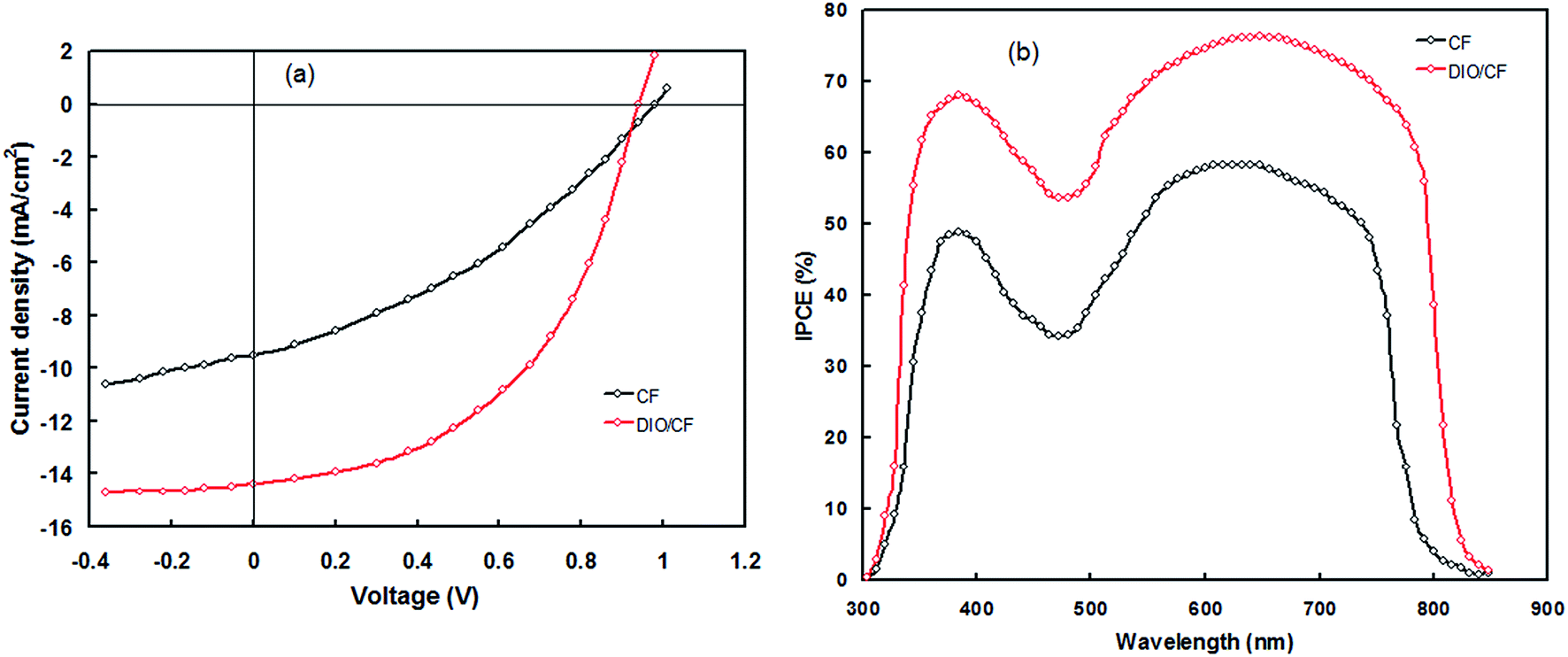 | ||
| Fig. 7 (a) Current–voltage (J–V) characteristics under illumination (100 mW cm−2, AM1.5 G) and (b) IPCE spectra of the bulk heterojunction polymer solar cells based on PTBTfBTzSi:PC71BM (CF cast) and PTBTfBTzSi:PC71BM (DIO/CF cast) active layers. | ||
:1.5) active layers processed under different conditions
In order to improve the PCE of the PSC we have adopted solvent additive (DIO as solvent additive) method, as reported in literature.15 We have varied the concentration for DIO in the host CF solvent (from 0 to 3.5 v%) and found the 3 v% DIO gives the best photovoltaic performance. The J–V characteristics under illumination and IPCE spectra of the PSC based on the active layer processed with DIO 3 v%/CF is shown in Fig. 7a and b, respectively and the photovoltaic parameters are compiled in Table 2. The PCE value is significantly improved to 8.91% with Jsc = 14.36 mA cm−2, Voc = 0.94 V and FF = 0.66. As shown in Fig. 7b, the values of IPCE across the entire wavelength region for PSC based on DIO/CF processed active layer are higher than that of CF cast counterpart. Moreover, the IPCE response of PSCs based on the active layer cast from DIO/CF is wider than that of CF based counterpart and also closely resembles with the absorption spectra of the active layer. The Jsc values estimated from the integration of IPCE spectra are about 9.41 mA cm−2 and 14.23 mA cm−2, respectively for the PSCs cast from CF and DIO/CF, respectively, which are well matched with the values extracted from the J–V characteristics under illumination of the corresponding PSCs.
The enhancement in the PCE of the PSC processed with DIO/CF is mainly due to the higher values of Jsc and FF. The value of Jsc depends upon the light harvesting efficiency (LHE) of the active layer employed in the PSC. As can be seen from the Fig. 5, the absorption of PTBTfBTzSi:PC71BM processed with DIO/CF (particularly the ICT band of PTBTfBTzSi) is higher than that of CF processed film and also red-shifted, indicating that the LHE of the active layer based on DIO/CF cast is enhanced as compared to that of CF cast counterpart. The light harvesting efficiency (ηA) of the blend films was estimated using following expression.16
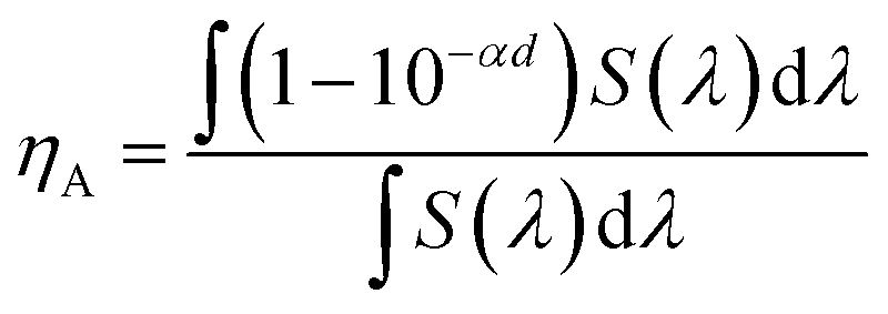
To further understand the enhancement in the Jsc and FF of the PSC based on the active layer processed with DIO/CF as compared to CF processed counterpart, we examined the dependence of Jsc and Voc with illumination intensity (Pin). Fig. 8a represents the variation of Jsc with Pin in double logarithmic scale and can be expressed by the relationship; Jsc ∝ (Pin)γ, where γ is the recombination parameter and is related to the bimolecular recombination processes in the active layer. When the value of γ is close to the unity indicate to negligible bimolecular recombination. The estimated values of γ for CF and DIO/CF processed PSCs is about 0.91 and 0.96, respectively. This clearly indicates that the bimolecular recombination is suppressed in the PSC based on the active layer processed with DIO/CF.17 Fig. 8b shows the plots of Voc as a logarithmic function of Pin with a slope of kT/q, where k is the Boltzmann's constant, q is the elementary charge and T is the temperature. If the slope is larger than kT/q, trap assisted recombination takes place in the active layer of the device and attributed to a decreased bimolecular recombination rate. It was observed that the PSC processed with DIO/CF showed less Voc dependence on illumination intensity with a slope of 1.23kT/q compared to CF processed counterpart (1.47kT/q). Therefore, trap assisted recombination is suppressed in active layer processed with DIO/CF and therefore the DIO/CF processed PSC show less bimolecular and trap assisted recombination, leading to enhanced Jsc, FF and PCE.18
 | ||
| Fig. 8 (a) Variation of (a) Jsc and (b) Voc with Pin for the PSCs based on PTBTfBTzSi:PC71BM (CF cast) and PTBTfBTzSi:PC71BM (CF cast) active layers. | ||
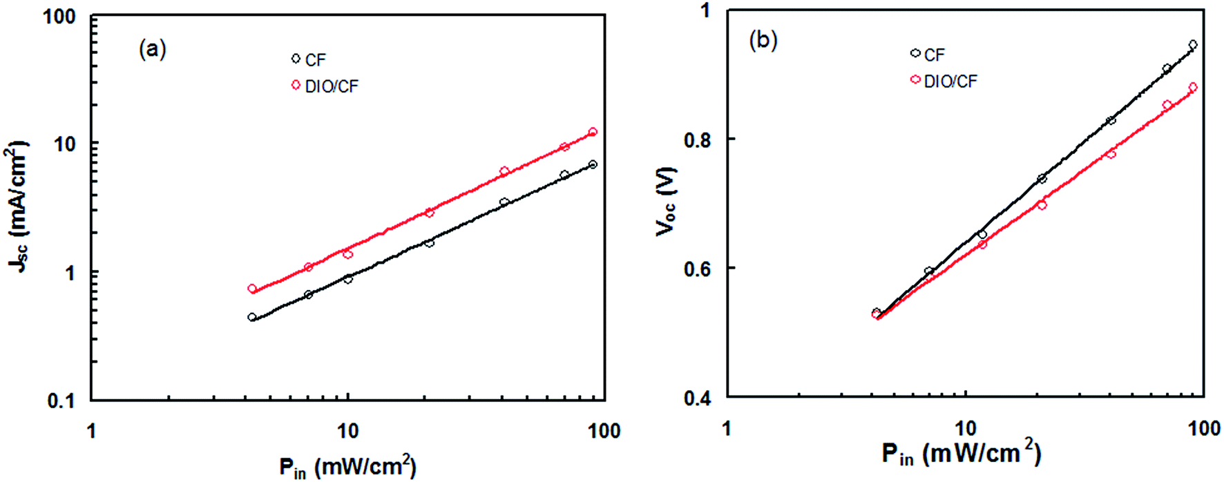
The balance charge transport between the hole and electron in the active layer is an important factor for high efficiency BHJ organic solar cells. In order to measure the charge carrier mobility (hole and electron) in the active layers processed with and without DIO, hole and electron only devices were fabricated with ITO/PEDOT:PSS PTBTfBTzSi:PC71BM/Au and ITO/Al/PTBTfBTzSi:PC71BM/Al configuration, respectively.19 The hole and electron mobilities were estimated from dark J–V characteristics and shown in Fig. 9a and b for hole and electron only devices, respectively and fitting them with the space charge limited current (SCLC) model. The hole mobilities for CF and DIO/CF processed blend film are about 6.86 × 10⁻⁵ cm2 V−1 s−1 and 1.78 × 10⁻⁴ cm2 V−1 s−1, respectively. The electron mobilities for CF and DIO/CF processed blend film are about 2.45 × 10⁻⁴ cm2 V−1 s−1 and 2.51 × 10⁻⁴ cm2 V−1 s−1, respectively. These results indicate that the hole mobility has enhanced significantly by solvent additive whereas the electron mobility remains almost same. Moreover, active layer processed with DIO/CF exhibit much more balanced charge transport (μe/μh = 1.44) as compared to CF processed counterpart (μe/μh = 3.54). This result confirms that DIO/CF processed blend film exhibits more favorable bi-continuous network pathways for hole and electron transport than that of CF counterpart.
 | ||
| Fig. 9 Dark J–V characteristics of the (a) hole only and (b) electron only devices based on PTBTfBTzSi:PC71BM (CF cast) and PTBTfBTzSi:PC71BM (DIO/CF cast) active layers. | ||
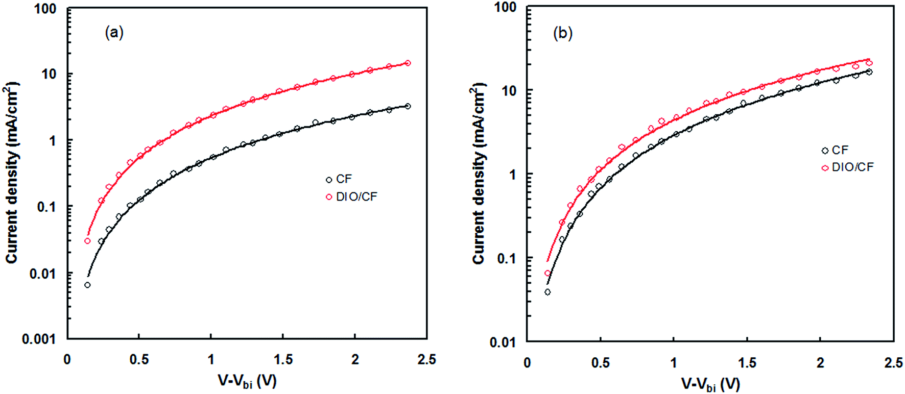
In order to get information about the exciton generation, exciton dissociation and photocurrent generation in the PSCs processed CF and DIO/CF cast active layers, the photocurrent density (Jph) (Jph = JL − JD, where JL and JD are the current densities under illumination and in dark, respectively) is plotted as a function of effective voltage (Veff) (Veff = Vo − Vapp, where Vo is the voltage when JL = JD and Vapp is applied voltage) for the PSCs20 and shown in Fig. 10. Veff is corresponds to the internal electric field of charge extraction and depends upon the internal nanoscale morphology of the active layer. In the case of PSC processed with DIO/CF, the Jph varies linearly with Veff at low voltages and gradually saturates at high value of Veff, where Jph is field independent. On the other hand, device processed with CF, also show a linear relationship at low voltages, but the Jph does not fully saturate even at high voltage of measurement, indicating that the internal electric field in this device is not sufficient for the extraction of free charge carrier. Moreover, the device based on the active layer processed with CF only, displayed square root dependence in the intermediate effective voltage region, indicating that the charge carrier transport causes the bimolecular recombination leading to the low FF.20 The maximum exciton generation rate, Gmax of the devices was estimated using expression, Jphsat = qGmaxL, where q is the electronic charge and L is the thickness of the active layer. The calculated values of Gmax in CF cast and DIO/CF cast based devices are 7.78 × 1027 m3 s−1 and 1.37 × 1028 m3 s−1, respectively. In general, Gmax in the PSCs is related to the light harvesting efficiency of the active layer21 and increased value of Gmax for DIO/CF based active layer device, clearly indicates a higher photon absorption as confirmed from the corresponding absorption spectra (Fig. 3). The charge collection efficiency (Pc) was estimated using Pc = Jsc/Jphsat at short circuit conditions and the values of Pc are 0.84 and 0.93 for the devices based on CF and DIO/CF cast active layers, respectively. Therefore, processing the active layer using DIO/CF offers significant improvement in overall PCE of PSC compared to the as cast counterpart device and related to enhanced charge collection and exciton generation rate.
 | ||
| Fig. 10 Variation of photocurrent (Jph) with effective voltage (Veff) for the PSCs based on PTBTfBTzSi:PC71BM (CF cast) and PTBTfBTzSi:PC71BM (DIO/CF cast) active layers. | ||
In order to understand the enhancement in the Jsc, FF and PCE of the PSC for the DIO/CF processed active layer compared to CF processed active layer counterpart, we have investigated the molecular ordering and the crystallinity of pristine PTBTfBTzSi film using the X-ray diffraction (XRD) pattern and shown in Fig. 11. The pristine PTBTfBTzSi showed a (100) diffraction peak at 2θ = 4.67° corresponding to the lamellar distance of 2.23 nm and a broad diffraction (010) peak was observed at 2θ = 22.45° corresponds to the fact to face π–π stacking distance of 0.38 nm. The crystalline coherence length (Lc) for pristine PTBTfBTzSi, is estimated from the Scherrer equation22 are 4.45 nm and 2.33 nm for lamellar and π–π staking, respectively. The XRD patterns of the PTBTfBTzSi:PC71BM cast from CF and DIO/CF are also shown in Fig. 11. It can be seen from this figure that the both the film showed two diffraction peaks centered at same 2θ values as observed for pristine PTBTfBTzSi, but the intensity of (100) and (010) diffraction peaks is reduced as compared to pristine PTBTfBTzSi, indicating that the crystallinity of the PTBTfBTzSi in the blend was reduced with the incorporation of PC71BM. However, an additional diffraction peak at 2θ = 18.45° was observed corresponding to the PC71BM. However, when the blend film is processed from the DIO/CF, the intensity of the (100) diffraction peak is increased. The calculated values of lamellar Lc for CF and DIO/CF blend film are 3.21 and 4.62 nm, respectively whereas Lc values of for π–π stacking for CF and DIO/CF are 1.83 and 2.42 nm, respectively. These results confirm that DIO/CF processed film has improved molecular ordering and crystallinity that are favorable photovoltaic performance.
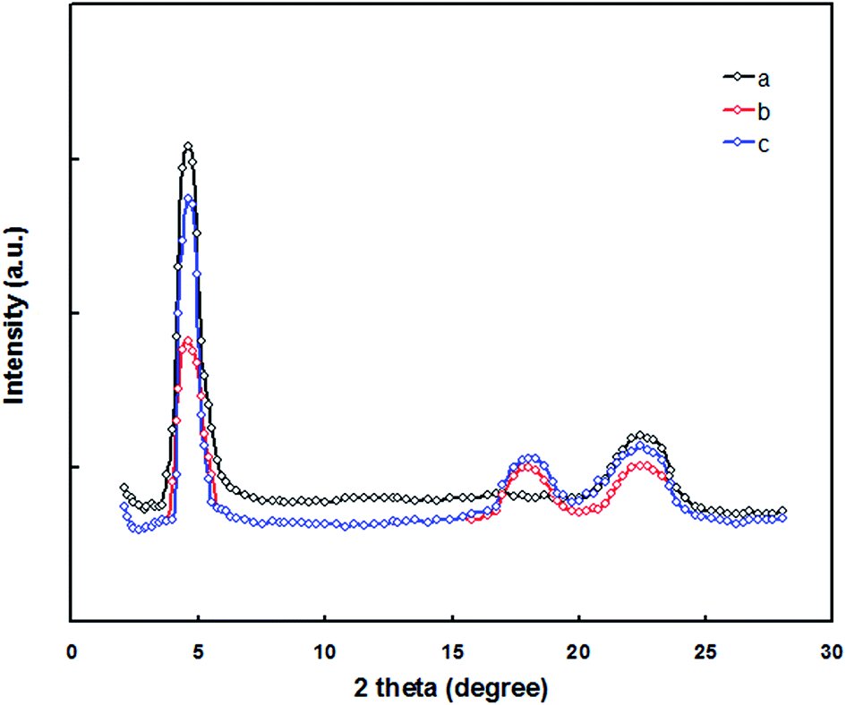 | ||
| Fig. 11 XRD patterns of (a) pristine PTBTfBTzSi, (b) PTBTfBTzSi:PC71BM (CF cast) and (c) PTBTfBTzSi:PC71BM (DIO/CF cast) thin films. | ||
Transmission electron microscopy (TEM) was used to get information about the nanoscale morphology of the active BHJ layer processed with CF and DIO/CF and shown in Fig. 12. When the active layer is processed with CF, large aggregations were observed and can reduce the degree of exciton dissociation and increase the recombination which lowers the Jsc and FF. On the other hand, when blend film processed with DIO/CF, its morphology changed. The domain size of donor and acceptor reduces in the range of 15–20 nm, which is favorable for exciton dissociation and charge transport.
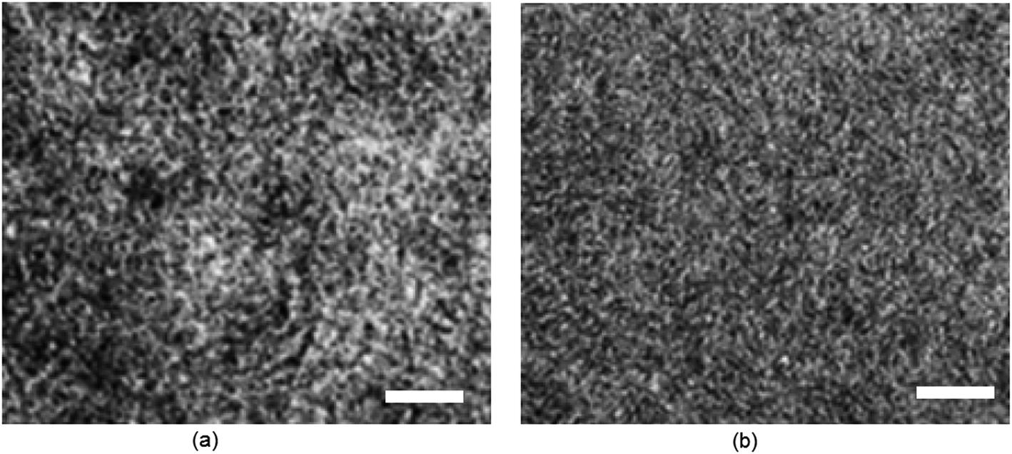 | ||
| Fig. 12 TEM images of (a) PTBTfBTzSi:PC71BM (CF cast) and (b) PTBTfBTzSi:PC71BM (DIO/CF cast) thin films with scale bar 200 nm. | ||
A key factor for the improvement in the PCE of PSC is the minimization of photon energy loss (Eloss), which is defined as Eloss = Eoptg − Voc.23 In most of the PSCs based on fullerene acceptors the Eloss is in the range of 0.7–1.0 eV is relatively very large in comparison to inorganic solar cells. We have achieved Eloss of 0.59 eV, for the optimized PSC, attributed to the low value of LUMO offset (ΔELUMO) (0.47 eV) between PTBTfBTzSi and PC71BM and also greater than the exciton binding energy (0.3 eV), to ensure the efficient exciton dissociation.24
4. Conclusions
In summary, we have synthesized a D1–A1–D1–A2–D2–A2 conjugated copolymer, PTBTfBTzSi consisting of contains two acceptors i.e. BT (A1) flanked with two thiophene (D1) and fluorinated benzotriazole (fBTz) (A2) and additional donor DTS (D2) and investigated its and used it as donor along donor along PC71BM as acceptor for solution processed BHJ PSCs. The PSS based on PTBTfBTzSi:PC71BM (1:1.5) active layer processed with DIO (3 v%)/CF showed overall PCE of 8.91% with Jsc = 14.36 mA cm−2, Voc = 0.94 V and FF = 0.66 and a low energy loss of 0.59 eV. This is the lowest values among the PSCs based on fullerene based acceptors to the best our knowledge and is the novelty of the present work. This indicates that employing two acceptors units with different electron withdrawing ability in the copolymer backbone is an effective strategy for achieving the high PCE with both fullerene and non-fullerene with low energy loss.
Conflicts of interest
There are no conflicts to declare.Acknowledgements
The reported study was funded by RFBR according to the research project No. 17-53-53198.References
- (a) L. T. Dou, Y. S. Liu, Z. R. Hong, G. Li and Y. Gang, Chem. Rev., 2015, 115, 12633 CrossRef CAS PubMed; (b) Y. F. Li, Acc. Chem. Res., 2012, 45, 723 CrossRef CAS PubMed; (c) K. Zhang, Z. Hu, C. Sun, Z. Wu, F. Huang and Y. Cao, Chem. Mater., 2017, 29, 141 CrossRef CAS; (d) C. B. Nielsen, S. Holliday, H. Y. Chen, S. J. Cryer and I. McCulloch, Acc. Chem. Res., 2015, 48, 2803 CrossRef CAS PubMed.
- (a) S. Xiao, Q. Zhang and W. You, Adv. Mater., 2016, 1601391 Search PubMed; (b) Z. Zhang and Y. Li, Sci. China: Chem., 2015, 58, 192 CrossRef CAS; (c) H. Chen, J. Hou, S. Zhang, Y. Liang, G. W. Yang, Y. Yang, L. Yu, Y. Wu and G. Li, Nat. Photonics, 2009, 3, 649 CrossRef CAS.
- (a) G. Zhang, K. Zhang, Q. Yin, X. F. Jiang, Z. Wang, J. Xin, W. Ma, H. Yan, F. Huang and Y. Cao, J. Am. Chem. Soc., 2017, 139, 2387 CrossRef CAS PubMed; (b) M. Li, K. Gao, X. Wan, Q. Zhang, B. Kan, R. Xia, F. Liu, X. Yang, H. Feng, W. Ni, Y. Wang, J. Peng, H. Zhang, Z. Liang, H. L. Yip, X. Peng, Y. Cao and Y. Chen, Nat. Photonics, 2016, 11, 85 CrossRef; (c) J. Zhao, Y. Li, G. Yang, K. Jiang, H. Lin, H. Ade, W. Ma and H. Yan, Nat. Energy, 2016, 1, 15027 CrossRef CAS; (d) D. Deng, Y. J. Zhang, J. Q. Zhang, Z. Y. Wang, L. Y. Zhu, J. Fang, B. Z. Xia, Z. Wang, K. Lu, W. Ma and Z. X. Wei, Nat. Commun., 2016, 7, 13740 CrossRef CAS PubMed.
- (a) S. Li, L. Ye, W. Zhao, S. Zhang, S. Mukherjee, H. Ade and J. Hou, Adv. Mater., 2016, 28, 9423 CrossRef CAS PubMed; (b) W. Zhao, S. Li, H. Yao, S. Zhang, Y. Zhang, B. Yang and J. Hou, J. Am. Chem. Soc., 2017, 139, 7148 CrossRef CAS PubMed.
- (a) K. H. Hendricks, G. H. J. Heintges, V. S. Gevaerts, M. M. Wienk and R. A. J. Janssen, Angew. Chem., Int. Ed., 2013, 52, 8341 CrossRef PubMed; (b) Y. H. Chao, J. F. Jheng, J. S. Wu, K. Y. Wu, H. H. Peng, M. C. Tsai, C. L. Wang, Y. N. Hsiao, C. L. Wang, C. Y. Lin and C. S. Hsu, Adv. Mater., 2014, 26, 5205 CrossRef CAS PubMed; (c) S. B. Kim, H. A. Um, H. J. Kim, M. J. Cho and D. H. Choi, Org. Electron., 2016, 31, 198 CrossRef CAS; (d) E. Y. Ko, G. E. Park, D. H. Lee, H. A. Um, J. Shin, M. J. Cho and D. H. Choi, ACS Appl. Mater. Interfaces, 2015, 7, 28303 CrossRef CAS PubMed; (e) H. J. Kim, G. E. Park, D. H. Lee, M. J. Cho and D. H. Choi, Org. Electron., 2016, 38, 256 CrossRef CAS; (f) T. Qin, W. Zajaczkowski, W. Pisula, M. Baumgarten, M. Chen, M. Gao, G. Wilson, C. D. Easton, K. Mullen and S. E. Watkins, J. Am. Chem. Soc., 2014, 136, 6049 CrossRef CAS PubMed; (g) M. Wang, H. Wang, T. Yokoyama, X. Liu, Y. Huang, Y. Zhang, T. Q. Nguyen, S. Aramaki and G. C. Bazan, J. Am. Chem. Soc., 2014, 136, 12576 CrossRef CAS PubMed; (h) Q. Tao, Y. Xia, X. Xu, S. Hedstr€om, O. B€acke, D. I. James, P. Persson, E. Olsson, O. Ingan€as, L. Hou, W. Zhu and E. Wang, Macromolecules, 2015, 48, 1009 CrossRef CAS; (i) T. Ma, K. Jiang, S. Chen, H. Hu, H. Lin, Z. Li, J. Zhao, Y. Liu, Y. M. Chang, C. C. Hsiao and H. Yan, Adv. Energy Mater., 2015, 5, 1501282 CrossRef.
- (a) H. Sirringhaus, P. J. Brown, R. H. Friend, M. M. Nielsen, K. Bechgaard, B. M. A. Langeveld-Voss, J. H. Spiering, R. A. J. Janssen, E. W. Meijer, P. Herwig and D. M. de Leeuw, Nature, 1999, 401, 685–688 CrossRef CAS; (b) I. McCulloch, M. Heeney, C. Bailey, K. Genevicius, I. Macdonald, M. Shkunov, D. Sparrowe, S. Tierney, R. Wagner, W. Zhang, M. L. Chabinyc, R. J. Kline, M. D. McGehee and M. F. Toney, Nat. Mater., 2006, 5, 328 CrossRef CAS PubMed.
- Y. Cai, L. Huo and Y. sun, Adv. Mater. DOI:10.1002/adma.201605437.
- (a) Y. Dong, X. W. Hu, C. H. Duan, P. Liu, S. J. Liu, L. Y. Lan, D. C. Chen, L. Ying, S. J. Su, X. Gong, F. Huang and Y. Cao, Adv. Mater., 2013, 25, 3683 CrossRef CAS PubMed; (b) L. Y. Lan, G. C. Zhang, Y. Dong, L. Ying, F. Huang and Y. Cao, Polymer, 2015, 67, 40 CrossRef CAS; (c) J. W. Jung, F. Liu, T. P. Russell and W. H. Jo, Adv. Energy Mater., 2015, 5, 1500065 CrossRef; (d) L. J. Huo, T. Liu, X. B. Sun, Y. H. Cai, A. J. Heeger and Y. M. Sun, Adv. Mater., 2015, 27, 2938 CrossRef CAS PubMed; (e) M. J. Zhang, X. Guo, W. Ma, H. Ade and J. H. Hou, Adv. Mater., 2015, 27, 4655 CrossRef CAS PubMed; (f) C. B. Nielsen, R. S. Ashraf, N. D. Treat, B. C. Schroeder, J. E. Donaghey, A. J. P. White, N. Stingelin and I. McCulloch, Adv. Mater., 2015, 27, 948 CrossRef CAS PubMed; (g) H. R. Li, S. Y. Sun, S. Mhaisalkar, M. T. Zin, Y. M. Lam and A. C. Grimsdale, J. Mater. Chem. A, 2014, 2, 17925 RSC; (h) C. Cabanetos, A. E. Labban, J. A. Bartelt, J. D. Douglas, W. R. Mateker, J. M. J. Fréchet, M. D. McGehee and P. M. Beaujuge, J. Am. Chem. Soc., 2013, 135, 4656 CrossRef CAS PubMed.
- S. C. Price, A. C. Stuart, L. Q. Yang, H. X. Zhou and W. You, J. Am. Chem. Soc., 2011, 133, 4625 CrossRef CAS PubMed.
- L. Lan, Z. Chen, Q. Hu, L. Ying, R. Zhu, F. Liu, T. P. Russell, F. Huang and Y. Cao, Adv. Sci., 2016, 1600032 CrossRef PubMed.
- X.-P. Xu, Y. Li, M.-M. Luo and Q. Peng, Chin. Chem. Lett., 2016, 27, 1241–1249 CrossRef CAS.
- M. Wang, D. Cai, J. Xin, W. Ma, Q. Tua and Q. Zheng, J. Mater. Chem. A, 2017, 5, 12015 CAS.
- M. L. Keshtov, S. A. Kuklin, V. S. Kochurov, N. A. Radychev, Z. Xie and A. R. Khokhlov, Dokl. Chem., 2015, 464, 231 CrossRef CAS.
- M. L. Keshtov, S. A. Kuklin, I. E. Ostapov, F. C. Chen and A. R. Khokhlov, Dokl. Chem., 2016, 470, 274–278 CrossRef CAS.
- (a) J. Lee, W. Ma, C. Brabec, J. Yuen, J. Moon, J. Kim, K. Lee, G. C. Bazan and A. J. Heeger, J. Am. Chem. Soc., 2008, 130, 3619 CrossRef CAS PubMed; (b) C. Liu, X. Hu, C. Zhong, M. Huang, K. Wang, Z. Zhang, X. Gong, Y. Cao and A. J. Heeger, Nanoscale, 2014, 6, 14297–14304 RSC.
- V. Gupta, A. Bagui and S. P. Singh, Adv. Funct. Mater., 2017, 27, 1603820 CrossRef CAS; A. Bagui and S. S. K. Iyer, IEEE Trans. Electron Devices, 2011, 58, 4061–4066 CrossRef.
- (a) S. R. Cowan, A. Roy and A. J. Heeger, Phys. Rev. B: Condens. Matter Mater. Phys., 2010, 82, 245207 CrossRef; (b) Y. Deng, W. Li, L. Liu, H. Tian, Z. Xie, Y. Geng and F. Wang, Energy Environ. Sci., 2015, 8, 585 RSC; (c) G. P. Kini, S. K. Lee, W. S. Shin, S. J. Moon, C. E. Song and J. C. Lee, J. Mater. Chem. A, 2016, 4, 18585–18597 RSC; (d) J. W. Jung, J. W. Jo, C. C. Chueh, F. Liu, W. H. Jo, T. P. Russell and A. K. Y. Jen, Adv. Mater., 2015, 27, 3310 CrossRef CAS PubMed; (e) H. Kim, B. Lim, H. Heo, G. Nam, H. Lee, J. Y. Lee, J. Lee and Y. Lee, Chem. Mater., 2017, 29, 4301 CrossRef CAS.
- K. Yao, J. J. Intemann, H. L. Yip, P. W. Liang, C. Y. Chang, Y. Zang, Z. Li, Y. Chen and A. K. Y. Jen, J. Mater. Chem. C, 2014, 2, 416 RSC.
- (a) P. W. M. Blom, M. J. M. de Jong and M. G. van Munster, Phys. Rev. B: Condens. Matter Mater. Phys., 1997, 55, R656 CrossRef CAS; (b) X. Li, W. C. H. Choy, L. Huo, F. Xie, W. E. I. Sha, B. Ding, X. Guo, Y. Li, J. Hou, J. You and Y. Yang, Adv. Mater., 2012, 24, 3046–3052 CrossRef CAS PubMed.
- (a) P. W. M. Blom, V. D. Mihailetchi, L. J. A. Koster and D. E. Markov, Adv. Mater., 2007, 19, 1551 CrossRef CAS; (b) C. M. Proctor, C. Kim, D. Neher and T. Q. Nguyen, Adv. Funct. Mater., 2013, 23, 3584 CrossRef CAS.
- V. Shrotriya, Y. Yao, G. Li and Y. Yang, Appl. Phys. Lett., 2006, 89, 063505 CrossRef.
- J. Rivnay, S. C. B. Mannsfeld, C. E. Miller, A. Salleo and M. F. Toney, Chem. Rev., 2012, 112, 5488 CrossRef CAS PubMed.
- D. Veldman, S. C. J. Meskers and R. A. J. Janssen, Adv. Funct. Mater., 2009, 19, 1939 CrossRef CAS.
- J. M. Park, D. W. Kim, H. Y. Chung, J. E. Kwon, S. H. Hong, T. M. Choi and S. Y. Park, J. Mater. Chem. A, 2017, 5, 16681 CAS.
| This journal is © The Royal Society of Chemistry 2017 |