DOI:
10.1039/C7RA08480C
(Paper)
RSC Adv., 2017,
7, 45484-45494
Highly flexible and semi-transparent Ag–Cu alloy electrodes for high performance flexible thin film heaters†
Received
1st August 2017
, Accepted 19th September 2017
First published on 25th September 2017
Abstract
We investigated the properties of thermally evaporated Ag–Cu films for application as flexible and semi-transparent electrodes for semi-transparent flexible thin film heaters (TFHs) and heat shielding films (HSFs). The effects of Ag–Cu thickness on the electrical, optical, morphological, and mechanical properties of the Ag–Cu films were investigated in detail. Based on figure of merit values calculated from the sheet resistance and optical transmittance, we optimized the thickness of the Ag–Cu alloy film. Optimized film showed no resistance changes and no cracks, even with inner and outer bending radii smaller than 5 mm, indicating sufficiently high flexibility for application in TFHs and HSFs. In addition, we measured the work function of the Ag–Cu films using Kelvin probe force microscopy to correlate the work function and surface morphology. The effect of the thickness of the Ag–Cu alloy electrodes on the saturation voltage and temperature of flexible TFHs was also investigated. In addition, we investigated the feasibility of using semi-transparent Ag–Cu alloy film in HSFs. Effective heat generation and heat shield performance of Ag–Cu alloy films suggest that the multi-functional Ag–Cu films described here can potentially be applied to create energy-efficient automobile windows and smart windows for building energy management systems.
1 Introduction
Multi-functional thin films that simultaneously function as thin film heaters (TFHs) and heat shielding film (HSFs) have attracted great interest because of the demand for functional glass for automobiles and smart windows for building energy management systems (BEMSs).1–5 To achieve simultaneous heat generation and heat shielding performance, fabrication of metal-based electrodes on flexible substrates with low sheet resistance, high transmittance, and good mechanical flexibility is critical. Although thick metal films easily generate high temperatures through resistance heating by applying power and shielding heat by absorbing near infrared (NIR) wavelengths, these films cannot be employed as smart window films due to their inherent opacity.6 Therefore, to realize multi-functional TFHs and HSFs for application to transparent glass windows or curved glass windows, the development of thin metal-based semi-transparent electrodes with low sheet resistance, smooth morphology, good mechanical flexibility, and environmentally stability is imperative. Because metal thin films with a thickness below skin depth display fairly high optical transparency, optimization of metal film thickness is very important to fabricate high quality semi-transparent metal thin film electrodes for high performance TFHs and HSFs.7 In particular, thermal response time, steady heating temperature, operating voltage, temperature uniformity, and cycling stability of TFHs are critically affected by the quality of semi-transparent electrodes.8–10 Sn-doped In2O3 (ITO) films are currently widely used as transparent electrodes for transparent TFHs because of their high optical transmittance and conductivity.8,11,12 However, the brittleness of thick ITO films and the high cost of indium limit the application of ITO films as cost-effective flexible transparent electrodes for flexible TFHs.13 Conventional ITO electrodes need to be replaced by highly flexible electrodes to realize high performance flexible TFHs and HSFs. Although several transparent electrodes made of materials such as conducting polymers, carbon (carbon nanotubes, graphene), metal nanowires, metal meshes, conductive oxides, and oxide-metal-oxides have been developed to replace ITO film in transparent TFHs, there are no reports of semi-transparent and flexible metal electrodes prepared by thermal evaporation for flexible TFHs and HSFs.1,8,14–29 In particular, flexible semi-transparent metal electrodes that can simultaneously act as heating electrodes in flexible TFHs and heat shielding electrodes in HSFs have not been investigated.
In this study, we report the electrical, optical, morphological, and mechanical properties of thermally evaporated Ag–Cu alloy films on PET substrate as a function of thickness for use as flexible and semi-transparent electrodes for flexible TFHs and HSFs. To optimize the thickness of the Ag–Cu alloy, the figure of merit (FOM) values of Ag–Cu alloy films were calculated based on sheet resistance and optical transmittance. The mechanical flexibility of the optimized Ag–Cu alloy film was investigated using a lab-designed inner bending, outer bending, and twisting test system. Furthermore, the performances of flexible TFHs and HSFs with Ag–Cu alloy electrodes were examined to explore the feasibility of using Ag–Cu alloy films as semi-transparent electrodes for high-performance flexible TFHs and HSFs.
2 Experimental
2.1 Thermal evaporation of Ag–Cu alloy films
Ag–Cu alloy films were thermally evaporated films as a function of film thickness (8 to 16 nm) on 150 μm-thick PET substrate using a lab-scale thermal evaporation system (15NNS005, NNS Vacuum). At a base pressure of 1 × 10⁻⁶ Torr, the Ag–Cu alloy films were thermally evaporated onto the PET substrate as a function of thickness; the operating conditions were applied voltage of 0.37 V, applied current of 54 A, Z-factor of 0.529, tool factor of 154%, and loading plate rotation speed of 10 rpm. The Ag–Cu alloy (90 wt% Ag–10 wt% Cu) source was loaded onto a conventional tungsten boat. The exact thickness of the Ag–Cu alloy films was controlled by a quartz thickness monitor (STM-100MF, Sycon) placed near the substrate holder.
2.2 Characterization of thermally evaporated Ag–Cu alloy films
Electrical and optical properties of the thermal evaporated Ag–Cu layer were examined using Hall measurements (HL5500PC, Accent Optical Technology) and a UV/visible spectrometer (UV 540, Unicam) as a function of film thickness. The mechanical properties of the Ag–Cu layers were evaluated using a specially designed inner and outer bending system. The outer bending test induced tensile stress on the film, whereas the inner bending test induced compressive stress. In addition, dynamic fatigue bending and twisting tests were performed using a lab-designed cyclic bending and twisting test machine, operated at a frequency of 0.5 Hz for 10![[thin space (1/6-em)]](https://www.rsc.org/images/entities/char_2009.gif) 000 cycles. The resistance of the Ag–Cu layers was measured throughout cyclic bending. Field emission scanning electron microscopy (FESEM) was employed to investigate the surface morphology of the Ag–Cu alloy films before and after bending tests. The work function and topography of the Ag–Cu alloy films were examined using Kelvin probe force microscopy (KPFM). KPFM measurements were conducted using an atomic force microscopy (AFM) system (XE-100, Park Systems) under ambient conditions (temperature: 25.5 °C, humidity: 26%). Conductive Pt-coated Si cantilevers (NSG 10/Pt, NT-MDT) were used for both work function and topography measurements. The work function of the tip was calibrated with highly ordered pyrolytic graphite (HOPG, SPI Supplies).
000 cycles. The resistance of the Ag–Cu layers was measured throughout cyclic bending. Field emission scanning electron microscopy (FESEM) was employed to investigate the surface morphology of the Ag–Cu alloy films before and after bending tests. The work function and topography of the Ag–Cu alloy films were examined using Kelvin probe force microscopy (KPFM). KPFM measurements were conducted using an atomic force microscopy (AFM) system (XE-100, Park Systems) under ambient conditions (temperature: 25.5 °C, humidity: 26%). Conductive Pt-coated Si cantilevers (NSG 10/Pt, NT-MDT) were used for both work function and topography measurements. The work function of the tip was calibrated with highly ordered pyrolytic graphite (HOPG, SPI Supplies).
2.3 Fabrication and evaluations of TFHs and HSFs
To demonstrate the feasibility of the Ag–Cu alloy films as a semi-transparent electrode for TFHs and HSFs, TFHs with a size of 25 × 25 mm2 were fabricated (ESI Fig. S1†). To apply power to the semi-transparent TFHs, two-terminal side Ag contacts were sputtered on the edge of the semi-transparent Ag–Cu layer film. DC voltage was supplied by a power supply (OPS 3010, ODA technologies) to the Ag–Cu based TFHs through an Ag contact electrode at the film edge. The temperature of TFHs was measured using a thermocouple mounted on the surfaces of the TFHs and an IR thermal imager (A35sc, FLIR). To investigate the performance of Ag–Cu alloy-based HSFs, we irradiated conventional glass substrate with a halogen lamp and measured the surface temperature of the glass substrate using an IR thermometer (62-MAX, Fluke) with or without screening the halogen lamp using semi-transparent Ag–Cu films.
3 Results and discussion
Fig. 1a shows a schematic of the thermal evaporation process used to fabricate semi-transparent Ag–Cu alloy films on flexible PET substrate. The Ag–Cu films were evaporated as a function of Ag–Cu thickness onto bare flexible PET substrate attached to a cooling substrate holder at a temperature of 16.8 °C; the operating conditions were 0.37 V and 54 A. During thermal evaporation of the Ag–Cu alloy films, the PET substrate was constantly rotated at a speed of 10 rpm to ensure a uniform Ag–Cu layer thickness. Fig. 1b shows semi-transparent Ag–Cu alloy film with a thickness of 14 nm and semi-transparent flexible TFHs. Because the thickness of Ag–Cu film is similar to the skin depth of Ag (13 nm), the Ag–Cu film had a bluish color and was semi-transparent.30 The Kyung Hee University insignia behind the Ag–Cu/PET sample was clearly visible due to the high transparency of the Ag–Cu film.
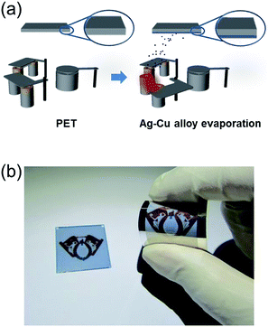 |
| | Fig. 1 (a) Schematic of the thermal evaporation process used to fabricate flexible and semi-transparent Ag–Cu alloy films on a flexible PET substrate. (b) Photograph of the semi-transparent Ag–Cu alloy film with a bluish color and a curved TFH with Ag edge contact electrodes. | |
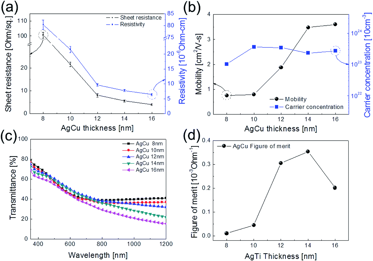
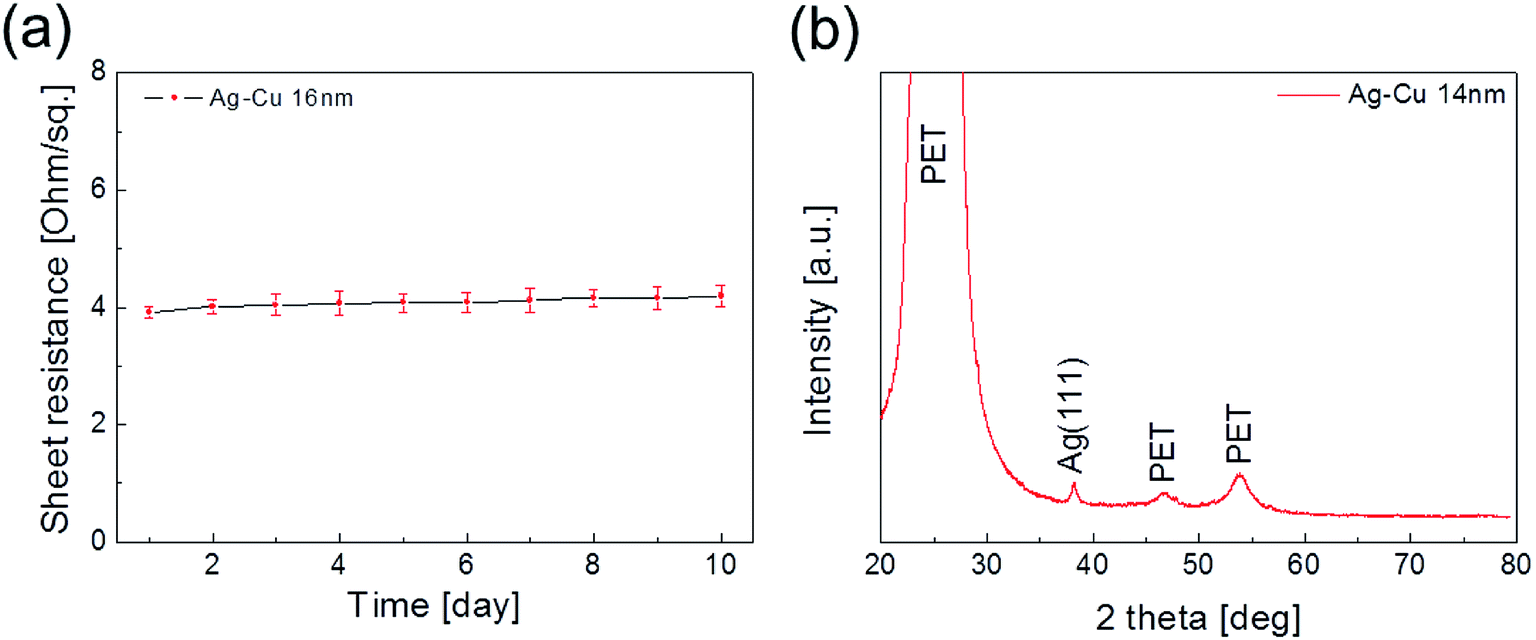
Fig. 2a and b show Hall measurement results of the Ag–Cu alloy films as a function of film thickness (8 to 16 nm). The Ag–Cu alloy film less than 8 nm thick did not show electrical conductivity due to disconnected Ag–Cu islands in the initial growth region. As we reported previously, a sputtered Ag layer on oxide film tends to agglomerate and form disconnected islands in the initial growth region due to the high surface energy of Ag atoms.31 However, further increases in Ag–Cu alloy film thickness led to connection of islands and a layered film, which acted as a conducting path. Therefore, Ag–Cu alloyed film thicker than 8 nm started to show resistivity and sheet resistance. The resistivity of Ag–Cu films decreased significantly from 3.10 × 10⁻⁵ Ohm cm to 6.39 × 10⁻⁶ Ohm cm due to the improved connectivity of the Ag–Cu alloy layer. Fig. 2b shows the mobility and carrier concentration of the Ag–Cu alloy films as a function of film thickness. An increase in film thickness led to an increase in carrier mobility due to the improved connectivity of the Ag–Cu layer. However, Ag–Cu films showed a similar carrier concentration regardless of film thickness. Therefore, we attributed the decreased resistivity of the Ag–Cu layer to an increase in carrier mobility. As discussed by Roh et al., Cu in the Ag–Cu–Pd alloy diffuses to the surface of Ag film and decreases surface diffusion of the Ag film.29 This decreased surface diffusion improves the thermal stability of Ag film. Because of the thermal stability conferred by Cu, we employed Ag–Cu alloy film as a semi-transparent electrode for flexible TFHs. Fig. 2c shows the optical transmittance of the Ag–Cu alloy film in the visible wavelength region as a function of Ag–Cu alloy film thickness. Because of the thinness of the Ag–Cu alloy film, all films demonstrated semi-transparency above 50% at a wavelength of 550 nm. The 14 nm-thick Ag–Cu alloy film had an optical transmittance of 53.62% at 550 nm. Increasing the thickness of the Ag–Cu layer from 8 to 16 nm resulted in a significant decrease in the optical transmittance of Ag–Cu alloy films in the NIR region due to reflection of this wavelength by the Ag–Cu alloy layer. Based on the sheet resistance (Rs) and transmittance (T) values of the Ag–Cu alloy films at a wavelength of 550 nm, we calculated figure of merit (FOM = T10/Rs) values as a function of thickness to optimize film thickness for a semi-transparent electrode, as shown in Fig. 2d.33 Due to low sheet resistance and high optical transmittance, the 14 nm-thick Ag–Cu alloy film showed the highest FOM value (3.5 × 10⁻⁴ Ω−1). Therefore, we chose the optimum thickness of the thermal evaporated Ag–Cu alloy film as 14 nm, which is similar to skin depth of light.30 Table 1 compared the FOM values of the evaporated Ag–Cu alloy films, several semi-transparent metals and ITO electrodes. For comparison, we prepared the several thermal evaporated semi-transparent electrode (Ag, AgPdCu, Al–Cu) with same thickness and sputtered ITO electrode except Cu–Ni film.34 Compared to the other semi-transparent metal electrodes, the Ag–Cu alloy film showed higher FOM values due to its higher optical transmittance. To investigate the stability of Ag–Cu alloy film, we measured the sheet resistance change as a function of time as shown in Fig. 3a. The evaporated Ag–Cu alloy films showed a constant sheet resistance with increasing time indicating outstanding stability against ambient. In general, Cu films or Cu nanoparticles easily react with oxygen atoms in ambient and easily form Cu–O phases on the surface.35 However, the Ag–Cu alloy films showed a constant sheet resistance regardless of time because the contents of the Cu element in the evaporated Ag–Cu alloy is fairly low. The preferred Ag (111) peak (2θ = 38.22°) in X-ray diffraction plot of the Ag–Cu (14 nm)/PET sample (Fig. 3b) indicates the low content of Cu element in the evaporated Ag–Cu alloy films.
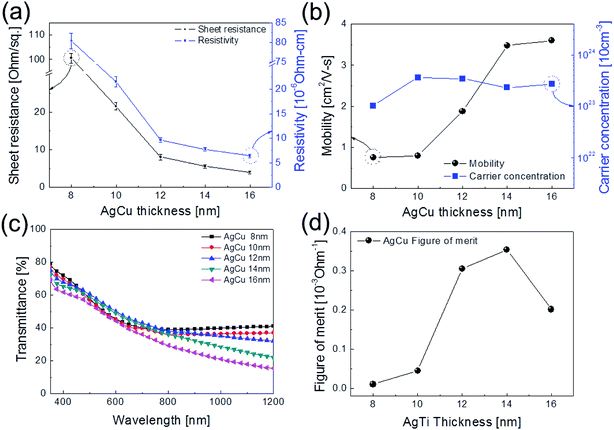 |
| | Fig. 2 (a) Sheet resistance, resistivity, (b) mobility, and carrier concentration of thermal evaporated Ag–Cu alloy films on PET substrates with increasing thickness from 8 to 16 nm. (c) Optical transmittance of Ag–Cu alloy films in the visible wavelength region as a function of increasing film thickness. (d) Figure of merit (FOM) values of Ag–Cu alloy films calculated from sheet resistance (Rs) and optical transmittance (T) values at a wavelength of 550 nm. | |
Table 1 Comparison of figure of merit values of the evaporated Ag–Cu alloy film, semi-transparent metal films and sputtered ITO films
| Material |
Ag–Cu |
Ag |
AgPdCu |
Al–Cu |
Cu–Ni |
ITO |
| Rsh [Ohm sq.−1] |
5.54 |
7.941 |
3.37 |
8.45 |
16 |
21 |
| Transmittance [%] |
53.62 |
43.76 |
46.91 |
18.39 |
57 |
86 |
| Figure of merit [10−3 Ω−1] |
0.35 |
0.03 |
0.15 |
0.000005 |
0.23 |
10.54 |
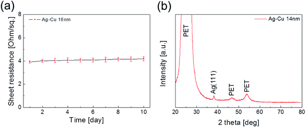 |
| | Fig. 3 (a) Change of sheet resistance of Ag–Cu alloy film in PET substrate over time. (b) XRD plot of evaporated Ag–Cu alloy film. | |
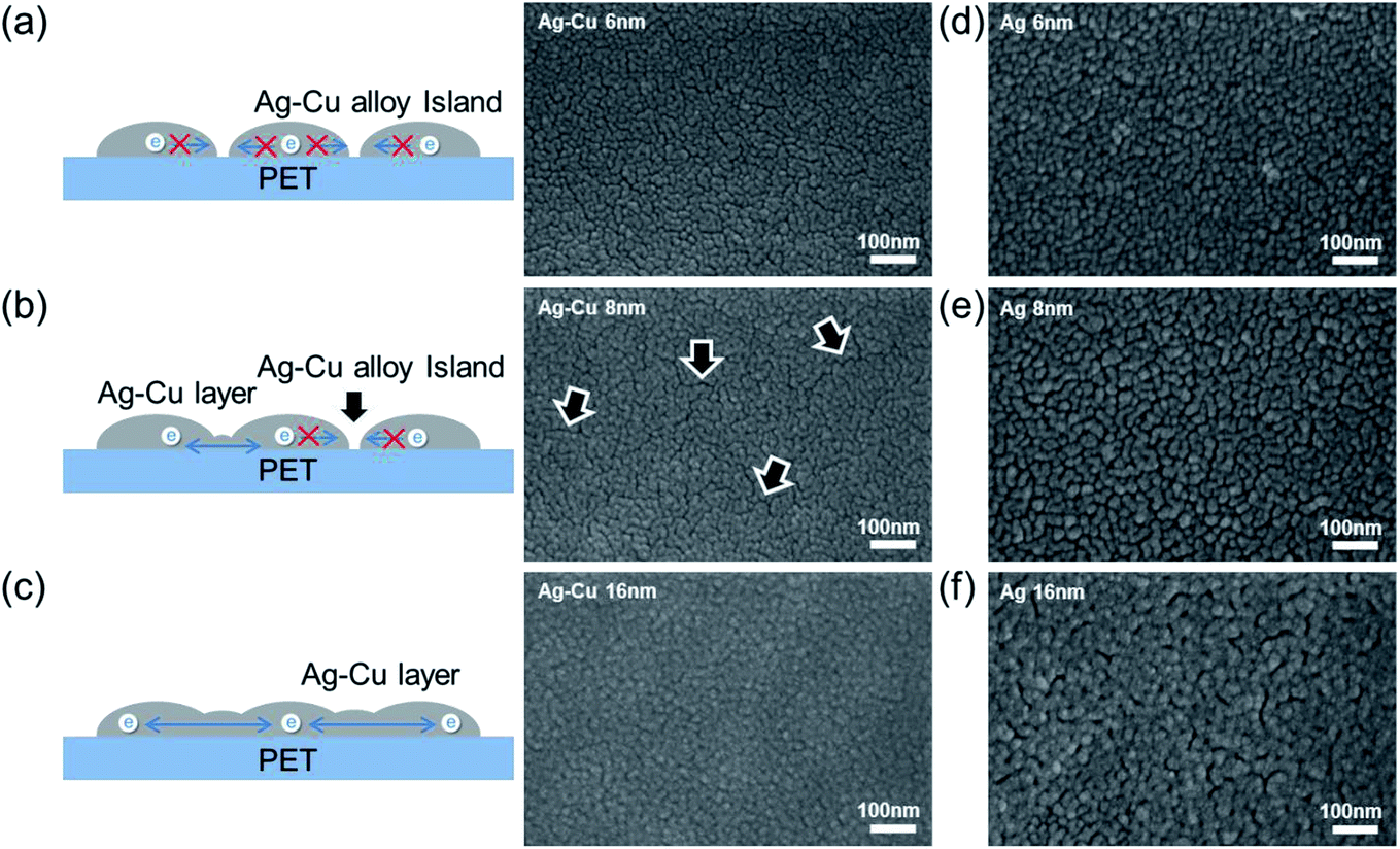
Fig. 4 shows surface FESEM images of 6, 8, and 16 nm-thick Ag–Cu alloy and bare Ag films evaporated on PET substrates. As expected from the sheet resistance of Ag–Cu alloy films in Fig. 2a, the connectivity of Ag–Cu alloy films was critically dependent on film thickness. Surface FESEM images obtained for the 6 nm-thick Ag–Cu alloy layer showed an island-shaped Ag–Cu layer caused by severe agglomeration of the Ag–Cu alloy atoms. As illustrated to the right in Fig. 4a, the unconnected Ag–Cu alloy prevented effective conduction of carriers and reduced carrier mobility. Because the 6 nm-thick Ag–Cu alloy consisted of unconnected islands, it did not show sheet resistance or resistivity because of the absence of an effective conduction path, as expected (Fig. 2a). However, the 8 nm-thick Ag–Cu alloy film showed improved connectivity due to connection of the Ag–Cu islands. Due to a decrease in surface diffusion, the Ag–Cu alloy film showed well-connected islands, even at a thickness of 8 nm.32 However, some regions, indicated by the arrows, remained unconnected, and this unconnected region increased the resistivity of the Ag–Cu alloy film (Fig. 4b). In case of the evaporated Ag films with a thickness of 6 and 8 nm (Fig. 4d and e), they showed unconnected Ag islands due to high surface diffusion of the evaporated Ag atoms on the PET surface. Due to formation of unconnected Ag islands, the evaporated Ag film didn't show metallic conductivity even at the 8 nm thickness unlike evaporated Ag–Cu alloy film. A further increase in Ag–Cu alloy and Ag film thickness led to a layered structure, which completely covered the PET substrate, as shown in Fig. 4c and f, and improved the connectivity of the Ag–Cu alloy film.
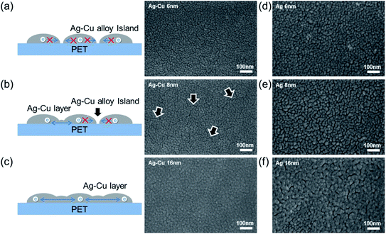 |
| | Fig. 4 Surface FESEM images and schematic cross-sectional structure of Ag–Cu alloy film on PET substrates obtained from (a) 6 nm-, (b) 8 nm-, and (c) 16 nm-thick Ag–Cu alloy films. Surface FESEM images of (d) 6 nm-, (e) 8 nm-, and (f) 16 nm-thick bare Ag films on PET substrate. | |
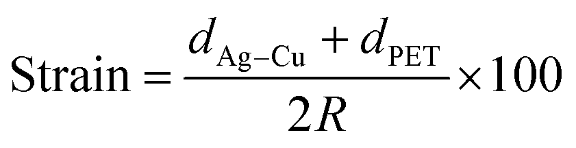
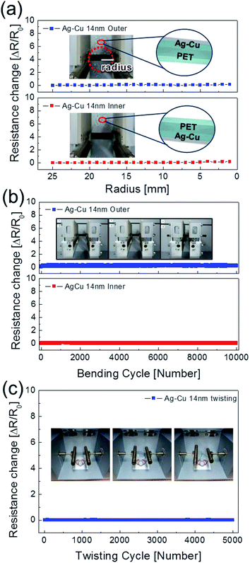
To evaluate the mechanical flexibility of optimized Ag–Cu alloy films (14 nm) as flexible electrodes for semi-transparent flexible TFHs and HSF, we measured resistance changes (ΔR) during outer and inner bending using an in-house bending test system. Fig. 5a shows the results of outer/inner bending tests of the Ag–Cu alloy films with decreasing bending radius. The outer bended Ag–Cu film experienced tensile stress, while the inner bended Ag–Cu film experienced compressive stress, as illustrated in the insets of Fig. 5a. The change in resistance of Ag–Cu alloy films can be expressed as (ΔR = R − R0)/R0, where R0 is the initial measured resistance, and R is the in situ measured resistance under substrate bending. The outer/inner bending test results showed that the 14 nm-thick Ag–Cu alloy films had a constant resistance change (ΔR) until the bending radius of 1 mm (limit of our bending test system) due to the high flexibility of the Ag–Cu alloy film. The following equation can be used to calculate the peak strain for a curved Ag–Cu alloy film with decreasing bending radius:36
| |
 | (1a) |
 |
| | Fig. 5 (a) Outer and inner bending tests of the 14 nm-thick Ag–Cu alloy film with decreasing bending radius. (b) Dynamic fatigue tests of the 14 nm-thick Ag–Cu alloy film with increasing bending cycles. (c) Twisting test of the Ag–Cu alloy film with repeated twisting cycles. Inset pictures demonstrate outer/inner bending of samples, dynamic bending steps, and twisting steps. | |
Here, dAg–Cu and dPET are the thickness of the Ag–Cu alloy film and the PET substrate, respectively. Bending of the 14 nm-thick Ag–Cu alloy on a 150 μm-thick PET substrate to a bending radius of 1 mm resulted in a peak strain of 7.5%. This flexibility is sufficient for fabrication of highly flexible TFHs and HSFs. Fig. 5b shows the dynamic outer and inner bending fatigue test results obtained for the 14 nm-thick Ag–Cu alloy film with increasing repeated bending cycles at a fixed bending radius of 5 mm, which is acceptable for fabrication of flexible TFHs attached to a rounded glass substrate. The insets in Fig. 5b are pictures of dynamic outer/inner bending test steps with increasing bending cycles. Both dynamic outer and inner bending fatigue tests of the thermally evaporated Ag–Cu alloy film revealed no change in resistance after 10000 bending cycles, indicating that the Ag–Cu alloy film had good flexibility and stability. Fig. 5c shows the results of a dynamic twisting test of the 14 nm-thick Ag–Cu layer with increasing twisting cycles at a fixed twisting angle of 15°. The ΔR/R0 value of the Ag–Cu layer electrode was almost unchanged with increasing repeated twisting cycles. Even after 1 mm outer/inner bending of the samples, the surface of the Ag–Cu alloy was similar to that of the as-deposited Ag–Cu alloy film, confirming the good flexibility of the Ag–Cu alloy film (ESI Fig. S2†). In addition, the Ag–Cu alloy film showed a similar surface to the as-deposited sample even after 10000 dynamic outer/inner bending cycles.
Fig. 6a and b show topography images and work function maps of Ag–Cu alloy films of various thicknesses. Using a Kelvin probe force microscopy (KPFM) system, we obtained surface topography and work function data for the same region.37–40 When the thickness of the Ag–Cu alloy film increased, the work function of the Ag–Cu film increased from 4.78 to 5.06 eV. As shown in Fig. 6a and b, neither surface morphology nor roughness influenced the measured work function value, ruling out any concerns about topographic artifacts in the KPFM measurements. The standard deviation of the work function data was very small (less than 0.5%), which suggests that the Ag–Cu alloy thin film had a homogeneous composition. Table 2 summarizes the sheet resistance, optical transmittance, figure of merit, and work function values obtained for thermally evaporated Ag–Cu layers of various thicknesses.
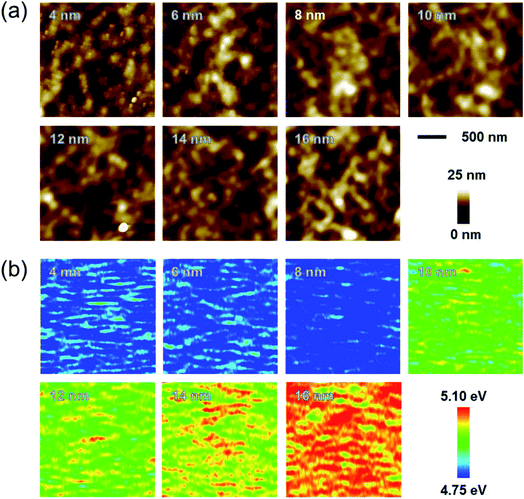 |
| | Fig. 6 (a) Topography images and (b) work function maps of Ag–Cu layers of various thicknesses ranging from 4 to 16 nm. | |
Table 2 Sheet resistance, optical transmittance, and work function of thermally evaporated Ag–Cu alloy films on PET substrate and the calculated figure of merit
| Thickness |
Sheet resistance [Ohm sq.−1] |
Transmittance550 nm [%] |
Figure of merit [10−3 Ω−1] |
Work function [eV] |
| 4 nm |
— |
42.44 |
— |
4.78 ± 0.02 |
| 6 nm |
— |
31.98 |
— |
4.75 ± 0.01 |
| 8 nm |
100.5 |
50.65 |
0.01 |
4.75 ± 0.02 |
| 10 nm |
21.5 |
49.86 |
0.04 |
4.98 ± 0.01 |
| 12 nm |
8.02 |
54.82 |
0.31 |
4.92 ± 0.01 |
| 14 nm |
5.54 |
53.62 |
0.35 |
4.96 ± 0.01 |
| 16 nm |
3.99 |
49.04 |
0.20 |
5.06 ± 0.01 |
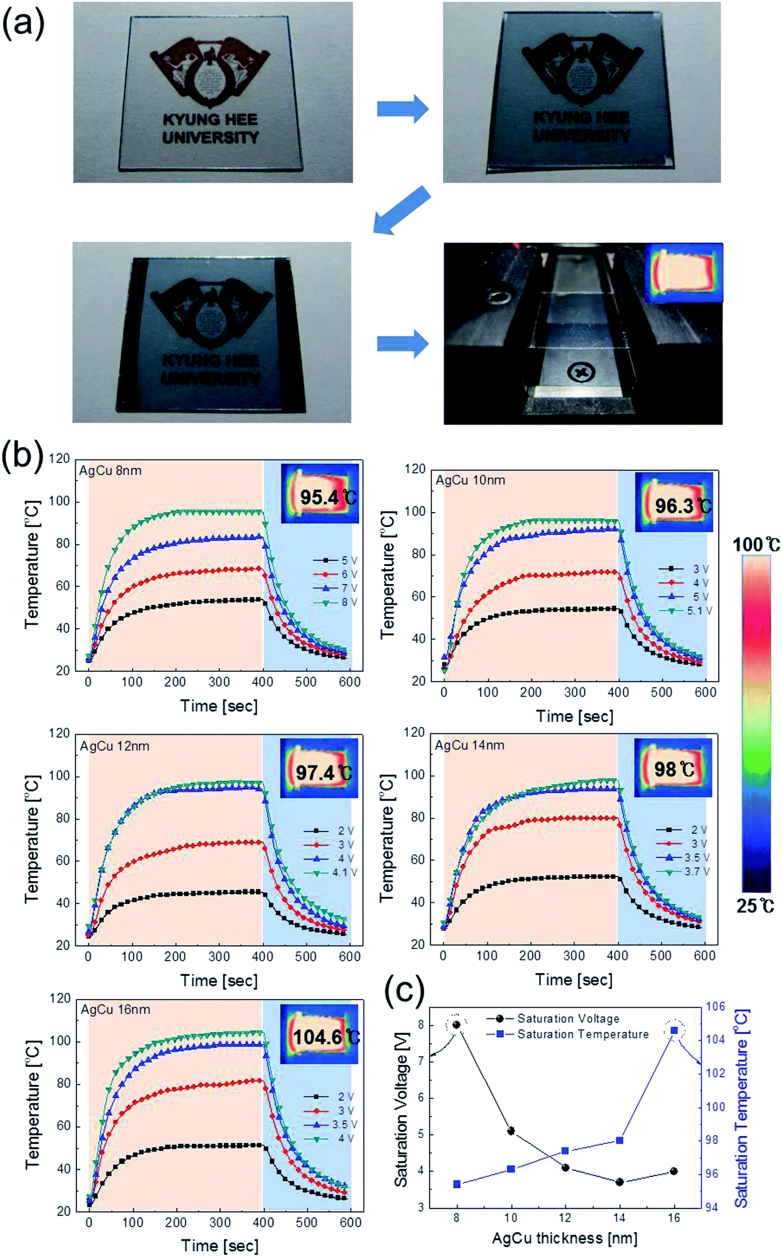
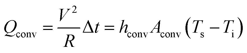
To investigate the feasibility of using thermally evaporated Ag–Cu alloy films as flexible and semi-transparent electrodes for flexible TFHs, flexible TFHs with a size of 25 × 25 mm2 were fabricated using a two-terminal Ag contact configuration. Fig. 7a shows photographs of the fabrication of flexible TFHs with semi-transparent Ag–Cu alloy electrodes. DC voltage was applied to the flexible TFHs by a power supply through sputtered Ag contact electrodes at the film edge, as shown in Fig. 7a. The temperature profile of flexible TFHs was measured by a thermocouple placed on the surface of the TFHs. Fig. 7b shows the temperature profiles of the Ag–Cu alloy film-based TFHs, plotted with respect to input voltage as a function of Ag–Cu alloy film thickness from 8 to 16 nm. When DC voltage was supplied to the Ag–Cu alloy film-based TFHs, the temperature of the all-flexible TFHs gradually increased and reached the saturation temperature. As the input voltage was increased, the temperature of the flexible TFHs increased, as shown in all of the temperature profiles. It is noteworthy that the increase in Ag–Cu alloy thickness decreased the input DC voltage to achieve a temperature of 100 °C. In the case of flexible TFHs with an 8 nm-thick Ag–Cu alloy film, 8 V of input DC voltage was necessary to achieve 95 °C. An increase in Ag–Cu alloy film thickness to 16 nm led to a significant decrease in input DC voltage to 4 V to produce a temperature greater than 100 °C. The lower input voltage of the flexible TFHs with thicker Ag–Cu film to reach a temperature of 100 °C implies efficient transduction of electric energy into Joule heating in the Ag–Cu alloy-based flexible TFHs. The sheet resistance of Ag–Cu alloy electrodes and the saturated temperature of flexible TFHs are correlated. When power (P) is applied to flexible TFHs during heating for a certain amount of time (t), the generated heat (ΔQg) is the summation of heat loss due to conduction in the substrate (Qcond), heat loss due to convection in air (Qconv), and heat loss due to radiation (Qrad) from flexible TFHs, as expressed in the following equation:8,24
| |
 | (2a) |
 |
| | Fig. 7 (a) Photographs of the fabrication process of flexible TFHs with semi-transparent Ag–Cu electrodes. (b) Temperature profile of flexible TFHs operated at different input voltages with increasing semi-transparent Ag–Cu alloy film thickness. The insets show IR images at the saturated temperature. (c) Saturation voltage and temperature of Ag–Cu alloy-based TFHs as a function of Ag–Cu thickness. | |
Here, V is the input DC voltage between the Ag contact electrodes, and T is the resistance of the TFHs. In our flexible TFH samples, heat loss due to conduction was negligible because the sample was not in contact with a good thermal conductor. In addition, heat loss caused by radiation was negligible below 100 °C because of the very low emissivity of the Ag–Cu alloy. Therefore, air convection is the main path of heat dissipation in Ag–Cu alloy-based flexible TFHs.41
| |
 | (3a) |
| |
 | (3b) |
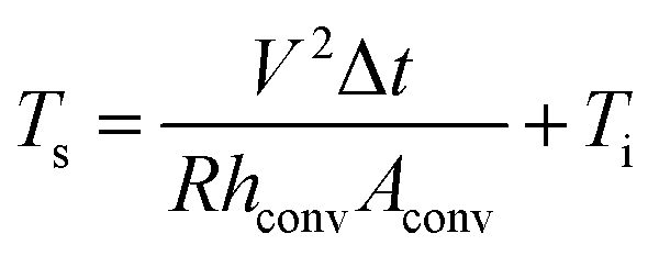
In eqn (3a) and (3b), hconv is the convective heat transfer coefficient, Aconv is the surface area, and Ts and Ti are the saturation and initial temperature, respectively. Based on these equations, it is apparent that the saturation temperature of flexible TFHs increases with increasing input DC voltage (V) and with decreasing resistance (R). Therefore, flexible and semi-transparent Ag–Cu alloy electrodes should have a low sheet resistance to realize high-performance flexible TFHs with a lower DC input voltage to achieve a temperature of 100 °C.
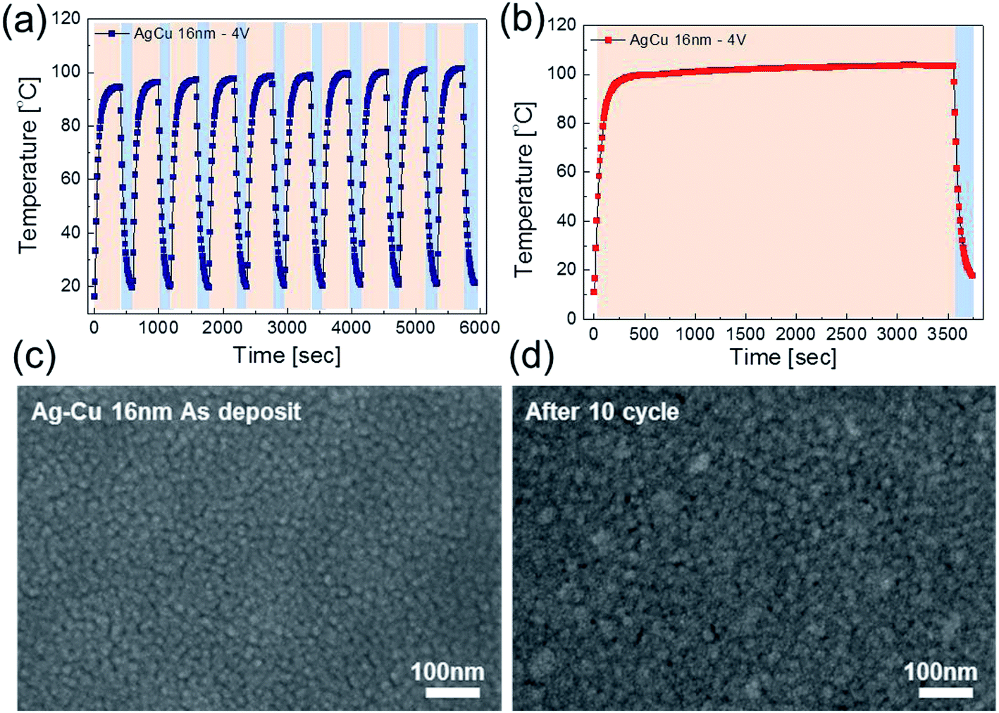
To investigate durability of the Ag–Cu alloy based TFHs, we performed repeated heating-cooling tests for 10 cycles. Fig. 8a shows the temperature profiles of the 16 nm thick-Ag–Cu alloy film-based TFHs for repeated 10 cycles. The Ag–Cu alloy films based TFHs showed an identical temperature profiles and easily reached at a saturation temperature of 100 °C when DC voltage of 4 V was applied. In addition, when the DC voltage of 4 V was supplied to Ag–Cu alloy film based TFHs for 1 hour, the TFHs keep a saturation temperature of 100 °C steady without temperature modulation as shown in Fig. 8b. The similar surface FESEM images of the Ag–Cu alloy film before and after heating in Fig. 8c and d also indicate the durability of the semi-transparent Ag–Cu alloy films as an electrode for flexible and semi-transparent TFHs. Even after 10000 times inner/outer bending cycles and 5000 times twisting cycles, the Ag–Cu-based TFHs showed identical heating performances to as-deposited Ag–Cu based TFHs (ESI Fig. S3†) indicating outstanding stability and flexibility of the thermal evaporated Ag–Cu films.
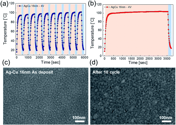 |
| | Fig. 8 (a) Temperature profiles of the Ag–Cu alloy based TFH under repeated hating and cooling for 10 cycles. (b) Temperature profile of the Ag–Cu alloy based TFHs when DC voltage of 4 V was supplied for 1 hour. Surface FESEM images of the Ag–Cu alloy film (c) before and (d) after heating for 1 hour. | |
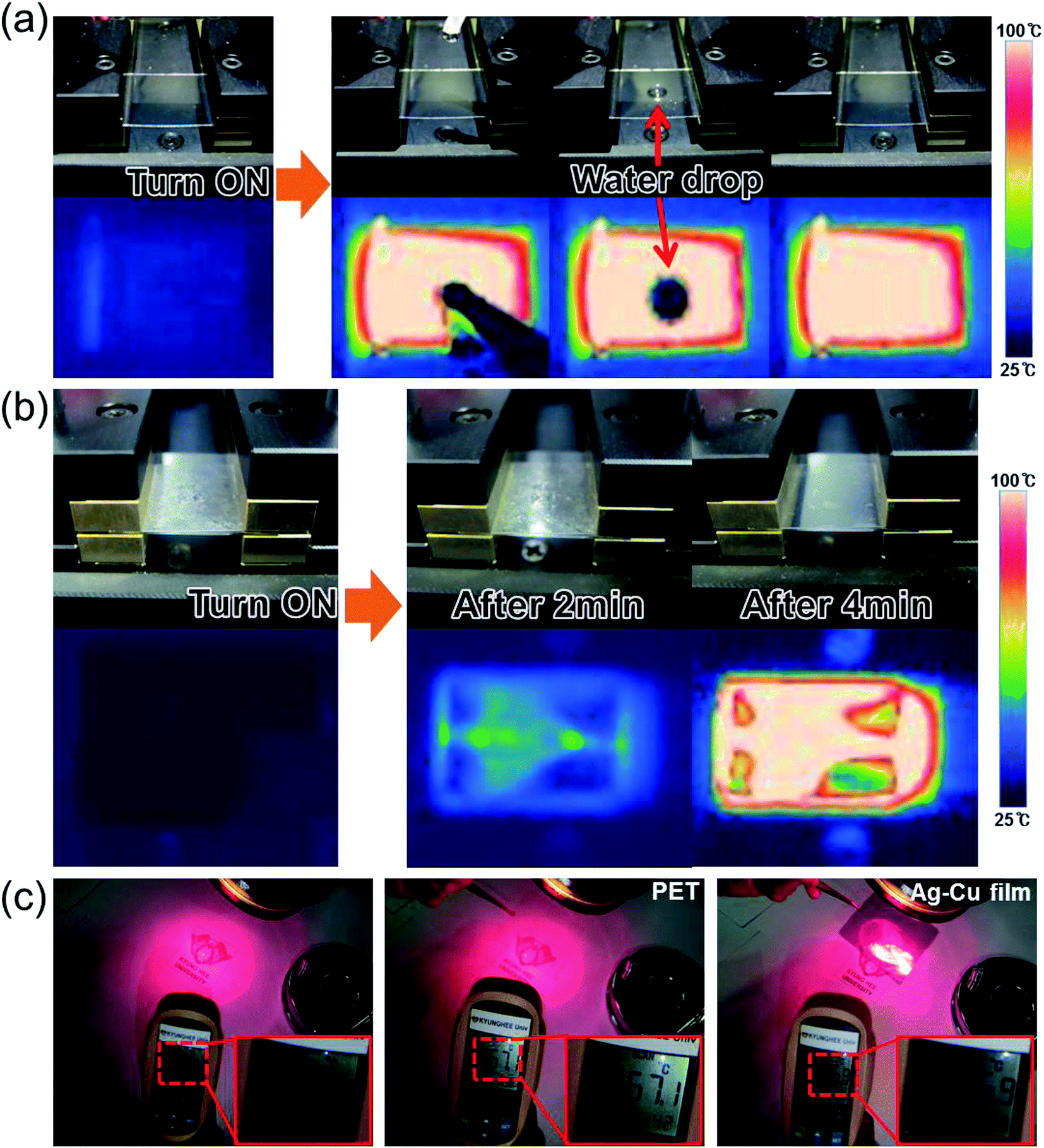
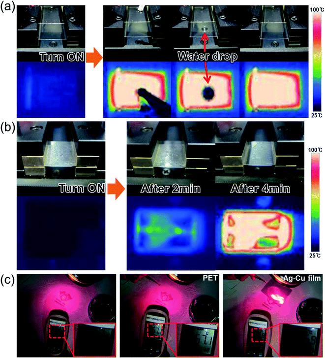
The lower DC input voltage of flexible TFHs with a thicker Ag–Cu alloy electrode confirms that flexible and semi-transparent electrodes with a lower sheet resistance are critical to obtain high-performance TFHs with a lower input DC voltage. To demonstrate the feasibility of Ag–Cu alloy film-based TFHs, a water droplet test was performed on the heated flexible TFH. Fig. 9a shows pictures of the water droplet test and IR images of the Ag–Cu-based flexible TFHs with a saturation temperature of 104.6 °C. When a DC input voltage of 4 V was supplied to the flexible TFHs, a saturation temperature of 104.6 °C was instantly achieved due to a dynamic balance between Joule heating and convection. Therefore, the water droplet disappeared almost immediately due to the high temperature of the Ag–Cu alloy film-based flexible TFHs. Fig. 9b demonstrates the defrost test of the Ag–Cu alloy-based TFHs before and after frost formation. To ensure uniform frost formation on the surface of the Ag–Cu alloy electrode, the sample was placed in a refrigerator for 60 min. At the operating voltage of 4 V, the frost on the surface of the Ag–Cu alloy electrode completely disappeared. Semi-transparent Ag–Cu alloy electrodes can also be applied to HSFs for BEMS because of their semi-transmittance in the visible wavelength region and high reflection in the NIR region, as shown in Fig. 2c. By effective shielding of heating through a semi-transparent window, total energy consumption in a building can be effectively controlled. Fig. 9c shows a heat shielding test using bare PET film and Ag–Cu alloy-coated PET film. Irradiating glass with light from a halogen lamp resulted in an increase in temperature. The surface temperature of the glass was measured by a IR thermometer (62-MAX, Fluke). Without HSF, the surface of the glass showed a temperature of 58.4 °C under halogen lamp irradiation. When the light was blocked by bare PET substrate, there was a small decrease in temperature (57.4 °C). However, when the radiation was blocked by semi-transparent Ag–Cu alloy film, the surface temperature of the glass substrate was significantly reduced from 58.4 to 36.9 °C, indicating that the semi-transparent Ag–Cu alloy electrodes were effective at shielding the substrate from heat. Therefore, the Ag–Cu alloy coated film can be used as a TFH and HSF simultaneously in automobile windows or smart windows for BEMS.
 |
| | Fig. 9 (a) Images of the water droplet test on heated flexible TFHs with an Ag–Cu alloy electrode. (b) Defrosting test results of the Ag–Cu alloy-based THFs before and after frost formation. (c) Photographs demonstrate the heat-shielding performance of the Ag–Cu alloy film. Irradiation of a glass substrate with a halogen lamp increased the temperature of the substrate to 58.4 °C. | |
Fig. 10 demonstrates promising applications of the semi-transparent Ag–Cu alloy electrode-based flexible TFHs and HSFs. They can be employed to create semi-transparent toasters (Fig. 10a), defogging/deicing windows (Fig. 10b) for automobiles, and smart windows due to their flexibility and semi-transparency. For employment in smart windows for BEMS, large-area Ag–Cu alloy films can be prepared on a PET substrate using a thermal evaporation process. For energy-efficient building, cost-effective defogging/deicing systems and heat shielding systems can be realized by using large smart windows.
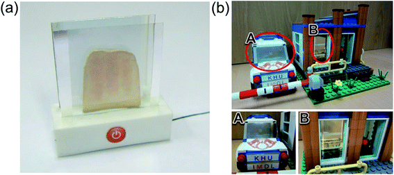 |
| | Fig. 10 Promising applications of Ag–Cu alloy film-based TFHs: (a) transparent toaster, (b) smart window for an automobile, and smart windows for BEMS. | |
4 Conclusions
We developed semi-transparent Ag–Cu alloy films for use as flexible and semi-transparent electrodes for semi-transparent flexible TFHs and HSFs. The effects of Ag–Cu thickness on the electrical, optical, and morphological properties of Ag–Cu electrodes were investigated in detail. Based on figure of merit values calculated from sheet resistance and optical transmittance measurements of Ag–Cu films, we obtained an optimized Ag–Cu alloy film with a sheet resistance of 5.54 Ohm per square, optical transmittance of 53.62%, critical bending radius of 1 mm, and work function of 4.96 eV. Below inner and outer bending radii of 1 mm, the thermally evaporated Ag–Cu alloy film showed no resistance change and no cracks, indicating sufficient flexibility for fabrication of highly flexible TFHs and HSFs. We also investigated the effect of the thickness of the Ag–Cu alloy electrodes on saturation voltage and the temperature of thin film heaters. Furthermore, we evaluated the possibility of using semi-transparent Ag–Cu alloy films as flexible HSFs due to their low optical transmittance in the NIR region. The heat generation and heat shield performance of the optimized Ag–Cu alloy film indicated that it is feasible to use Ag–Cu alloy film to create energy-efficient automobile windows, smart windows for BEMS, and energy efficient vinyl-houses.
Conflicts of interest
There is no conflicts to declare.
Acknowledgements
This work was supported by the Korea Institute of Energy Technology Evaluation and Planning (KETEP) and the Ministry of Trade, Industry & Energy (MOTIE) of the Republic of Korea (No. 20163010012200). This study also received partial support from the National Research Foundation of Korea (NRF) grant funded by the Korea government (MSIP) (No. 2015R1A2A2A01002415).
References
- S.-H. Park, S.-M. Lee, E.-H. Ko, T.-H. Kim, Y.-C. Nah, S.-J. Lee, J. H. Lee and H.-K. Kim, Sci. Rep., 2016, 6, 33868–33879 CrossRef CAS PubMed.
- L. Dai, S. Chen, J. Liu, Y. Gao, J. Zhou, Z. Chen, C. Cao, H. Luo and M. Kanehira, Phys. Chem. Chem. Phys., 2013, 15, 11723–11729 RSC.
- R. J. Mortimer, D. R. Rosseinsky and P. M. S. Monk, Electrochromic materials and devices, WILEY-VCH, New Jersey, 2015 Search PubMed.
- C. M. Lampert, Sol. Energy Mater. Sol. Cells, 1981, 6, 1–41 CrossRef CAS.
- R. Baetens, B. P. Jelle and A. Gustavsen, Sol. Energy Mater. Sol. Cells, 2010, 94, 87–105 CrossRef CAS.
- D. Michels, J. Hadeler and V. J. H. Lienhard, Exp. Heat Transfer, 1998, 11, 341–359 CrossRef CAS.
- G. Hass and J. E. Waylonis, J. Opt. Soc. Am., 1961, 51, 719–722 CrossRef CAS.
- E.-H. Ko, H.-J. Kim, S.-J. Lee, J.-H. Lee and H.-K. Kim, RSC Adv., 2016, 6, 46634–46642 RSC.
- W. Lan, Y. Chen, Z. Yang, W. Han, J. Zhou, Y. Zhang, J. Wang, G. Tang, Y. Wei, W. Dou, Q. Su and E. Xie, ACS Appl. Mater. Interfaces, 2017, 9, 6644–6651 CAS.
- S. Sorel, D. Bellet and J. N. Coleman, ACS Nano, 2014, 8, 4805–4814 CrossRef CAS PubMed.
- M. C. Çakır, D. Çalışkan, B. Bütün and E. Özbay, Sensors, 2016, 16, 1612 CrossRef PubMed.
- K. Im, K. Cho, K. Kwak, J. Kim and S. Kim, J. Nanosci. Nanotechnol., 2013, 13, 3519–3521 CrossRef CAS PubMed.
- D. R. Cairns, R. P. Witte II, D. K. Sparacin, S. M. Sachsman, D. C. Paine and G. P. Crawford, Appl. Phys. Lett., 2000, 76, 1425–1427 CrossRef CAS.
- S.-I. Na, S.-S. Kim, J. Jo and D.-Y. Kim, Adv. Mater., 2008, 20, 4061–4067 CrossRef CAS.
- H.-S. Jang, S. K. Jeon and S. H. Nahm, Carbon, 2011, 49, 111–116 CrossRef CAS.
- T. J. Kang, T. Kim, S. M. Seo, Y. J. Park and Y. H. Kim, Carbon, 2011, 49, 1087–1093 CrossRef CAS.
- Y.-H. Yoon, J.-W. Song, D. Kim, J. Kim, J.-K. Park, S.-K. Oh and C.-S. Han, Adv. Mater., 2007, 19, 4284–4287 CrossRef CAS.
- J. Kang, H. Kim, K. S. Kim, S.-K. Lee, S. Bae, J.-H. Ahn, Y.-J. Kim, J.-B. Choi and B. H. Hong, Nano Lett., 2011, 11, 5154–5158 CrossRef CAS PubMed.
- T. Kim, Y. W. Kim, H. S. Lee, H. Kim, W. S. Yang and K. S. Suh, Adv. Funct. Mater., 2013, 23, 1250–1255 CrossRef CAS.
- K. D. M. Rao and G. U. Kulkarni, Nanoscale, 2014, 6, 5645–5651 RSC.
- J. Kang, Y. Jang, Y. Kim, S.-H. Cho, J. Suhr, B. H. Hong, J.-B. Choi and D. Byun, Nanoscale, 2015, 7, 6567–6573 RSC.
- S. Ji, W. He, K. Wang, Y. Ran and C. Ye, Small, 2014, 10, 4951–4960 CrossRef CAS PubMed.
- R. Gupta, K. D. M. Rao, K. Srivastava, A. Kumar, S. Kiruthika and G. U. Kulkarni, ACS Appl. Mater. Interfaces, 2014, 6, 13688–13696 CAS.
- R. Gupta, K. D. M. Rao, S. Kirthika and G. U. Kulkarni, ACS Appl. Mater. Interfaces, 2016, 8, 12559–12575 CAS.
- D. Lordan, M. Burke, M. Manning, A. Martin, A. Amann, D. O'Connell, R. Murphy, C. Lyons and A. J. Quinn, ACS Appl. Mater. Interfaces, 2017, 9, 4932–4940 CAS.
- C. Hudaya, B. J. Jeon and J. K. Lee, ACS Appl. Mater. Interfaces, 2015, 7, 57–61 CAS.
- K. Kim, J. Kim, B. G. Hyun, S. Ji, S.-Y. Kim, S. Kim, B. W. An and J.-U. Park, Nanoscale, 2015, 7, 14577 RSC.
- B. W. An, E.-J. Gwak, K. Kim, Y.-C. Kim, J. Jang, J.-Y. Kim and J.-U. Park, Nano Lett., 2016, 16, 471–478 CrossRef CAS PubMed.
- H.-G. Im, B. W. An, J. Jin, J. Jang, Y.-G. Park, J.-U. Park and B.-S. Bae, Nanoscale, 2016, 8, 3916 RSC.
- M. J. Bloemer and M. Scalora, Appl. Phys. Lett., 1998, 72, 1676–1678 CrossRef CAS.
- K.-H. Choi, H.-J. Nam, J.-A. Jeong, S.-W. Cho, H.-K. Kim, J.-W. Kang, D.-G. Kim and W.-J. Cho, Appl. Phys. Lett., 2008, 92, 223302 CrossRef.
- H.-S. Roh, S.-H. Cho and W.-J. Lee, Phys. Status Solidi A, 2010, 207, 1558–1562 CrossRef CAS.
- G. Haacke, J. Appl. Phys., 1976, 47, 4086–4089 CrossRef CAS.
- D. S. Ghosh, R. Betancur, T. L. Chen, V. Pruneri and J. Martorell, Sol. Energy Mater. Sol. Cells, 2011, 95, 1228–1231 CrossRef CAS.
- A. Soon, M. Todorova, B. Delley and C. Stampfl, Phys. Rev. B, 2006, 73, 165424 CrossRef.
- D.-Y. Cho, K.-H. Kim, T.-W. Kim, Y.-J. Noh, S.-I. Na, K.-B. Chung and H.-K. Kim, Org. Electron., 2015, 24, 227–233 CrossRef CAS.
- M. Bieletzki, T. Hynninen, T. M. Soini, M. Pivetta, C. R. Henry, A. S. Foster, F. Esch, C. Barth and U. Heiz, Phys. Chem. Chem. Phys., 2010, 12, 3203–3209 RSC.
- S. Sadewasser, P. Jelinek, C.-K. Fang, O. Custance, Y. Yamada, Y. Sugimoto, M. Abe and S. Morita, Phys. Rev. Lett., 2009, 103, 266103 CrossRef PubMed.
- Y. Zhang, O. Pluchery, L. Caillard, A.-F. Lamic-Humblot, S. Casale, Y. J. Chabal and M. Salmeron, Nano Lett., 2015, 15, 51–55 CrossRef CAS PubMed.
- F. Long, P. Yasaei, R. Sanoj, W. Yao, P. Král, A. Salehi-Khojin and R. Shahbazian-Yassar, ACS Appl. Mater. Interfaces, 2016, 8, 18360–18366 CAS.
- D. Jung, M. Han and G. S. Lee, J. Vac. Sci. Technol. B, 2014, 32, 04E105 Search PubMed.
Footnote |
| † Electronic supplementary information (ESI) available. See DOI: 10.1039/c7ra08480c |
|
| This journal is © The Royal Society of Chemistry 2017 |
Click here to see how this site uses Cookies. View our privacy policy here. 
 Open Access Article
 This Open Access Article is licensed under a
  *a
*a