
 Open Access Article
 This Open Access Article is licensed under a Creative Commons Attribution-Non Commercial 3.0 Unported Licence
Memristive behavior in In2Se3 asymmetrical hetero-structures
Yafei Yuana,
Xinran Caoa,
Yan Sunb,
Jing Sua,
Chunmin Liua,
Ling Chenga,
Lihua Yuana,
Hao Zhang ac and
Jing Li*ac
ac and
Jing Li*ac
aDepartment of Optical Science and Engineering, Fudan University, Shanghai 200433, China. E-mail: lijing@fudan.edu.cn
bShanghai Institute of Technical Physics, Chinese Academy of Sciences, Shanghai 201204, China
cShanghai Ultra-Precision Optical Manufacturing Engineering Center, Shanghai 200433, China
First published on 29th September 2017
Abstract
Based on Ag/In2Se3/ITO and Ta/In2Se3/ITO asymmetrical heterostructures, several memristive samples were prepared by the magnetron sputtering method. The In2Se3 core layer is in the γ-phase, as determined by XRD and Raman spectroscopy measurements. Current–voltage measurements reveal the bipolar resistive switching characteristics at room temperature. The underlying mechanism can be well interpreted by the space-charge limited conduction effect with redistribution and migration of charged defects responsible for the switching effect. The achieved bipolar resistive switching behaviour of the In2Se3 samples can be adjusted by transforming different electrodes. It seems to be a promising candidate in prospective nonvolatile memory and neuromorphic circuit applications.
Introduction
The memristor is the fourth fundamental memory device originally proposed by Chua,1 which is likely a promising solution to traditional memory technologies facing physical limits. Due to their wide applications in nonvolatile memory,2,3 logic operation,4,5 neuromorphic circuits,6,7 programmable analog circuits,8,9 etc., great advances have recently been made in memristive devices, since the first Pt/TiO2/Pt device was experimentally realized by HP Laboratories.10,11 Memristive behavior have been shown in various materials such as transition metal oxides,2,11–17 perovskite oxides,18,19 chalcogenides,20–23 organics,24,25 ferroelectric materials18,26–28 and even in graphene-based structures.29–31 The possible resistive switching (RS) mechanisms in memristive devices have been extensively studied, mainly including ionic migration, pure electronic effects,32 and even thermal effects. Completely understanding the underlying mechanism is the key for further controlling the RS accurately and efficaciously. In2Se3 as a binary chalcogenide once has received little attention as a memristive material, and most of related studies just focused on the phase change and topological properties.33,34 The RS mechanism in In2Se3-based memristive devices is lack of investigations.In this paper, we prepared experimentally both Ag/In2Se3/ITO and Ta/In2Se3/ITO metal–insulator-conductive oxide (MICO) asymmetrical hetero-structures by magnetron sputtering method, and investigated the corresponding RS mechanisms. It was found that these samples exhibited different intrinsic memristive characteristics, which can be controlled by transforming different electrodes. The underlying mechanism can be well interpreted by the space-charge limited conduction (SCLC) effect.
Experimental
All the Ag/In2Se3/ITO and Ta/In2Se3/ITO asymmetrical hetero-structural samples were deposited on SiO2/Si (100) substrates with a 300 nm thick SiO2 layer by using magnetron sputtering system at room temperature. The background vacuum and working pressure are approximately 7 × 10⁻⁶ mbar and 2.8 × 10⁻³ mbar respectively. A 100 nm thickness of ITO layer with a 20 nm thick titanium junction layer was used as bottom electrode (BE). As a function layer, each thickness of In2Se3 films is also about 100 nm. To realize the MICO structure, the top electrodes (TE) Ag and Ta were deposited separately. Then, all samples were annealed for 45 minutes in flowing nitrogen at 300 °C. The crystallinity of all samples was detected by X-ray diffractometer (Bruker D8 ADVANCE) with Cu-Kα (λ = 1.54056 Å) radiation at room temperature. The diffraction angle was set from 10° to 60° at 0.02° interval with lasting 3 seconds each step. A Raman micro-spectroscopy (Nanofinder 30) and a semiconductor parameter analyser (Agilent B2912A) were employed to measure the spectral and electronic characteristics respectively.Results and discussion
The structural analysis on the annealed In2Se3 film by the X-ray diffraction is shown in Fig. 1(a). The observed (006), (208) and (218) peaks were identified as the γ-phase In2Se3 structure. All the diffraction peaks correspond well to the hexagonal defect wurtzite structure with a preferential orientation (006) at 27.2°. Meanwhile, the measurement result of Raman spectra is shown in Fig. 1(b). The strong Raman peak at 145 cm−1 is related to the zone center mode of the γ-phase In2Se3 crystal. The weaker peak at 235 cm−1 is probably attributed to the Se–Se chain. The main Raman peaks were identified as the γ-phase In2Se3 structure, which is consistent to the XRD results.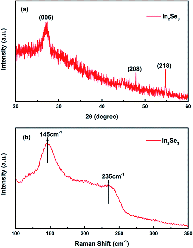 | ||
| Fig. 1 (a) The XRD pattern and (b) the Raman spectra of In2Se3 film. | ||
The typical current–voltage (I–V) characteristics of (Ag, Ta)/In2Se3/ITO cells with a current compliance of 100 mA are shown in Fig. 2, and the arrows indicate the sweeping directions (step 1 → step 2 → step 3 → step 4). It is obvious that the resistance of Ta/In2Se3/ITO device is much higher than that of the Ag/In2Se3/ITO device, which is due to the fact that Ag is an active electrode and Ta is an inert electrode. The Ag/In2Se3/ITO cell exhibits stable bipolar resistive switching behavior during the 100-cycle subsequent voltage sweeping process from 2.5 to −2.5 V, as shown in Fig. 2(a). The I–V characteristics of the devices is shifted from a high-resistance state (HRS) to a low-resistance state (LRS) by a positive bias sweep, known as the SET process. Then, they return to HRS by a negative bias sweep, known as the RESET process. As shown in Fig. 2(b), the threshold voltages for the Ag/In2Se3/ITO cell in the positive and negative regions are approximately 0.9 V (SET) and −1.0 V (RESET), respectively. However, the Ta/In2Se3/ITO cell has different I–V characteristics as shown in Fig. 2(c), which exhibits stable bipolar resistive switching behavior during the 100-cycle subsequent voltage sweeping process from 5 to −5 V. Fig. 2(d) reveals that the threshold voltages of the Ta/In2Se3/ITO cell in the positive and negative regions are approximately 1.5 V (SET) and −1.3 V (RESET), respectively. The relative larger SET/RESET values of Ta/In2Se3/ITO cell is attributed to Ta as an inert electrode instead of Ag, which causes a larger intensity injecting current. In addition, the resistance of Ta/In2Se3/ITO cell is continuous rather than an abrupt jump compared to that of Ag/In2Se3/ITO cell. From the macroscopic perspective, the two kinds of chosen electrodes have similar work functions. Because the Ag electrode is active and Ta electrode is inert one, the memristor with Ag top electrode has little resistance at the same bias voltage. Thus, the injection current in the memristor sample is greater than that with the Ta electrode. From the microscopic mechanism, the effect of the two different top electrodes is to effectively control the carrier mobility of the core layer through the applied bias electric field introduced by the electrodes. In the meantime, all of the In2Se3 core layer are crystalline after thermal treatment. Thus, there should be an interface layer between the silver top electrode and the In2Se3 core layer. This interface will have a certain impact on the I–V characteristics of the sample device.
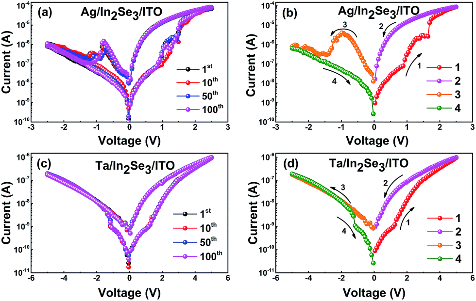 | ||
| Fig. 2 (a) The I–V characteristic of Ag/In2Se3/ITO in a certain times cycles test. (b) Typical bipolar I–V characteristic of Ag/In2Se3/ITO in sweeping DC voltages. (c) The I–V characteristic of Ta/In2Se3/ITO in a certain times cycles test. (d) Typical bipolar I–V characteristic of Ta/In2Se3/ITO in sweeping DC voltages. | ||
Several conduction mechanism models7,31 have been developed to describe the underlying mechanisms of the nonlinear I–V characteristics including Schottky emission, Poole–Frenkel emission (P–F), Fowler–Nordheim tunnelling (F–N), SCLC and so on. The method to distinguish these conduction mechanisms is essential because there are several available conduction mechanisms contributing to the device conduction current at the same time.
In order to discuss the conduction mechanism of Ag/In2Se3/ITO cell, the I–V curves have been replotted using log scale as shown in Fig. 3. The trap-controlled SCLC mechanism can well account for the conducting I–V features. As we know, three key factors, i.e. an ohmic regime, a trap-filled limited regime, and Child's square law region, constitute the trap-controlled SCLC. The current density for trap-controlled SCLC emission can be expressed as follows,35
 | (1) |
 | (2) |
 | ||
| Fig. 3 (a) The I–Vn curves of Ag/In2Se3/ITO in positive voltage region. (b) The I–Vn curves of Ag/In2Se3/ITO in negative voltage region. | ||
Generally, the defects in the polycrystalline chalcogenide can be divided into two types, (i) defects within the crystalline grain, (ii) defects at the grain boundaries arising from dangling bonds. These defects form localized states near the valance band, which can act as charge traps and absorb injected carriers. Therefore, the current can be described by20
 | (3) |
 | (4) |
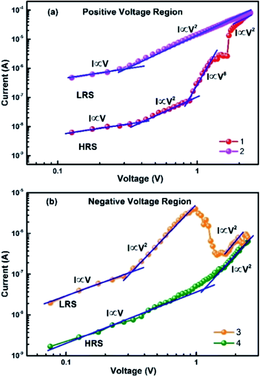
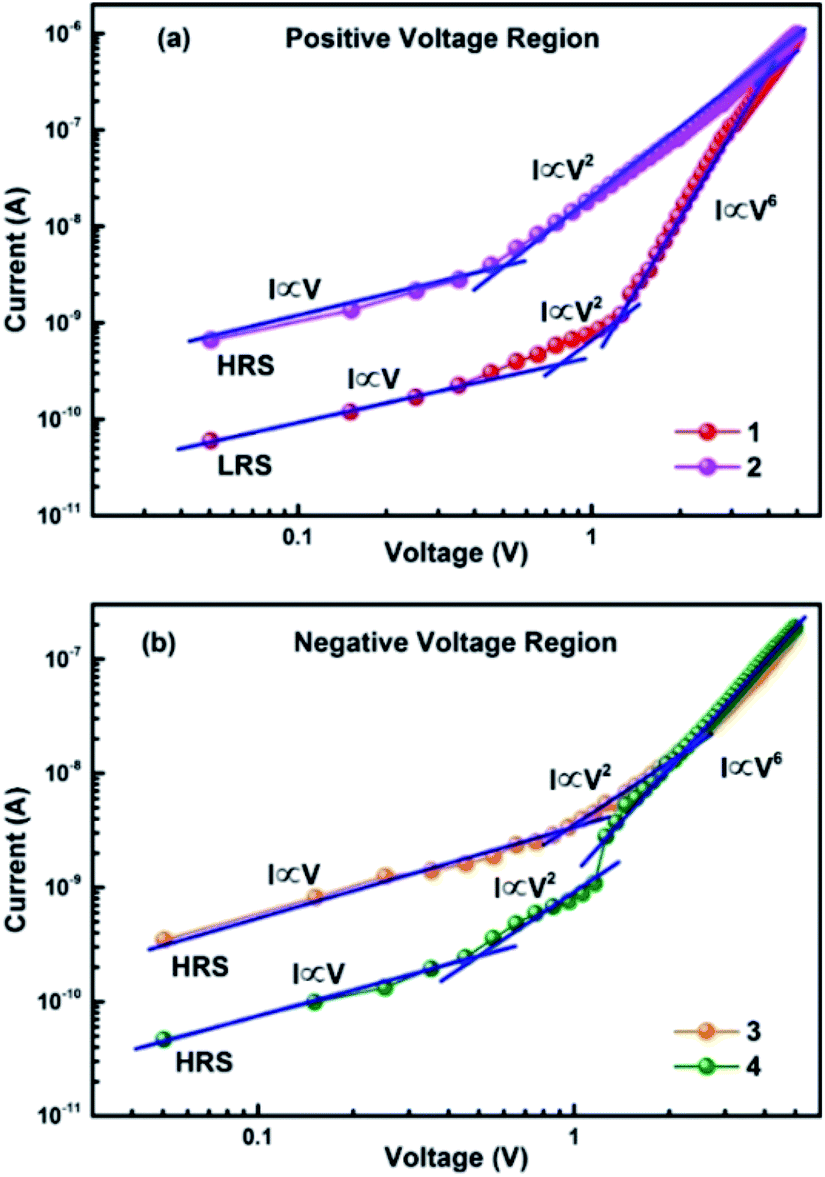
In the positive voltage region, as shown in Fig. 3(a), it is clear that the I–V characteristics is dominated by the linear ohmic law (I ∝ V) at low voltage because the density of thermally generated free carriers inside the cell is predominant over the injected charge carriers. When the applied voltage reaches 0.37 V, the I–V curve changes from the ohmic to trap-filled limited SCLC conduction. Initially, the SCLC is controlled by single shallow traps, and the current, given by eqn (1), has a square law dependence on voltage (I ∝ V2). When the bias increases well above the trap-filled limit voltage (VT ≈ 0.88 V), the rapid increase in current (I ∝ V8) indicates a transition from single shallow trap controlled SCLC to exponentially distributed trap controlled SCLC, and the I–V relationship is given by eqn (3). Finally, all the traps are filled and the current follows square dependence on voltage, corresponding to the Child's square law region (I ∝ V2). Thus, the process in the positive voltage region can be described as ohmic → SCLC conduction (controlled by single shallow trap) → SCLC (controlled by traps with exponential distribution) → Child's law → ohmic.
In the negative voltage region, as shown in Fig. 3(b), it is observed that the I–V characteristics in the 0 V → −2 V region is similar to that in the 2 V → 0 V region before the voltage reaches at  . When the sweep voltage is beyond
  , the current reduces with increasing voltage. The trapped carriers are released at
  and the conduction mode changes from the SCLC (controlled by traps with exponential distribution) to SCLC (controlled by single shallow trap). The slop of current controlled by traps with exponential distribution is changed abruptly, which is different from the positive region. The I–V characteristics transit from SCLC (controlled by single shallow trap) to ohmic conduction during the sweep voltage of −2 V → 0 V. Thus, the process in the negative voltage region can be described as ohmic → Child's law → SCLC conduction (controlled by traps with exponential distribution) → SCLC (controlled by single shallow trap) → ohmic.
In order to understand the top electrode effect, the I–V curves of the Ta/In2Se3/ITO cell have been replotted using log scale, as shown in Fig. 4. The result is similar to the behavior of the Ag/In2Se3/ITO cell. The conduction behavior obeys SCLC mechanism conduction. In the positive voltage region, the I–V curves shows linear behavior under low voltage and then quadratic. At the voltage (VT ≈ 1.16 V), the current rises rapidly and the slope reaches ∼6. Then the current rises slowly and the slope reduces to 2. In the negative voltage region, the trapped carriers are released at  and then the slope reaches ∼6. The current of Ta/In2Se3/ITO device is smaller due to the weaker injection, while the current of Ag/In2Se3/ITO is larger due to the stronger injection.
 | ||
| Fig. 4 (a) The I–Vn curves of Ta/In2Se3/ITO in positive voltage region. (b) TheI–Vn curves of Ta/In2Se3/ITO in negative voltage region. | ||
The resistance of Ta TE is tuneable continuously distinguishing with the Ag TE, which is related to the strong injecting current of the Ag TE than the Ta TE. The values of VT and  in the two cells are different since Ag is an active electrode and Ta is an inert electrode.
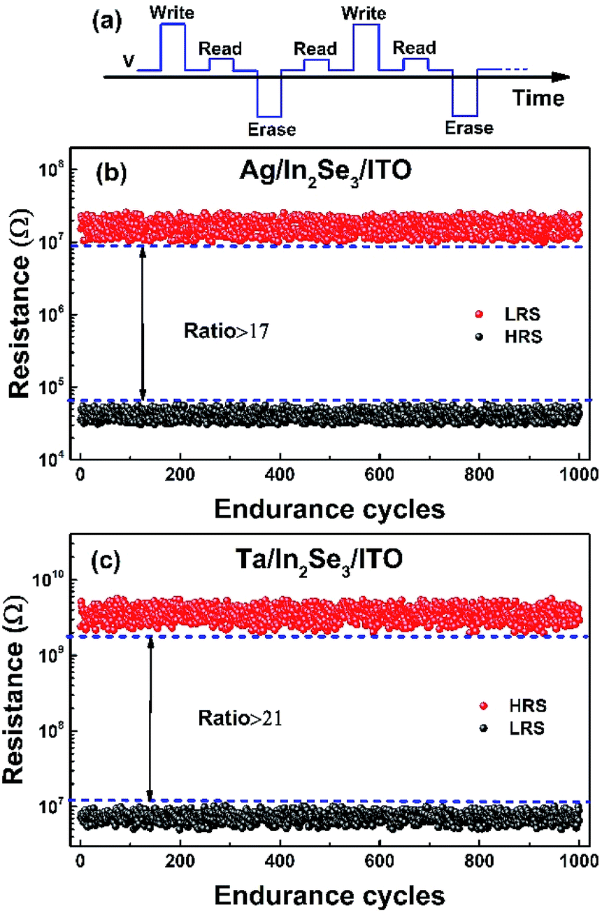
To further investigate the performances of the Ag/In2Se3/ITO and Ta/In2Se3/ITO devices, the cycling endurance characteristics were measured in the pulse sweep mode with 1000 cycles, respectively, as shown in Fig. 5. The applied plus is 2 V μs−1 for SET process and −2 V for the RESET process, respectively. The reading voltage is 0.5 V as shown in Fig. 5(a). Fig. 5(b) shows the endurance behavior of Ag/In2Se3/ITO cell in 1000 cycles test without sensing margin deterioration. It is obvious that the HRS is more discrete than the LRS due to the more stable LRS of the cell. The resistance ratio of HRS/LRS is at least 17 times large enough for the periphery circuits to probe the different resistance states. Fig. 5(c) shows the endurance behavior of Ta/In2Se3/ITO cell in 1000 cycles test without switching failure. It is obvious that the HRS is more discrete than the LRS due to the wide distribution HRS of the cell. The resistance ratio of HRS/LRS is more than 21 times large enough for distinguishing in storage application. The power consumption of the Ta TE is lower than that of Ag, which makes the Ta/In2Se3/ITO cell more suitable for storage application rather than the Ag/In2Se3/ITO device due to higher ratio of HRS/LRS and low power consumption. The similar results for the endurance cycle tests of these two kinds of cell can be attributed to the same resistance switching conduction mechanism.
 | ||
| Fig. 5 (a) The plus excitation voltage. (b) The resistance of Ag/In2Se3/ITO cell in 1000 cycles test. (c) The resistance of Ta/In2Se3/ITO cell in 1000 cycles test. | ||
Conclusions
In summary, based on the In2Te3 core layer, two kinds of Ag/In2Se3/ITO and Ta/In2Se3/ITO asymmetrical hetero-structures had been successfully prepared using magnetron sputtering method. Experimental characterizations including structure, spectra and electronic properties were investigated by XRD, Raman spectroscopy and semiconductor parameter analyser respectively. The main Raman peaks were identified as the γ-phase of In2Se3 structure which conformed by the XRD results. The two kinds of sandwich structure devices with In2Se3 core layer show bipolar memristive switching behavior and possess the properties of reversible switching, reproducible resistance, non-destructive readout, good cycling performance and nonvolatile. The intrinsic memristive characteristics conforms to the SCLC mechanism that is contributed by the defects existing in the polycrystalline chalcogenide of In2Se3 core layer. The Ag top electrode in the asymmetrical hetero-structure shows the lower interface resistance and strong injection that the resistance change is an abrupt jump suitable for storage application, while the Ta top electrode presents the higher interface resistance and weak injection that resistance change is continuous suitable for neuromorphic circuits application.Conflicts of interest
There are no conflicts to declare.Acknowledgements
The authors would like to express their sincere thanks for the financial supports by the funding under Grant No. 17ZR1402200, 13ZR1402600, 60578047, 61427815 and 2015KF003. The authors thank Prof. L. Y. Chen and Prof. M. Xu for effective backup.References
- L. O. Chua, IEEE Trans. Circuit Theory, 1971, 18, 507–512 CrossRef.
- B. Sun, Y. X. Liu, L. F. Liu, N. Xu, Y. Wang, X. Y. Liu, R. Q. Han and J. F. Kang, J. Appl. Phys., 2009, 105, 061630 CrossRef.
- F. M. Simanjuntak, D. Panda, K. H. Wei and T. Y. Tseng, Nanoscale Res. Lett., 2016, 11, 368 CrossRef PubMed.
- J. Borghetti, G. S. Snider, P. J. Kuekes, J. J. Yang, D. R. Stewart and R. S. Williams, Nature, 2010, 464, 873–876 CrossRef CAS PubMed.
- E. Linn, R. Rosezin, S. Tappertzhofen, U. Bottger and R. Waser, Nanotechnology, 2012, 23, 305205 CrossRef CAS PubMed.
- R. A. Nawrocki, R. M. Voyles and S. E. Shaheen, IEEE Trans. Electron Devices, 2016, 63, 3819–3829 CrossRef.
- T. Shi, X. B. Yin, R. Yang and X. Guo, Phys. Chem. Chem. Phys., 2016, 18, 9338–9343 RSC.
- Y. J. Noh, Y.-J. Baek, C. J. K. Q. Hu, Y. J. Choi, H. H. Lee and T.-S. Yoon, IEEE Trans. Nanotechnol., 2015, 14, 798–805 CrossRef CAS.
- J. X. Zha, H. Huang and Y. J. Liu, IEEE Trans. Circuits Syst., 2016, 63, 423–424 CrossRef.
- D. B. Strukov, G. S. Snider, D. R. Stewart and R. S. Williams, Nature, 2008, 453, 80–83 CrossRef CAS PubMed.
- J. J. Yang, M. D. Pickett, X. Li, D. A. Ohlberg, D. R. Stewart and R. S. Williams, Nat. Nanotechnol., 2008, 3, 429–433 CrossRef CAS PubMed.
- P. Zhou, J. Li, L. Y. Chen, T. Tang and Y. Lin, Chin. Phys. Lett., 2008, 25, 3742–3744 CrossRef CAS.
- W. Kim, S. Menzel, D. J. Wouters, Y. Guo, J. Robertson, B. Roesgen, R. Waser and V. Rana, Nanoscale, 2016, 8, 17774–17781 RSC.
- D. Panda, C.-Y. Huang and T.-Y. Tseng, Appl. Phys. Lett., 2012, 100, 112901 CrossRef.
- D. Panda and T.-Y. Tseng, Thin Solid Films, 2013, 531, 1–20 CrossRef CAS.
- F. M. Simanjuntak, D. Panda, T.-L. Tsai, C.-A. Lin, K.-H. Wei and T.-Y. Tseng, Appl. Phys. Lett., 2015, 107, 033505 CrossRef.
- F. M. Simanjuntak, O. K. Prasad, D. Panda, C. A. Lin, T. L. Tsai, K. H. Wei and T. Y. Tseng, Appl. Phys. Lett., 2016, 108, 183506 CrossRef.
- R. Muenstermann, T. Menke, R. Dittmann and R. Waser, Adv. Mater., 2010, 22, 4819–4822 CrossRef CAS PubMed.
- S. Stille, C. Lenser, R. Dittmann, A. Koehl, I. Krug, R. Muenstermann, J. Perlich, C. M. Schneider, U. Klemradt and R. Waser, Appl. Phys. Lett., 2012, 100, 223503 CrossRef.
- Y. Li, Y. P. Zhong, J. J. Zhang, X. H. Xu, Q. Wang, L. Xu, H. J. Sun and X. S. Miao, Appl. Phys. Lett., 2013, 103, 043501 CrossRef.
- J. J. Zhang, N. Liu, H. J. Sun, P. Yan, Y. Li, S. J. Zhong, S. Xie, R. J. Li and X. S. Miao, J. Electron. Mater., 2015, 45, 1154–1159 CrossRef.
- S. J. Wei, H. F. Zhu, K. Chen, D. Xu, J. Li, F. X. Gan, X. Zhang, Y. J. Xia and G. H. Li, Appl. Phys. Lett., 2011, 98, 231910 CrossRef.
- A. Gubicza, D. Z. Manrique, L. Posa, C. J. Lambert, G. Mihaly, M. Csontos and A. Halbritter, Sci. Rep., 2016, 6, 30775 CrossRef CAS PubMed.
- T. W. Kim, H. Choi, S. H. Oh, M. Jo, G. Wang, B. Cho, D. Y. Kim, H. Hwang and T. Lee, Nanotechnology, 2009, 20, 025201 CrossRef PubMed.
- L. Li and D. Wen, Org. Electron., 2016, 34, 12–17 CrossRef CAS.
- M. Fujimoto, H. Koyama, Y. Nishi and T. Suzuki, Appl. Phys. Lett., 2007, 91, 223504 CrossRef.
- A. Chanthbouala, V. Garcia, R. O. Cherifi, K. Bouzehouane, S. Fusil, X. Moya, S. Xavier, H. Yamada, C. Deranlot, N. D. Mathur, M. Bibes, A. Barthelemy and J. Grollier, Nat. Mater., 2012, 11, 860–864 CrossRef CAS PubMed.
- D. Panda and T. Y. Tseng, Ferroelectrics, 2014, 471, 23–64 CrossRef CAS.
- N. T. Ho, V. Senthilkumar and Y. S. Kim, Solid-State Electron., 2014, 94, 61–65 CrossRef CAS.
- M. Rogala, P. J. Kowalczyk, P. Dabrowski, I. Wlasny, W. Kozlowski, A. Busiakiewicz, S. Pawlowski, G. Dobinski, M. Smolny, I. Karaduman, L. Lipinska, R. Kozinski, K. Librant, J. Jagiello, K. Grodecki, J. M. Baranowski, K. Szot and Z. Klusek, Appl. Phys. Lett., 2015, 106, 263104 CrossRef.
- M. Park, S. Park and K. H. Yoo, ACS Appl. Mater. Interfaces, 2016, 8, 14046–14052 CAS.
- F. C. Chiu, Adv. Mater. Sci. Eng., 2014, 2014, 1–18 Search PubMed.
- A. A. A. Darwish, M. M. El-Nahass and M. H. Bahlol, Appl. Surf. Sci., 2013, 276, 210–216 CrossRef CAS.
- A. F. Qasrawi, J. Electron. Mater., 2013, 42, 1033–1036 CrossRef CAS.
- Q. Liu, W. Guan, S. Long, R. Jia, M. Liu and J. Chen, Appl. Phys. Lett., 2008, 92, 012117 CrossRef.
| This journal is © The Royal Society of Chemistry 2017 |