
 Open Access Article
 This Open Access Article is licensed under a
 Creative Commons Attribution 3.0 Unported Licence
Ultra-narrow terahertz perfect light absorber based on surface lattice resonance of a sandwich resonator for sensing applications
Ben-Xin Wang *a,
Wei-Qing Huang*b and
Ling-Ling Wangb
*a,
Wei-Qing Huang*b and
Ling-Ling Wangb
aSchool of Science, Jiangnan University, Wuxi, 214122, China. E-mail: wangbenxin@hnu.edu.cn
bSchool of Physics and Electronics, Hunan University, Changsha, 410082, China. E-mail: wqhuang@hnu.edu.cn
First published on 5th September 2017
Abstract
Perfect light absorbers have attracted much attention because of their potential applications in solar cells, thermal imaging, material detection, bio-sensing, and others. However, it is extremely difficult to obtain the ultra-narrow bandwidth of a perfect light absorber in the terahertz region. Herein, an ultra-narrow terahertz perfect light absorber based on the surface lattice resonance of three stacking layers, namely a square resonator, a dielectric spacer, and a metallic film, is reported. A resonance absorption peak with bandwidth of 0.0200 THz and absorption rate of 98.86% is realized. The absorption performance of the device can be controlled by employing different sized (unit) periods and dielectric spacer thicknesses. Particularly, the device bandwidth can be decreased by reducing the dielectric layer thickness. At a certain thickness, a resonance peak with a bandwidth of only 0.0067 THz is achieved. This peak is very sensitive to the surrounding refractive index. The large sensitivity (2.58 THz per refractive index) and simultaneous ultra-narrow bandwidth lead to an ultra-high figure of merit (385.07), making this a promising light device in terahertz detection and sensing.
Introduction
Metamaterials with sub-wavelength-scale metallic patterns can have many novel electromagnetic properties, from negative refractive indices1 to perfect lensing2 and invisible cloaking,3 that cannot be directly obtained in nature. Metamaterials can also enable novel or enhanced functions in many kinds of devices, such as switches,4 filters,5 modulators,6 sensors,7 and others.8–10 These function devices are mainly attributed to the unique properties of the metallic patterns that support surface propagation mode and localized resonance response. An important issue in the application of these devices is that metallic-based metamaterial structures inevitably have inherent (or dissipation) losses,11–13 which can limit their application abilities.However, it has recently been shown that the inherent losses in metallic structures can be used to enhance light absorption and achieve unity (or perfect) absorption via specific structures. A resonance device that can achieve perfect absorption of incident waves is usually called a perfect metamaterial absorber (PMA). The first PMA operating at microwave frequency was demonstrated in 2008 by utilizing a sandwich structure consisted of an electric-ring metallic resonator, an insulation dielectric layer, and a metallic strip.14 In addition to a near-perfect absorption peak in the sandwich structure, its dielectric layer thickness was much smaller (only 1/35) than the absorption wavelength. Compared with traditional Salisbury and Jaumann absorbers,15,16 the ultra-thin dielectric layer thickness makes the PMA lightweight and easy to fabricate. Therefore, many PMAs with different sizes and shapes of metallic patterns have been reported.17–40
According to differences in the resonance bandwidth, these PMAs are usually divided into narrowband PMAs17–32 and broadband PMAs.33–40 Broadband PMAs can be used in solar cells and stealth technology. Narrowband PMAs are generally used in areas such as selective thermal emitters, thermal imaging, material detection, and sensing. However, the bandwidths of narrowband PMAs are typically larger than 10% of the central resonance frequency. If converted to quality factor (Q, the ratio of resonance frequency to bandwidth), the Q values of the narrow-band PMAs do not usually exceed 10. The Q value is an important index of sensing performance. Therefore, to enhance the sensing sensitivities of PMAs, large Q values are required.
Different physical mechanisms have been employed to achieve large Q values for PMAs to improve their sensing sensitivity.41–50 For example, a large Q value of 120 was achieved by employing four silver disks (in the frequency range 800–1000 nm) in a super-unit cell;41 Li et al. achieved a Q value of 80 in the frequency range 600–900 nm using nanoscale metallic surfaces.42 He et al.43 obtained a Q value of about 100 in the frequency range 600–900 nm using a solid-inverse compound metamaterial. Unfortunately, investigations into PMAs with high Q values have mainly been focused on short wavelengths, such as optical and near-infrared regions. There have been only few reports of metamaterial resonators with high Q values at longer wavelengths, such as terahertz region.51,52
Herein, an ultra-narrow terahertz perfect light absorber is presented, which can be used to analyze tiny changes in the refractive index of its surroundings. This device contained three functional layers, namely a metallic layer with a patterned square ring placed on two stacking layers of insulation dielectric layer and metallic film. A narrow-band resonance absorption peak with a bandwidth of 0.0200 THz and absorption rate of 98.86% was obtained. Results showed that the values of Q and figure of merit (FOM) could reach 144.06 and 118.31, respectively. The underlying mechanism of narrowband absorption is attributed to surface lattice resonance (SLR) of the device, which is completely different from previous metamaterial-based light absorbers with three stacking layers that utilized magnetic resonance or interference theory mechanisms.
We further demonstrate that the absorption performance of the device can be controlled by employing different period (unit) sizes and dielectric layer thicknesses. As a special case, an ultra-narrow absorption peak with bandwidth of only 0.0067 THz is achieved, with a Q value of 442.18. The ultra-narrow absorption peak is highly sensitive to the refractive index of the surroundings. The sensing sensitivity and FOM of the device can be up to 2.58 THz per refractive index and 385.07, respectively. The Q values and FOM of the presented perfect light absorber are much larger than those previously reported metamaterial-based terahertz function devices, as shown in Table 1.
Results and discussion
A schematic of the ultra-narrow perfect light absorber is shown in Fig. 1(a) and (b), which is arranged periodically in the x- and y-axis directions. The device consisted of a sandwich-structured square Au ring, dielectric spacer, and opaque Au film. The Au ring had a length (l) of 70 μm, width (w) of 5 μm, thickness of 0.4 μm, and conductivity (σ) of 4.09 × 10⁷ S m−1. The dielectric spacer had a thickness (t) of 6.5 μm and dielectric constant of 3(1 + i0.06). The (unit) period of the device was Px = Py = P = 100 μm. The Au film was thick enough to block the transmission of incident plane waves. Furthermore, the sandwich structure should be placed on a solid substrate, such as silica or silicon, and the refractive index of surrounding was set to n = 1 (vacuum or air).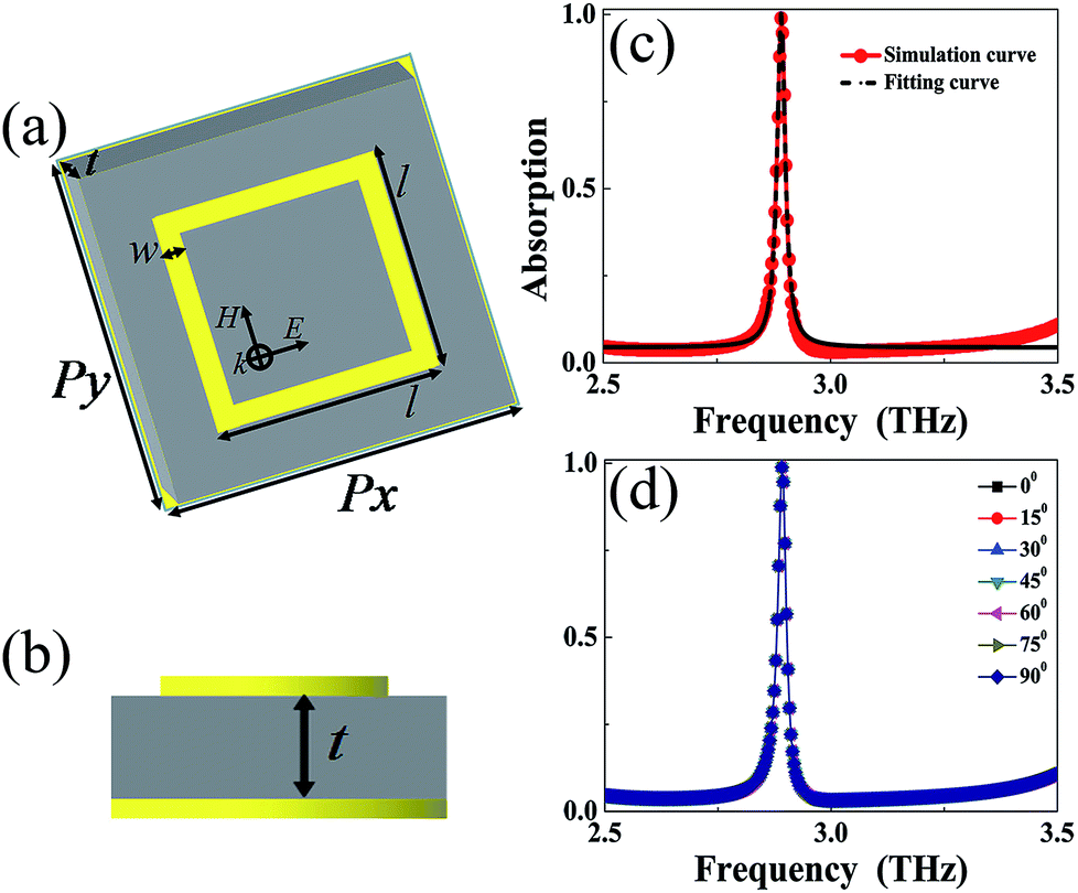 | ||
| Fig. 1 (a) Schematic diagram of the three-dimensional unit cell of the ultra-narrow perfect light absorber. (b) Side-view of the structure in (a). (c) Absorption spectra of the ultra-narrow perfect light absorber, of which the red and black curves are the simulation and fitting results, respectively. (d) Dependence of the simulated absorption spectra on different polarization angles of the perfect light absorber. | ||
The absorption responses and field distributions of the ultra-narrow perfect light absorber were determined using commercially available simulation software FDTD solutions, which is based upon the algorithm of the finite-difference time domain. The three-dimensional unit cell shown in Fig. 1(a) is periodically distributed in the x and y directions, and so periodic boundary conditions were used in these two directions. Light scattering was eliminated by employing perfectly matching layers in the z direction. A plane electromagnetic wave along the z-axis with an electric field parallel to the x-axis was irradiated into the designed unit cell. The absorption rate (AT) of the ultra-narrow perfect light absorber was calculated using AT = 1 − T − R, where T and R are the transmission and reflection of the device, respectively. As opaque Au film was present in the bottom layer of the device, transmission T could be prevented, allowing AT to be expressed as 1 − R. Reflection R can be suppressed by optimizing the impedance of the device.
The red curve in Fig. 1(c) presents the simulation absorption spectra of the designed terahertz perfect light absorber. An obvious resonance absorption peak was obtained at a frequency of 2.8913 THz with an absorption rate of 98.86%. Notably, as most studies have, we defined FWHM (full-width at half-maximum) as the resonance bandwidth of the device. Using this definition, its bandwidth was about 0.0200 THz, which is only 0.6917% of the central resonance frequency. This converted into a quality factor, Q, of 144.5650. Furthermore, the absorption performance of the perfect light absorber was polarization insensitive to the incident waves because of the high degree of symmetry of the square Au ring, as shown in Fig. 1(d).
For optical, infrared, and even terahertz frequency regions, when metallic patterned resonators, such as Au nanorods, Au nanodisks, and rectangular antenna arrays, are placed in a wavelength-scale array, a sharp resonance mode, due to SLR, can be obtained.42,54–63,72 SLR is essentially the complex combination effect of dipole resonances in individual metallic patterns and the diffraction (in particular, first-order diffraction) of metallic patterns, with the diffraction mode playing a major (or decisive) role in determining the resonance frequency of the sharp resonance mode.42 For more detailed theoretical analysis, please refer to ref. 54 and 55. Herein, we found that the resonance wavelength of the ultra-narrow absorber device was about 103.76 μm (at 2.8913 THz), which was very close to the unit period (100 μm) or wavelength scale of the resonator. Therefore, we believe that the physical mechanism of the narrow-band terahertz resonance device can be attributed to SLR, which is completely different from previous metamaterial-based light absorbers with sandwich structure models that utilize magnetic resonance or interference theory mechanisms. Therefore, we employed the concept of SLR to explain the physical mechanism and analyze the performance of this narrow-band terahertz perfect light absorber.
As SLR involves interplay of the dipole resonance of the individual metallic resonator and the first-order diffraction mode, the resonance frequency (or wavelength) of the SLR in simulation results should be slightly smaller (or larger) than the theoretical value of the first-order diffraction mode.54–60 In a pattern metallic array, diffraction can result in a strong resonance (SLR) when the grating order is changed from evanescent to radiative.54–56,60,64 The resonance wavelength of the SLR can be given by:54–56,72
 | (1) |
 | (2) |
To better understand the mechanism of narrow-band absorption, the effect of device parameter changes was investigated. Simulation absorption spectra and fitting results of the designed device with changes in the unit period P (or grating constant) are illustrated in the solid and dot curves of Fig. 2(a), respectively. The simulation results were in good agreement with the fitting results. In particular, we found that the resonance frequency of the large light absorption device was intensely affected by the period P (or the grating constant).42 However, other parameter changes, such as the length l and width w of the Au square ring, of the resonator had a slight influence on the resonance frequency of the ultra-narrow absorption device, as shown in Fig. 2(c) and (d). These results indicated that the period P (or grating constant) was the most important factor (or parameter) in determining the resonance frequency of the absorption device, while changes in the length l and width w of the Au square ring only afforded minor modifications in the resonance frequency.42,54–63 The physical mechanism of ultra-narrow absorption device was identified as SLR because the periodic effect usually offers a markedly narrow line-shape depending on the lattice constant P.42,54–63
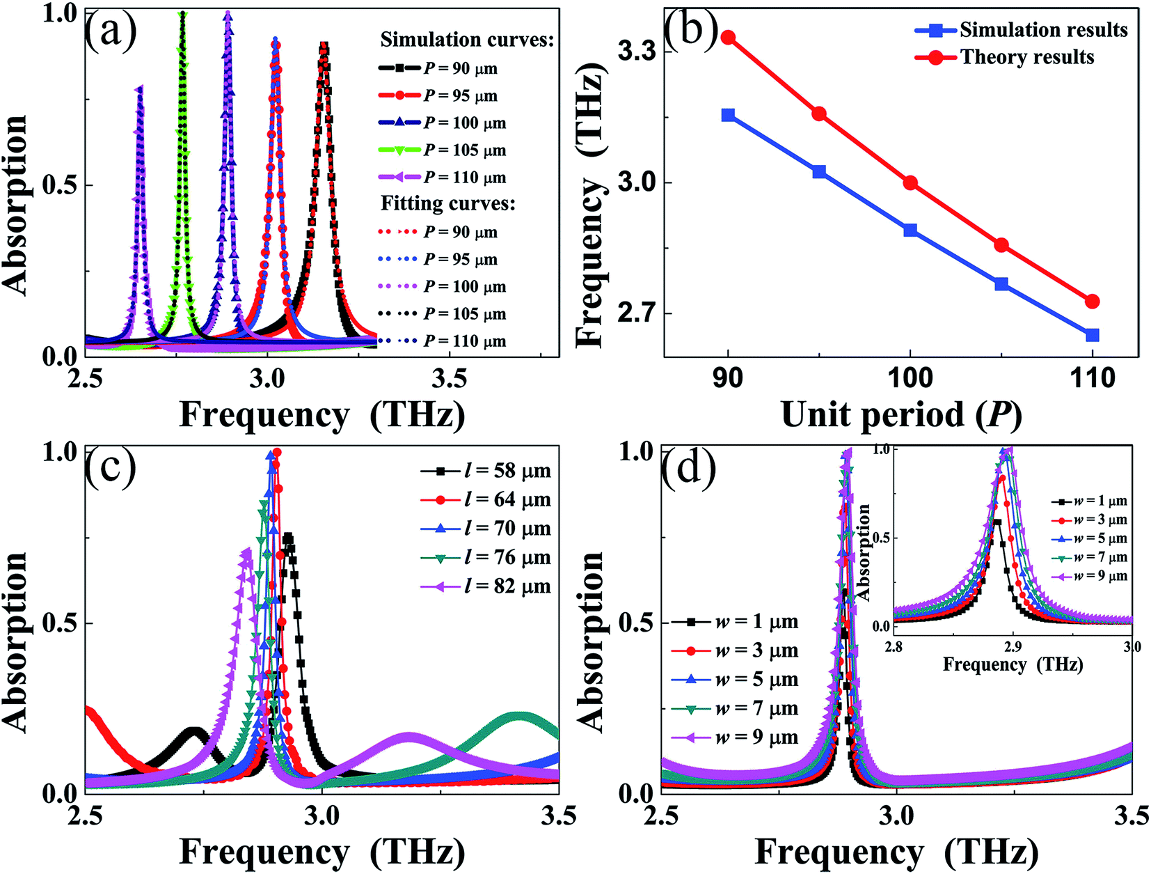 | ||
| Fig. 2 (a) Dependence of absorption spectra on changes in the period P (or grating constant) of the ultra-narrow perfect light absorber; solid and dot curves are the simulation and fitting results, respectively. (b) Function relationship of the resonance frequency and period P (or grating constant). (c and d) Dependence of absorption spectra on changes in the length l and width w of the Au ring resonator, respectively. | ||
The functional relationship between the simulated resonance frequency and the period P (or grating constant) is shown by the blue line in Fig. 2(b). Changes in the simulated resonance frequency and period P showed an approximately linear inverse relationship, which was similar to the change trend in the theoretical results (red line in Fig. 2(b)). In particular, we observed that the resonance frequencies of the simulation results with any given period P (or grating constant) were all slightly smaller than the corresponding theoretical values, which was consistent with results in previous works.54–60 FD is defined as the frequency difference between the results of theory and simulation in any given period P (or grating constant). The FD was 0.1781 THz at P = 90 μm, 0.1328 THz at P = 95 μm, 0.1087 THz at P = 95 μm, 0.0895 THz at P = 105 μm, and 0.0768 THz at P = 110 μm. These results showed that the FD value gradually decreased with increasing period P (or grating constant). This trend further indicated that the frequency of the simulated absorption peak became closer to the theoretical value of the first-order diffraction mode (or SLR) when the period P was increased, in agreement with previous reports.54–60 The tuning of FD with the change in period P was new evidence demonstrating the resonance mechanism of the ultra-narrow absorption device. Furthermore, the electric field (|E|) distribution of the resonance absorption peak provides additional evidence for the resonance mechanism. As shown in Fig. 3(a), the electric field (on the plane that intersects the middle height of the Au square ring array) shows a delocalized distribution feature, with the field intensity enhanced almost throughout unit cell, which is totally different from previous metamaterial-based absorbers, in which the electric fields were mainly focused on the edges of the metallic arrays and only supported the dipole resonance characteristics. We also found that the field distributions of a group of four Au square rings demonstrated delocalized distribution features, as shown in Fig. 3(b). These field distributions offer additional evidence to support SLR as the mechanism of this ultra-narrow perfect light absorber.42,62,63
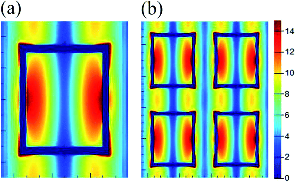 | ||
| Fig. 3 (a and b) Electric field distributions (on the plane that intersects the middle height of the Au ring array) of the single ring resonator and group of four rings, respectively, at a resonance frequency of 2.8913 THz (P = 100 μm). | ||
The absorption performance of the narrow-band device could be controlled by changing its dielectric thickness t. The absorption dependence on the thickness t of the device is shown in Fig. 4(a). Unlike the change in period P, changing thickness t not only affected the resonance frequency, but also the absorption rate. Firstly, regarding the effect on resonance frequency, the absorption frequency of the device gradually decreased with increasing thickness t. This kind of absorption feature was similar to the changing trend of period P. However, the frequency change range of the device was be up to 0.03177 THz per micron for thickness t, which was larger than that of the period P (0.02524 THz per micron). Secondly, regarding the influence on absorption rate, the change in the absorption rate showed two trends: (1) a rapid increase when the thickness t was increased from t = 3.5 μm to the optimum thickness of t = 6.5 μm, and (2) a slight increase when the thickness t was further increased. These trends were different from the case of period P in Fig. 2(a).
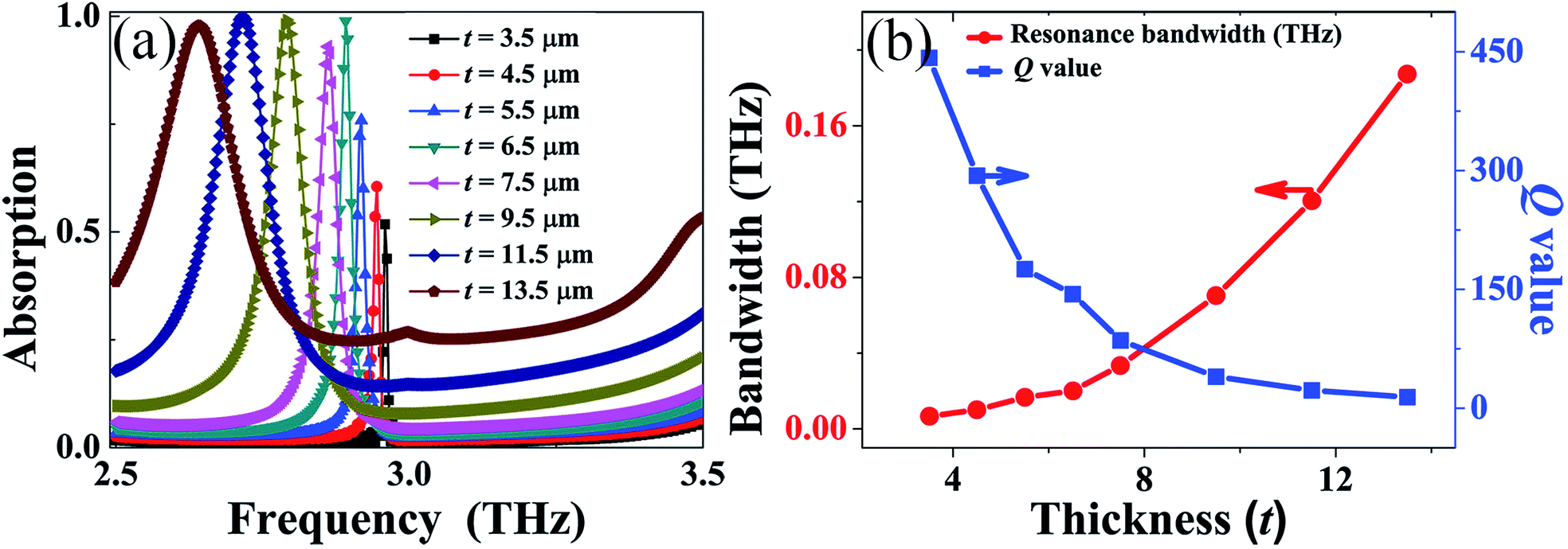 | ||
| Fig. 4 (a) Dependence of absorption spectra on changes in the dielectric thickness t of the ultra-narrow perfect light absorber. (b) Dependence of the resonance bandwidth and Q value on changes in the dielectric spacer thickness t. | ||
In addition to frequency shift and absorption rate changes, the bandwidth of the device showed obvious variation. The red line in Fig. 4(b) shows the changing trend. As shown, the bandwidth of the device rapidly increased from 0.0067 THz at t = 3.5 μm to 0.1873 THz at t = 13.5 μm. Due to the rapid broadening of the resonance bandwidth, the corresponding Q value of the device should decrease rapidly. As shown by the blue line in Fig. 4(b), the Q value sharply decreased with increasing thickness t. In particular, the Q value of thickness t = 3.5 μm (441.52) was about 31.32 times larger than that at t = 13.5 μm (14.10). The ultra-narrow and ultra-high Q value of the terahertz perfect light absorber could find numerous applications in sensing-related fields. The next section details the effect of slight changes in the refractive index of the surrounding on the sensing performance of the device.
Sensing performance analysis
The absorption frequency of the narrow-band perfect light absorber is highly reliant on the refractive index of the surroundings. This effect can usually be employed to design different types of sensor. The sensing capability of the sensor is typically described using the sensing sensitivity (S). The definition of sensitivity, S, is:| S = Δf/Δn | (3) |
| FOM = S/FWHM | (4) |
We investigated the sensing capabilities of two groups of ultra-narrow perfect light absorber under different dielectric spacer thicknesses. We firstly analyzed the sensing performance of optimal absorption of the narrow-band device at thickness t = 6.5 μm, and its absorption is shown in Fig. 1(c). To investigate sensing performance, the refractive index of the surrounding (above the Au square resonator) can be changed from air (n = 1.00) to 1.10 with an interval of 0.02, with the corresponding absorption curves shown in Fig. 5(a). The resonance frequency of the narrow-band perfect light absorber gradually blue-shifted from the initial frequency at n = 1.00 when the refractive index of the surrounding was increased. The dependence of the frequency points on refractive index changes of the surrounding is illustrated in Fig. 5(b). The changes in frequency points and refractive indexes had an approximately linear inverse relationship. The slope shown in Fig. 5(b) should be the sensing sensitivity S, with a value of 2.37 THz per refractive index. Combined with the ultra-narrow bandwidth of 0.0200 THz, the FOM of the terahertz perfect light absorber at thickness t = 6.5 μm reached 118.50.
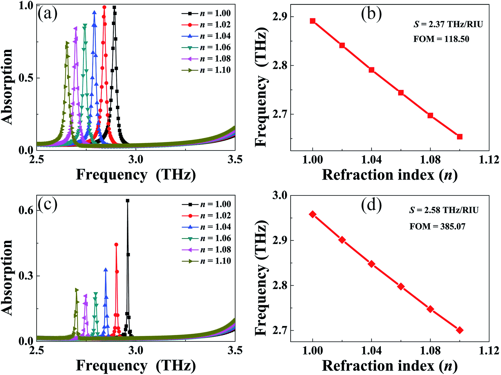 | ||
| Fig. 5 (a and c) Dependence of absorption spectra on changes in refractive indexes at different thicknesses of t = 6.5 μm and t = 3.5 μm, respectively. (b and d) Function relationship of resonance frequency and refractive index at different thicknesses of t = 6.5 μm and t = 3.5 μm, respectively. | ||
We next investigated the sensing capability of the ultra-narrow perfect light absorber at thickness t = 3.5 μm. The resonance bandwidth was only 0.0067 THz, which was smaller than (about 1/3) that at t = 6.5 μm. The dependence of the absorption on the refractive index of the surrounding is shown in Fig. 5(c). We observed that the device frequency gradually decreased with increasing of refractive index. In particular, the resonance frequency and corresponding refractive index approximately satisfied the linear inverse proportion relationship, as shown in Fig. 5(d). This kind of resonance feature was consistent with the case of t = 6.5 μm, as shown in Fig. 5(b). The sensitivity S (i.e., slope) of the ultra-narrow perfect light absorber at t = 3.5 μm was about 2.58 THz per refractive index, which was only slightly larger than that at t = 6.5 μm (2.37 THz per refractive index). The FOM was up to 385.07 at t = 3.5 μm, which was much higher than that at t = 6.5 μm (118.50). The ultra-high FOM was about two orders of magnitude larger than the microfluidic-based terahertz PMA,53 and was also much larger than previous terahertz-based light devices, as shown in Table 1.
Conclusions
In conclusion, an ultra-narrow terahertz perfect light absorber consisting of three layers, namely a square Au ring, insulation dielectric layer, and opaque Au film, is presented. The device can achieve near-perfect absorption of 98.86% and a bandwidth of 0.0200 THz, which is only 0.6917% of the central resonance frequency. Unlike previous metamaterial-based perfect light absorbers, which employed magnetic resonance or interference theory mechanisms, the underlying mechanism of the ultra-narrow absorber was surface lattice resonance. The device frequency can be effectively controlled using the period and thickness of the dielectric spacer layer. As a special example, at a dielectric thickness of 3.5 μm, the bandwidth decreased rapidly to only 0.0067 THz. The ultra-narrow bandwidth was only 0.0023% of the central resonance frequency, which was far smaller than that of widely studied metamaterial-based absorbers (about 10%). We further demonstrated that the ultra-narrow bandwidth of the device was extremely sensitive to the refractive index of the surrounding. The sensing sensitivity S and FOM of the ultra-narrow device were as high as 2.58 THz per refractive index and 385.07, respectively, which are much better than those of most reported at terahertz frequency, as shown in Table 1. The large sensing capability (in particular, FOM) of the terahertz perfect light absorber could find applications in terahertz detection, imaging and sensing.Conflicts of interest
The authors declare no competing financial interests.Acknowledgements
This work was supported by the National Natural Science Foundation of China (Grant No. 11647143), Natural Science Foundation of Jiangsu Province (Grant No. BK20160189), and the Fundamental Research Funds for the Central Universities (Grant No. JUSRP115A13).References
- N. Kaina, F. Lemoult, M. Fink and G. Lerosey, Nature, 2015, 525, 77 CrossRef CAS PubMed.
- G. Rosenblatt and M. Orenstein, Phys. Rev. Lett., 2015, 115, 195504 CrossRef PubMed.
- X. Ni, Z. J. Wong, M. Mrejen, Y. Wang and X. Zhang, Science, 2015, 349, 1310 CrossRef CAS PubMed.
- J. Y. Ou, E. Plum, J. Zhang and N. I. Zheludev, Nat. Nanotechnol., 2013, 8, 252 CrossRef CAS PubMed.
- W. Fu, Y. Han, J. Li, H. Wang, H. Li, K. Han, X. Shen and T. Cui, J. Phys. D: Appl. Phys., 2016, 49, 285110 CrossRef.
- C. M. Watts, D. Shrekenhamer, J. Montoya, G. Lipworth, J. Hunt, T. Sleasman, S. Krishna, D. R. Smith and W. J. Padilla, Nat. Photonics, 2014, 8, 605 CrossRef CAS.
- J. Grant, I. Escorcia-Carranza, C. Li, I. J. H. McCrindle, J. Gough and D. R. S. Cumming, Laser Photonics Rev., 2013, 7, 1043 CrossRef CAS.
- J. Gu, R. Singh, X. Liu, X. Zhang, Y. Ma, S. Zhang, S. A. Maier, Z. Tian, A. K. Azad, H. T. Chen, A. J. Taylor, J. Han and W. Zhang, Nat. Commun., 2012, 3, 1151 CrossRef PubMed.
- M. Amin, M. Farhat and H. Bagci, Sci. Rep., 2013, 3, 2105 CrossRef CAS PubMed.
- Z. Bai and G. Huang, Phys. Rev. A, 2016, 93, 013818 CrossRef.
- S. Wuestner, A. Pusch, K. L. Tsakmakidis, J. M. Hamm and O. Hess, Phys. Rev. Lett., 2010, 105, 127401 CrossRef PubMed.
- A. Fang, T. Koschny, M. Wegener and C. M. Soukoulis, Phys. Rev. B: Condens. Matter Mater. Phys., 2009, 79, 241104 CrossRef.
- O. Hess and K. L. Tsakmakidis, Science, 2013, 339, 654 CrossRef CAS PubMed.
- N. I. Landy, S. Sajuyigbe, J. J. Mock, D. R. Smith and W. J. Padilla, Phys. Rev. Lett., 2008, 100, 207402 CrossRef CAS PubMed.
- B. A. Munk, Frequency Selective Surfaces, John Wiley&Sons, New York, 2000 Search PubMed.
- W. W. Salisbury, US Pat., 2599944, 1952.
- K. Chen, T. D. Dao, S. Ishii, M. Aono and T. Nagao, Adv. Funct. Mater., 2015, 25, 6637 CrossRef CAS.
- P. T. Bowen, A. Baron and D. R. Smith, Phys. Rev. A, 2016, 93, 063849 CrossRef.
- G. M. Akselrod, J. Huang, T. B. Hoang, P. T. Bowen, L. Su, D. R. Smith and M. H. Mikkesen, Adv. Mater., 2015, 27, 8028–8034 CrossRef CAS PubMed.
- X. Zhao, J. Zhang, K. Fan, G. Duan, G. D. Metcalfe, M. Wraback, X. Zhang and R. D. Averitt, Photonics Res., 2016, 4, A16 CrossRef CAS.
- B. X. Wang and G. Z. Wang, Plasmonics, 2016, 11, 523 CrossRef CAS.
- Z. Li, S. Butun and K. Aydin, ACS Photonics, 2015, 2, 183 CrossRef CAS.
- B. X. Wang, X. Zhai, G. Z. Wang, W. Q. Huang and L. L. Wang, Opt. Mater. Express, 2015, 5, 227 CrossRef.
- G. Z. Wang and B. X. Wang, J. Lightwave Technol., 2015, 33, 5151 CrossRef.
- S. Qgawa, D. Fujisawa, H. Hata, M. Uetsuki, K. Misaki and M. Kimata, Appl. Phys. Lett., 2015, 106, 041105 CrossRef.
- W. C. Chen, A. Cardin, M. Koirala, X. Liu, T. Tyler, K. G. West, C. M. Bingham, T. Starr, A. F. Starr, N. M. Jokerst and W. J. Padilla, Opt. Express, 2016, 24, 6783 CrossRef CAS PubMed.
- M. P. Hokmabadi, D. S. Wilbert, P. Kung and S. M. Kim, Phys. Rev. Appl., 2014, 1, 044003 CrossRef.
- B. X. Wang, G. Z. Wang, L. L. Wang and X. Zhai, IEEE Photonics Technol. Lett., 2016, 28, 307 CrossRef.
- J. H. Kim, M. P. Hokmabadi, S. Balci, E. Rivera, S. Wilbert, P. Kung and S. M. Kim, Appl. Phys. A, 2016, 122, 362 CrossRef.
- N. Liu, M. Mesch, T. Weiss, M. Hentschel and H. Giessen, Nano Lett., 2010, 10, 2342 CrossRef CAS PubMed.
- B. X. Wang, X. Zhai, G. Z. Wang, W. Q. Huang and L. L. Wang, J. Appl. Phys., 2015, 117, 014504 CrossRef.
- J. Hao, J. Wang, X. Liu, W. J. Padilla, L. Zhou and M. Qiu, Appl. Phys. Lett., 2010, 96, 251104 CrossRef.
- Y. J. Kim, Y. J. Yoo, K. W. Kim, J. Y. Rhee, Y. H. Kim and Y. P. Lee, Opt. Express, 2015, 23, 3861 CrossRef CAS PubMed.
- W. Jiang, Y. Ma, J. Yuan, G. Yin, W. Wu and S. He, Laser Photonics Rev., 2016, 10, 1600253 Search PubMed.
- C. Gong, M. Zhan, J. Yang, Z. Wang, H. Liu, Y. Zhao and W. Liu, Sci. Rep., 2016, 6, 32466 CrossRef CAS PubMed.
- X. Zhang, Y. Fan, L. Qi and H. Li, Opt. Mater. Express, 2016, 6, 2448 CrossRef.
- Y. K. Zhong, Y. C. Lai, M. H. Tu, B. R. Chen, S. M. Fu, P. Yu and A. Lin, Opt. Express, 2016, 24, A832 CrossRef CAS PubMed.
- X. Huang, X. He, L. Guo, Y. Yi, B. Xiao and H. Yang, J. Opt., 2015, 17, 055101 CrossRef.
- H. Zhu, F. Yi and E. Cubukcu, Nat. Photonics, 2016, 10, 709 CrossRef CAS.
- S. Liu, H. Chen and T. J. Cui, Appl. Phys. Lett., 2015, 106, 151601 CrossRef.
- Z. Yong, S. Zhang, C. Gong and S. He, Sci. Rep., 2016, 6, 24063 CrossRef CAS PubMed.
- Z. Li, S. Butun and K. Aydin, ACS Nano, 2014, 8, 8242 CrossRef CAS PubMed.
- J. He, P. Ding, J. Wang, C. Fan and E. Liang, Opt. Express, 2015, 23, 6083 CrossRef CAS PubMed.
- J. Cong, W. Liu, Z. Zhou, N. Ren, G. Ding, M. Chen and H. Yao, Opt. Mater., 2016, 62, 261 CrossRef CAS.
- A. Yang, K. Yang, L. Zhou, J. Li, X. Tan, H. Liu, H. Song, J. Tang, F. Liu and F. Yi, Opt. Commun., 2017, 387, 55 CrossRef CAS.
- X. B. Kang, L. W. Wen and Z. G. Wang, Opt. Commun., 2017, 383, 531 CrossRef CAS.
- R. Ameling, L. Langguth, M. Hentschel, M. Mesch, P. V. Braun and H. Giessen, Appl. Phys. Lett., 2010, 97, 253116 CrossRef.
- L. Meng, D. Zhao, Z. Ruan, Q. Li, Y. Yang and M. Qiu, Opt. Lett., 2014, 39, 1137 CrossRef CAS PubMed.
- X. Lu, L. Zhang and T. Zhang, Opt. Express, 2015, 23, 20715 CrossRef CAS PubMed.
- D. Wu, Y. Liu, R. Li, L. Chen, R. Ma, C. Liu and H. Ye, Nanoscale Res. Lett., 2016, 11, 483 CrossRef PubMed.
- A. Benz, C. Deutsch, M. Brandstetter, A. M. Andrews, P. Klang, H. Detz, W. Schrenk, G. Strasser and K. Unterrainer, Sensors, 2011, 11, 6003 CrossRef CAS PubMed.
- S. Song, F. Sun, Q. Chen and Y. Zhang, IEEE Trans. Terahertz Sci. Technol., 2015, 5, 131 Search PubMed.
- X. Hu, G. Xu, L. Wen, H. Wang, Y. Zhao, Y. Zhang, D. R. S. Cumming and Q. Chen, Laser Photonics Rev., 2016, 10, 962 CrossRef CAS.
- F. J. Garcia de Abajo, Rev. Mod. Phys., 2007, 79, 1267 CrossRef CAS.
- S. Zou, N. Janel and G. C. Schatz, J. Chem. Phys., 2004, 120, 10871 CrossRef CAS PubMed.
- Y. Chu, E. Schonbrun, T. Yang and K. B. Crozier, Appl. Phys. Lett., 2008, 93, 181108 CrossRef.
- B. Auguie and W. L. Barnes, Phys. Rev. Lett., 2008, 101, 143902 CrossRef PubMed.
- A. D. Humphrey and W. L. Barnes, Phys. Rev. B: Condens. Matter Mater. Phys., 2014, 90, 075404 CrossRef.
- M. Kataja, T. K. Hakala, A. Julku, M. J. Huttunen, S. Van Dijken and P. Torma, Nat. Commun., 2015, 6, 7072 CrossRef CAS PubMed.
- B. Lamprecht, G. Schider, R. T. Lechner, H. Ditlbacher, J. R. Krenn, A. Leitner and F. R. Aussenegg, Phys. Rev. Lett., 2000, 84, 4721 CrossRef CAS PubMed.
- A. I. Vakevainen, R. J. Moerland, H. T. Rekola, A. P. Eskelinen, J. P. Martikainen, D. H. Kim and P. Torma, Nano Lett., 2014, 14, 1721 CrossRef CAS PubMed.
- G. Vecchi, V. Giannini and J. G. Rivas, Phys. Rev. Lett., 2009, 102, 146807 CrossRef CAS PubMed.
- B. Ng, S. M. Hanham, V. Giannini, Z. C. Chen, M. Tang, Y. F. Liew, N. Klein, M. H. Hong and S. A. Maier, Opt. Express, 2011, 19, 14653 CrossRef CAS PubMed.
- M. Meier, A. Wokaun and P. F. Liao, J. Opt. Soc. Am. B, 1985, 2, 931 CrossRef CAS.
- R. Yahiaoui, S. Tan, L. Cong, R. Singh, F. Yan and W. Zhang, J. Appl. Phys., 2015, 118, 083103 CrossRef.
- R. Yahiaoui, A. C. Strikwerda and P. U. Jepsen, IEEE Sens. J., 2016, 16, 2484 CrossRef.
- R. Yahiaoui, K. Hanai, K. Takano, T. Nishida, F. Miyamaru and M. Nakajima, Opt. Lett., 2015, 40, 3197 CrossRef PubMed.
- R. Yahiaoui, J. P. Guillet, F. Miollis and P. Mounaix, Opt. Lett., 2013, 38, 4988 CrossRef PubMed.
- B. X. Wang, G. Z. Wang and T. Sang, J. Phys. D: Appl. Phys., 2016, 49, 165307 CrossRef.
- I. Al-Naib, IEEE J. Sel. Top. Quantum Electron., 2017, 23, 4700405 CrossRef.
- B. X. Wang, IEEE J. Sel. Top. Quantum Electron., 2017, 23, 4700107 Search PubMed.
- M. Manjappa, Y. K. Srivastava and R. Singh, Phys. Rev. B: Condens. Matter Mater. Phys., 2016, 94, 161103 CrossRef.
| This journal is © The Royal Society of Chemistry 2017 |