
 Open Access Article
 This Open Access Article is licensed under a Creative Commons Attribution-Non Commercial 3.0 Unported Licence
Tunable high-κ ZrxAl1−xOy thin film dielectrics from all-inorganic aqueous precursor solutions†
K. N. Woods,
E. C. Waddington,
C. A. Crump,
E. A. Bryan,
T. S. Gleckler,
M. R. Nellist,
B. A. Duell,
D. P. Nguyen,
S. W. Boettcher and
C. J. Page*
and
C. J. Page*
Department of Chemistry and Biochemistry, Materials Science Institute, University of Oregon, Eugene, OR 97403, USA. E-mail: cpage@uoregon.edu
First published on 10th August 2017
Abstract
Zirconium oxide has received considerable attention as a dielectric component for microelectronic applications. However, crystallization at relatively low temperatures results in the formation of grain boundaries and high leakage current densities. Doping ZrOy with Al is known to suppress crystallization, but the effects of Al incorporation on dielectric properties has not been investigated over the complete range of Zr![[thin space (1/6-em)]](https://www.rsc.org/images/entities/char_2009.gif) :Al compositions in ZrxAl1−xOy (ZAO). Herein, we report an aqueous, all-inorganic route to amorphous high-κ ZAO thin film dielectrics with varying Zr:Al composition. ZAO thin films were spin-cast and annealed at temperatures between 200 and 600 °C to produce dense, uniform, and smooth films with sub-nm roughness. In general, Zr-rich films had higher dielectric constants, ranging from 18.6 for pure ZrOy to 5.4 for pure AlOy (1 kHz), while Al-rich films had lower leakage current densities. Of the compositions studied, Zr0.75Al0.25Oy films displayed the optimal balance of dielectric properties and low leakage current densities, making them promising candidates for microelectronic devices.
:Al compositions in ZrxAl1−xOy (ZAO). Herein, we report an aqueous, all-inorganic route to amorphous high-κ ZAO thin film dielectrics with varying Zr:Al composition. ZAO thin films were spin-cast and annealed at temperatures between 200 and 600 °C to produce dense, uniform, and smooth films with sub-nm roughness. In general, Zr-rich films had higher dielectric constants, ranging from 18.6 for pure ZrOy to 5.4 for pure AlOy (1 kHz), while Al-rich films had lower leakage current densities. Of the compositions studied, Zr0.75Al0.25Oy films displayed the optimal balance of dielectric properties and low leakage current densities, making them promising candidates for microelectronic devices.
Introduction
Metal oxide thin films function as critical components in a number of technological applications, including as gate dielectrics in transistors.1,2 For these applications, amorphous high-κ materials are desirable for lowering power consumption and decreasing leakage current through the dielectric layer.3 Zirconium oxide (ZrOy)4–14 and aluminum oxide (AlOy)15–33 are two high-κ materials that have been investigated as alternatives to SiO2 gate dielectrics. ZrOy has a high dielectric constant (∼25) but is incompatible with the processing temperatures required for integrated circuit manufacturing.3 This stems from an inherently low crystallization temperature (<500 °C), which leads to grain boundaries and undesirable leakage currents.34 Additionally, facile diffusion of oxygen through ZrOy at elevated temperatures can result in uncontrolled interfacial growth at ZrO2–Si interfaces.3 Although AlOy has a lower dielectric constant (∼10), it remains amorphous until much higher temperatures (∼800 °C) and exhibits high thermodynamic stability on Si.3Previous reports of high-κ zirconium aluminum oxide (ZrAlOy, ZAO) thin film dielectrics indicate that Al incorporation can effectively suppress the crystallization of ZrOy.35–42 These reports utilized both vapor phase deposition routes (pulsed laser deposition35,36 and atomic layer deposition37,38) and solution deposition routes (spray pyrolysis39,40 and sol–gel41,42). Solution deposition routes are attractive because they generally employ inexpensive precursors and equipment, allow for facile variation of metal composition, and offer the promise of low-temperature processing.43,44 However, the previously reported solution deposition routes to ZAO films make use of organic ligands and solvents, which are often difficult to remove and can result in carbon impurities that can adversely affect dielectric properties.45,46 Only one previous study has investigated the effects of Zr:Al composition on dielectric properties. This study examined a limited composition range using a pyrosol method, but the authors were unable to establish a relationship between composition and dielectric properties.39
Herein, we report an all-inorganic aqueous solution deposition route to ZrxAl1−xOy (ZAO, 0 ≤ x ≤ 1) thin films. This route is distinct from the previously employed solution deposition routes in that no organic ligands or additives are employed. This all-inorganic aqueous synthetic approach has previously produced dense, ultra-smooth metal oxide dielectric films with a variety of metal components.34,47–57 Aqueous solution deposition allows for precise control of film composition through the facile manipulation of precursor stoichiometry,58 which we exploit to investigate a complete range of Zr:Al compositions. The ZAO films prepared via this aqueous route are smooth, dense, and defect-free. Films annealed at temperatures ≤500 °C are amorphous when the Al content is ≥10%. Device testing of ZAO-based metal-insulator-semiconductor (MIS) capacitors shows that the dielectric and leakage current density characteristics can be systematically tuned by varying the Zr:Al composition. The facile control of film composition and corresponding electrical properties make ZAO films promising functional components for microelectronic applications.
Experimental
Precursor solution preparation
A 1.0 M Zr stock solution was prepared by adding ZrO(NO3)2·xH2O (Sigma Aldrich, 99%) to 18.2 MΩ cm Millipore H2O heated to ∼70 °C. The solution was stirred vigorously for 1 h at this temperature, then stirred overnight at RT to produce a stable solution. A separate 1.0 M Al stock solution was prepared by dissolving Al(NO3)3·9H2O (Alfa Aesar, 98.0–102.0%) in 18.2 MΩ cm H2O at RT and stirring vigorously for 1 h. Mixed ratio precursor solutions were prepared from the 1.0 M stock solutions for a range of Zr:Al ratios. The total metal concentration for all Zr:Al ratios was 1.0 M, and all solutions were filtered through a 0.45 μm PTFE syringe filter.
Thin film preparation
Si substrates (2 × 2 cm2 squares) were sonicated in 5% Contrad-70 solution (Decon Laboratories) at RT for 1 h followed by rinsing with 18.2 MΩ cm H2O. Precursor solutions were deposited onto treated Si substrates through 0.2 μm PTFE filters and then spun at 3000 rpm for 30 s. For samples annealed at or below 500 °C, samples were immediately transferred to a hotplate at 50 °C. Samples were then ramped to 200, 300, 400, or 500 °C (12.5 °C min−1) and held for 1 h. Stacked, two-coat films (used for FTIR, SEM, and impedance measurements) were annealed to 200, 300, 400, or 500 °C for 10 min between coats with a final anneal at the desired temperature for 1 h. The maximum temperature that the hotplates could achieve was 500 °C. Therefore, samples with a final annealing temperature >500 °C were first ramped to 500 °C for 10 min on a hotplate (for each layer), cooled to RT, and then transferred to a box furnace, which was then ramped to the desired final annealing temperature and held for 1 h.In the case of Al-rich ZAO films (ZrxAl1−xOy where x ≤ 0.15), sonicated Si substrates were also subjected to a 10 min O2/N2 plasma etch using a PE-50 Benchtop Plasma Cleaner (Plasma Etch, Inc.) set to maximum power, followed by rinsing with 18.2 MΩ cm H2O. Following deposition, these Al-rich samples were transferred to hotplates preheated to 150 °C instead of 50 °C. These modifications were necessary to ensure good substrate wettability and to prepare high-quality, Al-rich ZAO films. All other annealing parameters (ramp rate, final annealing time) were kept the same.
Precursor solution characterization
Bulk powders were prepared for thermogravimetric analysis (TGA) from 1.0 M precursor solutions that were dried at 50 °C for 12 h. TGA was done using a TA Instruments Q500A with a ramp rate of 5 °C min−1 under an N2 atmosphere.Thin film characterization
Fourier transform infrared (FTIR) spectra were collected using a Nicolet 6700 spectrometer in transmission mode. Samples were deposited on lightly doped double-sided polished p-type Si substrates and background subtraction was done using a spectrum collected from a blank Si substrate (heated to match the thermal processing of each measured sample).X-ray reflectivity (XRR) and grazing incidence X-ray diffraction (GIXRD) measurements were performed using a Rigaku SmartLab diffractometer with a Cu Kα radiation source (40 kV, 44 mA). XRR data were modeled using BedeREFS v4.00 software package,59 and film thickness and density were extracted from best fit models (see ESI†).
Atomic force microscopy (AFM) images were collected using a Dimension ICON AFM (Bruker, USA) in tapping mode. Standard tapping mode probes were used (42 N m−1, 320 kHz). Images were collected at a scan rate of 1 Hz with 384 lines and 384 measurements per line. Image processing was performed using NanoScope Analysis 1.50 software, and a first order flattening compensated for any sample tilt in each image.
Cross-sectional scanning electron microscopy (SEM) was done using a FEI Helios Dual Beam FIB (5.0 keV accelerating voltage, 86 pA current, immersion mode). Samples were coated with thermally evaporated Al prior to imaging to prevent charging effects.60
MIS device fabrication and testing
Metal-insulator-semiconductor (MIS) devices were prepared by thermally evaporating Al top contacts (0.013 cm2, 100 nm thick) onto ZAO films deposited on degenerately-doped n-type Si substrates (<0.005 Ω cm). Electrical contact to the Si substrate was achieved by physically scratching the film with a scribe and applying an In/Ga eutectic. Impedance measurements were taken using an Agilent 4284A Precision LCR meter at 0.1, 1, and 10 kHz with 500 mV oscillation amplitude. Batch-to-batch variations were evaluated by making three separate samples per annealing temperature and measuring impedance of five MIS devices per sample. A Keithley 2400 SourceMeter (0.2 V steps, 0.2 s delay) was used for current density–electric field (J–E) characterization. All MIS device testing was performed in ambient atmosphere in a dark environment.Results and discussion
The decomposition of bulk precursor powders to the corresponding oxides was investigated by TGA (Fig. 1). Mass loss events can be related to the elimination of water and nitrate counterions from the bulk precursor powders (Fig. 1a). The temperatures at which significant mass loss occurs can be better visualized by examining the mass loss derivatives (Fig. 1b). In the case of the ZrOy precursor, gradual mass loss is observed between 50 and 150 °C (predominately water loss) followed by two large mass loss events between 150 °C and 250 °C (predominantly nitrate loss). Above 250 °C there is gradual mass loss (further water and nitrate loss) until ∼500 °C when final densification and crystallization occurs. In contrast, the AlOy precursor fully condenses and densifies at a much lower temperature, and mass loss appears to be complete by ∼350 °C with the largest mass losses occurring between 50 and 200 °C.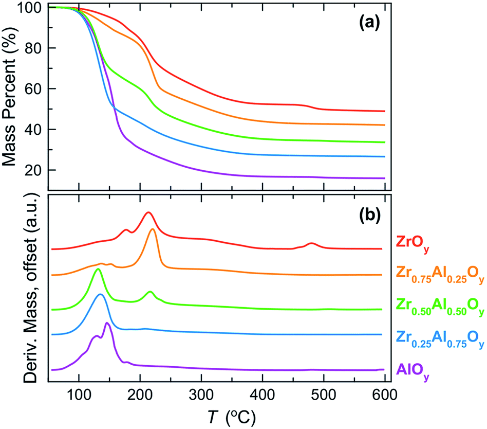 | ||
| Fig. 1 (a) Mass loss percent and (b) derivative of mass loss (absolute values) as a function of annealing temperature for bulk ZAO precursor powders. | ||
For the mixed ZAO precursor powders, increasing the Al content decreases both the decomposition temperature and the resulting oxide formation temperature. This trend is not surprising as it is known that metal nitrate decomposition temperatures decrease with increasing metal cation charge density.61 The higher charge density of Al3+ polarizes the nitrate ions, weakening N–O bond strengths and lowering decomposition temperatures for the Al-rich films.
TGA provides insight into the decomposition of the bulk precursor powders, but these measurements do not necessarily relate to the corresponding evolution of thin films due to differences in sample geometry, mass transport, and evaporation rates.62,63 Nevertheless, TGA is useful for providing approximate temperature ranges at which decomposition events take place and for correlating how these change with metal composition.
FTIR allows a direct measurement of water and nitrate content in ZAO films as a function of annealing temperature (Fig. 2). These spectra indicate that significant water (∼3500 cm−1)64 and nitrate (∼1280 and 1460 cm−1)31,65 are retained in films annealed at 200 °C (Fig. 2a). Al-rich films generally contain less nitrate, consistent with TGA data of bulk powders. Water is fully removed from films of all compositions by 400 °C (Fig. S1†), and nitrate is effectively removed by 500 °C (Fig. 2b).
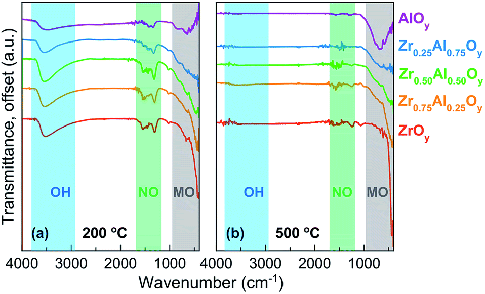 | ||
| Fig. 2 FTIR spectra of two-coat ZAO films annealed at (a) 200 °C and (b) 500 °C. FTIR spectra of ZAO films annealed at 300 and 400 °C can be found in Fig. S1.† | ||
Peaks indicative of Al–O (∼600 to 900 cm−1)31 and Zr–O (∼415 cm−1)41 are observed for the pure AlOy and ZrOy films, respectively. The intensity of these peaks increases for films annealed at higher temperatures, indicating oxide formation is more complete. Significant overlap and broadening of the metal oxide peaks makes identification of Al–O and Zr–O peaks in the mixed composition samples difficult.41 The loss of water and nitrate, coincident with growth of the oxide peak intensities, suggest that condensation is largely complete by 500 °C. XRR studies (which allow measurement of film thickness and density) also show that densification is complete by 500 °C (Fig. S2 and S3†).
As discussed above, amorphous metal oxides are preferred for gate oxide applications because grain boundaries in polycrystalline films negatively impact device performance.3,34 The extent of crystallization as a function of Zr:Al composition and annealing temperature was investigated using GIXRD (Fig. 3a and b). All compositions were amorphous at 400 °C, while ZrOy is crystalline by 500 °C. ZAO films with compositions of ≥25% Al are amorphous at 500 °C and remain so up to 600 °C. The minimum amount of Al needed to prevent crystallization at 500 °C was 10% Al, although these films crystallize by 600 °C.
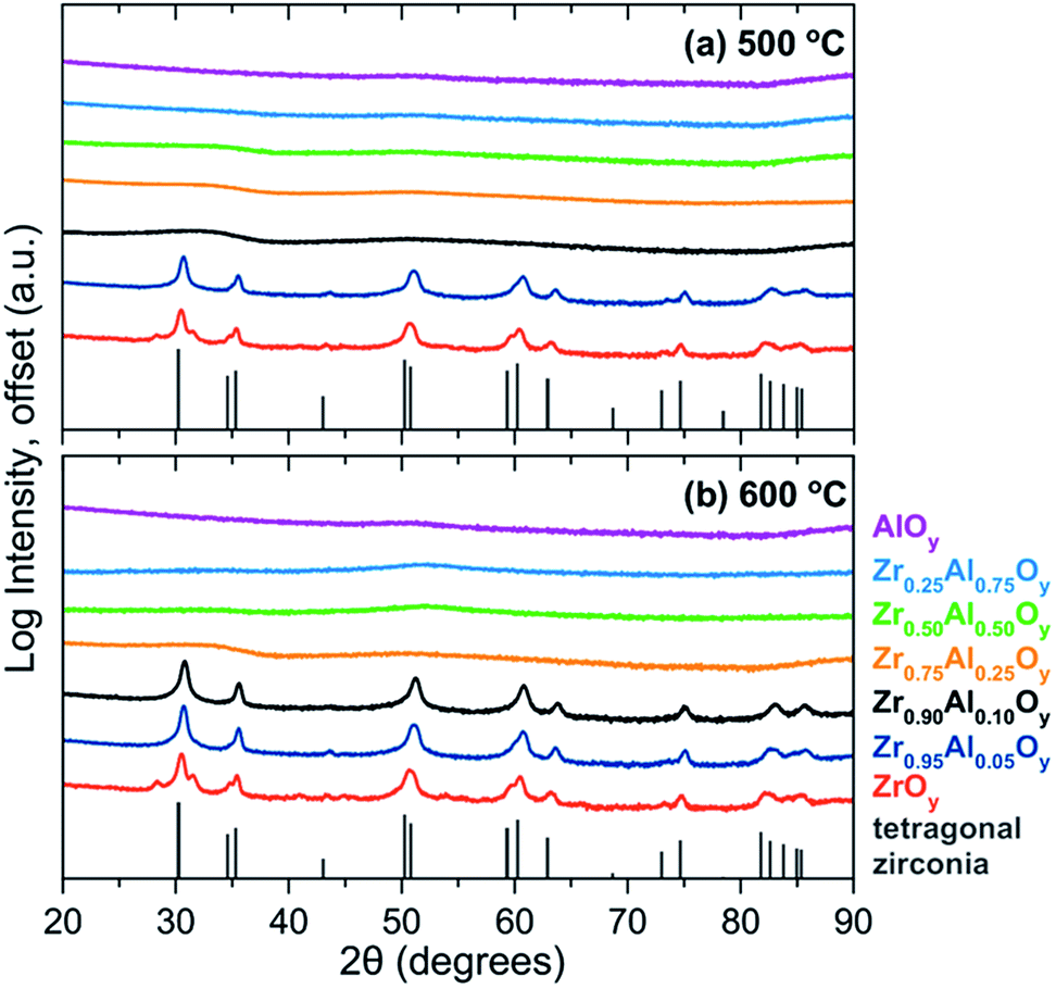 | ||
| Fig. 3 GIXRD of single-coat ZAO films annealed at (a) 500 °C and (b) 600 °C. The tetragonal zirconia phase (ICSD 66781)69 is plotted for reference. | ||
For many microelectronic applications, subnanometer surface roughness is essential for optimum device functionality.66–68 AFM shows ZAO films annealed at 500 °C (Fig. 4) are remarkably smooth (root-mean-square roughness (Rrms) < 1 nm). AlOy films, in particular, are exceptionally smooth with Rrms ≈ 0.1 nm (Fig. 4a). ZAO films with varying Zr:Al ratios are still quite smooth with Rrms ≈ 0.2–0.4 nm (Fig. 4b–e). In contrast, ZrOy films are significantly rougher (Rrms ≈ 0.8 nm). This increased roughness is likely associated with crystallization observed by GIXRD; indeed, crystallites are apparent in AFM images (Fig. 4f).
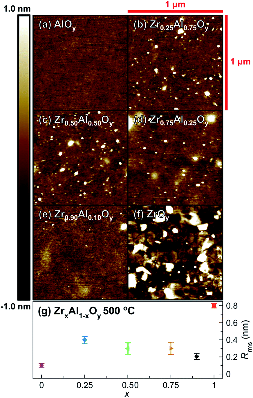 | ||
| Fig. 4 Representative AFM images of single-coat (a) AlOy, (b) Zr0.25Al0.75Oy, (c) Zr0.50Al0.50Oy, (d) Zr0.75Al0.25Oy, (e) Zr0.90Al0.10Oy, and (f) ZrOy films annealed at 500 °C (1 μm2 area) and (g) corresponding surface roughness values. Error bars were determined using measurements taken from three separate 1 μm2 areas on the same film. | ||
Cross-sectional SEM shows the morphology of stacked, two-coat ZAO films incorporated into MIS devices (Fig. 5). Amorphous ZAO films are dense and homogeneous, with no signs of interfacial roughness (Fig. 5a–c). In the case of crystalline ZrOy, large columnar grains are observed (Fig. 5d).
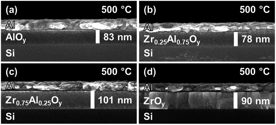 | ||
| Fig. 5 SEM cross-sectional images of two-coat (a) ZrOy, (b) Zr0.75Al0.25Oy, (c) Zr0.25Al0.75Oy, and (d) AlOy films annealed at 500 °C. | ||
MIS devices were fabricated from two-coat ZAO films, and dielectric properties were examined by impedance spectroscopy (Fig. 6 and S4†). Dielectric constants (1 kHz) increase with increasing Zr content, ranging from 5.4 (AlOy) to 18.6 (ZrOy) for films annealed at 600 °C. We attribute the large increases in dielectric constants and batch-to-batch variations for ZrOy films annealed at 500 °C and Zr0.90Al0.10Oy films annealed at 600 °C to the onset of crystallization (see Fig. 4). Generally, loss tangents were low, indicating minimal deviation from ideal capacitance (Fig. 6b).
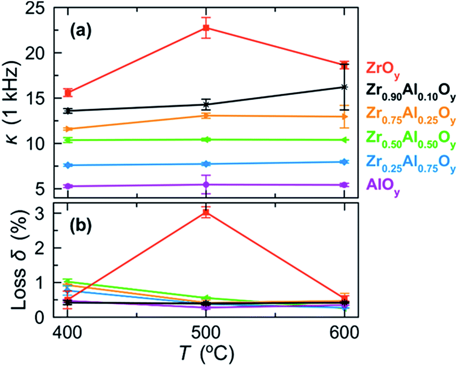 | ||
| Fig. 6 (a) Dielectric constants (κ) measured at 1 kHz and (b) corresponding loss tangents (loss δ) for MIS devices fabricated from two-coat (∼100 nm) ZAO films annealed at various temperatures. Error bars were determined using measurements taken from three separate batches of ZAO-based MIS devices. A plot of κ and loss δ as a function of frequency for ZAO-based MIS devices fabricated at 500 °C can be found in Fig. S4.† | ||
Although it is difficult to directly compare properties of materials deposited using different precursors and thermal treatments,63 the dielectric constants reported here are within the range of values reported in the literature. In a previous sol–gel study, Zr0.10Al0.90Oy films annealed between 250 and 350 °C for 2 h exhibited dielectric constants of 8.4 to 11.8.42 Although these values are larger than those reported here, they compare well to dielectric constant of Zr0.25Al0.75Oy films we prepared at 200 °C (κ ≈ 12) and 300 °C (κ ≈ 10). We do not include data for samples annealed at these low temperatures in Fig. 6 because FTIR data (Fig. 2 and S1†) indicate that these films contain residual polarizable water and nitrate, which can inflate dielectric constant values and lead to sample-to-sample variations.53 In a separate ultrasonic spray pyrolysis study, ZAO films with similar compositions and annealing temperatures (475 °C) are also in the range of those reported here.39
J–E measurements were conducted to assess the effects of Zr:Al composition on breakdown fields and leakage current densities of ZAO-based MIS devices processed at 500 °C (Fig. 7). In general, ZrxAl1−xOy devices experience catastrophic breakdown (defined as I > 100 mA) and loss of insulating behaviour at lower electric fields when x ≥ 0.90 (2.0 to 2.5 MV cm−1). In addition to lower breakdown voltages, batch-to-batch variation for Zr0.90Al0.10Oy devices was high, suggesting the formation of microcrystallites beneath the detection limit of GIXRD for these films. In contrast, devices fabricated from more Al-rich ZrxAl1−xOy films (x ≤ 0.25) experience breakdown at higher electric fields (∼3 MV cm−1), with AlOy devices breaking down at ∼3.7 MV cm−1.
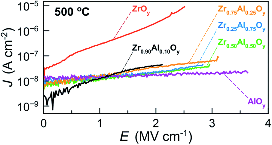 | ||
| Fig. 7 Representative JE data for MIS devices made from two-coat ZAO films (∼100 nm) annealed at 500 °C. | ||
Additionally, ZrOy-based MIS devices display the highest leakage current densities at all electric fields, in agreement with the relatively high loss δ measured for ZrOy-based devices annealed at 500 °C (Fig. 6b). We attribute this to the formation of crystallites and the presence of grain boundaries in films annealed at this temperature.34 Notably, incorporation of Al significantly decreases the leakage current densities of ZAO-based devices at all electric fields. ZrxAl1−xOy films with 0.25 ≤ x ≤ 0.90 show similar low leakage current densities, while AlOy films exhibit the lowest leakage current densities. Together, the MIS characterization suggests that Zr0.75Al0.25Oy displays the optimal balance of a high dielectric constant and low leakage current densities.
Conclusions
We report an all-inorganic aqueous deposition route to variable composition high-κ zirconium aluminium oxide films with sub-nm surface roughness and tunable properties. Residual nitrate and water are fully removed from ZAO films by 500 °C, and incorporation of Al ≥10% effectively suppresses crystallization of the tetragonal zirconia phase up to 500 °C. Dielectric constants increase with increasing Zr content, and films with Al >10% exhibit low leakage current densities. For the composition range studied, the combination of high dielectric constant and low leakage current densities makes Zr0.75Al0.25Oy a promising candidate for microelectronic applications.Conflicts of interest
There are no conflicts of interest to declare.Acknowledgements
This work was funded by the National Science Foundation Center for Sustainable Materials Chemistry (CSMC, Grant CHE-1606982). We gratefully acknowledge the use of UO CAMCOR High-Resolution and Nanofabrication Facility, which is supported by grants from the W. M. Keck Foundation, the M. J. Murdock Charitable Trust, ONAMI, the Air Force Research Laboratory (agreement FA8650-05-1-5041), NSF (Awards 0923577 and 0421086), and the University of Oregon. The authors thank Matthew G. Kast, Julija Vinckevičiūtė, and Paul N. Plassmeyer for preliminary studies and helpful discussions. This research was conducted as part of the 2016 CSMC Summer Materials Research Training (SMaRT) program and we thank the staff, graduate student mentors, and undergraduate participants.References
- J. Robertson, Rep. Prog. Phys., 2006, 69, 327–396 CrossRef CAS.
- E. Fortunato, P. Barquinha and R. Martins, Adv. Mater., 2012, 24, 2945–2986 CrossRef CAS PubMed.
- G. D. Wilk, R. M. Wallace and J. M. Anthony, J. Appl. Phys., 2001, 89, 5243–5275 CrossRef CAS.
- J. P. Maria, D. Wicaksana, A. I. Kingon, B. Busch, H. Schulte, E. Garfunkel and T. Gustafsson, J. Appl. Phys., 2001, 90, 3476–3482 CrossRef CAS.
- K. Kukli, K. Forsgren, M. Ritala, M. Leskelä, J. Aarik and A. Hårsta, J. Electrochem. Soc., 2001, 148, F227–F232 CrossRef CAS.
- G. Adamopoulos, S. Thomas, P. H. Wöbkenberg, D. D. C. Bradley, M. A. McLachlan and T. D. Anthopoulos, Adv. Mater., 2011, 23, 1894–1898 CrossRef CAS PubMed.
- L. Xifeng, X. Enlong and Z. Jianhua, IEEE Trans. Electron Devices, 2013, 60, 3413–3416 CrossRef.
- J. H. Park, Y. B. Yoo, K. H. Lee, W. S. Jang, J. Y. Oh, S. S. Chae and H. K. Baik, ACS Appl. Mater. Interfaces, 2013, 5, 410–417 CAS.
- Y. M. Park, A. Desai, A. Salleo and L. Jimison, Chem. Mater., 2013, 25, 2571–2579 CrossRef CAS.
- J. Jang, R. Kitsomboonloha, S. L. Swisher, E. S. Park, H. Kang and V. Subramanian, Adv. Mater., 2013, 25, 1042–1047 CrossRef CAS PubMed.
- A. Liu, G. X. Liu, H. H. Zhu, F. Xu, E. Fortunato, R. Martins and F. K. Shan, ACS Appl. Mater. Interfaces, 2014, 6, 17364–17369 CAS.
- G. X. Liu, A. Liu, F. K. Shan, Y. Meng, B. C. Shin, E. Fortunato and R. Martins, Appl. Phys. Lett., 2014, 105, 113509 CrossRef.
- C. Zhu, A. Liu, G. Liu, G. Jiang, Y. Meng, E. Fortunato, R. Martins and F. Shan, J. Mater. Chem. C, 2016, 4, 10715–10721 RSC.
- W. He, W. Xu, Q. Peng, C. Liu, G. Zhou, S. Wu, M. Zeng, Z. Zhang, J. Gao, X. Gao, X. Lu and J.-M. Liu, J. Phys. Chem. C, 2016, 120, 9949–9957 CAS.
- C. Avis and J. Jang, J. Mater. Chem., 2011, 21, 10649–10652 RSC.
- T. Lim, D. Kim and S. Ju, Appl. Phys. Lett., 2013, 103, 13107 CrossRef.
- Y. Liu, P. Guan, B. Zhang, M. L. Falk and H. E. Katz, Chem. Mater., 2013, 25, 3788–3796 CrossRef CAS.
- J. H. Park, K. Kim, Y. B. Yoo, S. Y. Park, K.-H. Lim, K. H. Lee, H. K. Baik and Y. S. Kim, J. Mater. Chem. C, 2013, 1, 7166–7174 RSC.
- P. K. Nayak, M. N. Hedhili, D. Cha and H. N. Alshareef, Appl. Phys. Lett., 2013, 103, 33518 CrossRef.
- H. J. Ha, S. W. Jeong, T.-Y. Oh, M. Kim, K. Choi, J. H. Park and B.-K. Ju, J. Phys. D: Appl. Phys., 2013, 46, 235102 CrossRef.
- E. J. Bae, Y. H. Kang, M. Han, C. Lee and S. Y. Cho, J. Mater. Chem. C, 2014, 2, 5695–5703 RSC.
- L. Y. Liang, H. T. Cao, Q. Liu, K. M. Jiang, Z. M. Liu, F. Zhuge and F. L. Deng, ACS Appl. Mater. Interfaces, 2014, 6, 2255–2261 CAS.
- G. Huang, L. Duan, G. Dong, D. Zhang and Y. Qiu, ACS Appl. Mater. Interfaces, 2014, 6, 20786–20794 CAS.
- H. Wang, T. Sun, W. Xu, F. Xie, L. Ye, Y. Xiao, Y. Wang, J. Chen and J. Xu, RSC Adv., 2014, 4, 54729–54739 RSC.
- Y. S. Rim, H. Chen, Y. Liu, S.-H. Bae, H. J. Kim and Y. Yang, ACS Nano, 2014, 8, 9680–9686 CrossRef CAS PubMed.
- R. Branquinho, D. Salgueiro, L. Santos, P. Barquinha, L. Pereira, R. Martins and E. Fortunato, ACS Appl. Mater. Interfaces, 2014, 6, 19592–19599 CAS.
- H. Park, Y. Nam, J. Jin and B.-S. Bae, RSC Adv., 2015, 5, 102362–102366 RSC.
- R. Branquinho, D. Salgueiro, A. Santa, A. Kiazadeh, P. Barquinha, L. Pereira, R. Martins and E. Fortunato, Semicond. Sci. Technol., 2015, 30, 24007 CrossRef.
- H. Tan, G. Liu, A. Liu, B. Shin and F. Shan, Ceram. Int., 2015, 41, S349–S355 CrossRef CAS.
- A. Liu, G. Liu, H. Zhu, B. Shin, E. Fortunato, R. Martins and F. Shan, RSC Adv., 2015, 5, 86606–86613 RSC.
- W. Xu, H. Wang, F. Xie, J. Chen, H. Cao and J.-B. Xu, ACS Appl. Mater. Interfaces, 2015, 7, 5803–5810 CAS.
- Y. S. Rim, H. Chen, T.-B. Song, S.-H. Bae and Y. Yang, Chem. Mater., 2015, 27, 5808–5812 CrossRef CAS.
- W. Xu, M. Long, T. Zhang, L. Liang, H. Cao, D. Zhu and J.-B. Xu, Ceram. Int., 2017, 43, 6130–6137 CrossRef CAS.
- K. Jiang, J. T. Anderson, K. Hoshino, D. Li, J. F. Wager and D. A. Keszler, Chem. Mater., 2011, 23, 945–952 CrossRef CAS.
- J. Zhu and Z. G. Liu, Microelectron. Eng., 2003, 66, 849–854 CrossRef CAS.
- Y. Li, J. Zhu, H. Liu and Z. Liu, Microelectron. Eng., 2006, 83, 1905–1911 CrossRef CAS.
- D. Zhou, U. Schroeder, G. Jegert, M. Kerber, S. Uppal, R. Agaiby, M. Reinicke, J. Heitmann and L. Oberbeck, J. Appl. Phys., 2009, 106, 44104 CrossRef.
- D. Zhou, U. Schroeder, J. Xu, J. Heitmann, G. Jegert, W. Weinreich, M. Kerber, S. Knebel, E. Erben and T. Mikolajick, J. Appl. Phys., 2010, 108, 124104 CrossRef.
- M. Bizarro, J. C. Alonso and A. Ortiz, J. Electrochem. Soc., 2005, 152, F179 CrossRef.
- M. Bizarro, J. C. Alonso and A. Ortiz, Mater. Sci. Semicond. Process., 2006, 9, 1090–1096 CrossRef CAS.
- P. Vitanov, A. Harizanova, T. Ivanova, C. Trapalis and N. Todorova, Mater. Sci. Eng., B, 2009, 165, 178–181 CrossRef CAS.
- W. Yang, K. Song, Y. Jung, S. Jeong and J. Moon, J. Mater. Chem. C, 2013, 1, 4275–4282 RSC.
- S. R. Thomas, P. Pattanasattayavong and T. D. Anthopoulos, Chem. Soc. Rev., 2013, 42, 6910–6923 RSC.
- S. Park, C.-H. Kim, W.-J. Lee, S. Sung and M.-H. Yoon, Mater. Sci. Eng., R, 2017, 114, 1–22 CrossRef.
- Q. Fan, B. McQuillin, A. K. Ray, M. L. Turner and A. B. Seddon, J. Phys. D: Appl. Phys., 2000, 33, 2683–2686 CrossRef CAS.
- Z. Wang, U. Helmersson and P.-O. Käll, Thin Solid Films, 2002, 405, 50–54 CrossRef CAS.
- J. T. Anderson, C. L. Munsee, C. M. Hung, T. M. Phung, G. S. Herman, D. C. Johnson, J. F. Wager and D. A. Keszler, Adv. Funct. Mater., 2007, 17, 2117–2124 CrossRef CAS.
- S. T. Meyers, J. T. Anderson, D. Hong, C. M. Hung, J. F. Wager and D. A. Keszler, Chem. Mater., 2007, 19, 4023–4029 CrossRef CAS.
- M. Alemayehu, J. E. Davis, M. Jackson, B. Lessig, L. Smith, J. D. Sumega, C. Knutson, M. Beekman, D. C. Johnson and D. A. Keszler, Solid State Sci., 2011, 13, 2037–2040 CrossRef CAS.
- K. Jiang, S. T. Meyers, M. D. Anderson, D. C. Johnson and D. A. Keszler, Chem. Mater., 2013, 25, 210–214 CrossRef CAS.
- R. P. Oleksak, W. F. Stickle and G. S. Herman, J. Mater. Chem. C, 2015, 3, 3114–3120 RSC.
- A. Nadarajah, M. Z. B. Wu, K. Archila, M. G. Kast, A. M. Smith, T. H. Chiang, D. A. Keszler, J. F. Wager and S. W. Boettcher, Chem. Mater., 2015, 27, 5587–5596 CrossRef CAS.
- P. N. Plassmeyer, K. Archila, J. F. Wager and C. J. Page, ACS Appl. Mater. Interfaces, 2015, 7, 1678–1684 CAS.
- K. M. Norelli, P. N. Plassmeyer, K. N. Woods, B. A. Glassy, C. C. Knutson, M. Beekman and C. J. Page, Solid State Sci., 2016, 55, 8–12 CrossRef CAS.
- K. N. Woods, T.-H. Chiang, P. N. Plassmeyer, M. G. Kast, A. C. Lygo, A. K. Grealish, S. W. Boettcher and C. J. Page, ACS Appl. Mater. Interfaces, 2017, 9, 10897–10903 CAS.
- K. M. Kim, C. W. Kim, J. S. Heo, H. Na, J. E. Lee, C. B. Park, J.-U. Bae, C.-D. Kim, M. Jun, Y. K. Hwang, S. T. Meyers, A. Grenville and D. A. Keszler, Appl. Phys. Lett., 2011, 99, 242109 CrossRef.
- S. W. Smith, W. Wang, D. A. Keszler and J. F. Conley, J. Vac. Sci. Technol., A, 2014, 32, 41501 Search PubMed.
- M. G. Kast, E. A. Cochran, L. J. Enman, G. Mitchson, J. Ditto, C. Siefe, P. N. Plassmeyer, A. L. Greenaway, D. C. Johnson, C. J. Page and S. W. Boettcher, J. Am. Chem. Soc., 2016, 138, 16800–16808 CrossRef CAS PubMed.
- M. Wormington, C. Panaccione, K. M. Matney and D. K. Bowen, Philos. Trans. R. Soc., A, 1999, 357, 2827–2848 CrossRef CAS.
- K. H. Kim, Z. Akase, T. Suzuki and D. Shindo, Mater. Trans., 2010, 51, 1080–1083 CrossRef CAS.
- S. Yuvaraj, L. Fan-Yuan, C. Tsong-Huei and Y. Chuin-Tih, J. Phys. Chem. B, 2003, 107, 1044–1047 CrossRef CAS.
- P. Roura, J. Farjas, H. Eloussifi, L. Carreras, S. Ricart, T. Puig and X. Obradors, Thermochim. Acta, 2015, 601, 1–8 CrossRef CAS.
- S. R. Wood, K. N. Woods, P. N. Plassmeyer, D. A. Marsh, D. W. Johnson, C. J. Page, K. M. Ø. Jensen and D. C. Johnson, J. Am. Chem. Soc., 2017, 139, 5607–5613 CrossRef CAS PubMed.
- H. A. Al-Abadleh and V. H. Grassian, Langmuir, 2003, 19, 341–347 CrossRef CAS.
- R. A. Nyquist, C. L. Putzig, M. A. Leugers and R. O. Kagel, The Handbook of Infrared and Raman Spectra of Inorganic Compounds and Organic Salts, Academic Press, San Diego, CA, USA, 1997 Search PubMed.
- Y. Jung, R. J. Kline, D. A. Fischer, E. K. Lin, M. Heeney, I. McCulloch and D. M. DeLongchamp, Adv. Funct. Mater., 2008, 18, 742–750 CrossRef CAS.
- J.-M. Lee, B.-H. Choi, M.-J. Ji, J.-H. Park, J.-H. Kwon and B.-K. Ju, Semicond. Sci. Technol., 2009, 24, 55008 CrossRef.
- N. Alimardani, E. W. Cowell III, J. F. Wager, J. F. Conley Jr, D. R. Evans, M. Chin, S. J. Kilpatrick and M. Dubey, J. Vac. Sci. Technol., A, 2012, 30, 01A113 Search PubMed.
- B. Bondars, G. Heidemane, J. Grabis, K. Laschke, H. Boysen, J. Schneider and F. Frey, J. Mater. Sci., 1995, 30, 1621–1625 CrossRef CAS.
Footnote |
| † Electronic supplementary information (ESI) available: Fourier transform infrared (FTIR) spectra, X-ray reflectivity (XRR) data and best fit models, film thicknesses and densities from XRR best fit models, dielectric constant dispersion data. See DOI: 10.1039/c7ra08362a |
| This journal is © The Royal Society of Chemistry 2017 |