
 Open Access Article
 This Open Access Article is licensed under a
 Creative Commons Attribution 3.0 Unported Licence
Direct fabrication of electrochromic devices with complex patterns on three-dimensional substrates using polymeric stencil films†
Seokwon Joo a,
Ju-Hyung Kim*b and
Soonmin Seo*a
a,
Ju-Hyung Kim*b and
Soonmin Seo*a
aCollege of BioNano Technology, Gachon University, Gyeonggi 13120, Republic of Korea. E-mail: soonmseo@gachon.ac.kr
bDepartment of Chemical Engineering, Ajou University, Suwon 16499, Republic of Korea. E-mail: juhyungkim@ajou.ac.kr
First published on 7th September 2017
Abstract
We present a direct fabrication technique for electrochromic devices with complex shapes including weakly supported and unsupported patterns on three-dimensional (3D) substrates. For this work, we employed freestanding polymeric stencil films as shadow masks, and performed two-step shadow masking processes. Using this technique, not only flexible materials but also rigid materials such as metals and other inorganic materials can be directly deposited onto non-flat substrates, realising complex shapes and high uniformity. Weakly supported and even unsupported patterns (i.e., island and ring shapes) of rigid materials were successfully achieved on both flat and non-flat substrates. Eventually, electrochromic display devices based on tungsten trioxide (WO3) with various shapes were also demonstrated on the 3D substrates as well. We anticipate that this fabrication technique will significantly contribute to the development of various integrated thin-film devices on complex-structured substrates, which may lead to further applications.
Introduction
In the past few decades, flexible electronics has attracted a lot of interest due to the development and advancement of thin-film devices,1–5 and unconventional functionalities associated with flexible electronics such as stretchability, wearability and patchability are also receiving much attention for further applications.6–16 Flexible electronics has been actively applied to the field of display devices in particular, and curved display panels have already been commercialised along with remarkable improvements in materials and fabrication processes for thin-film devices. Fabrication techniques for thin-film devices of great potential have advanced considerably to realise non-flat device configurations. However, since electrode layers in thin-film devices are mostly deposited by thermal evaporation of metals through rigid shadow masks, there has been trouble with producing uniform electrode layers directly on non-flat substrates. In this context, a novel technique to fabricate organic devices on complex-structured substrates was recently reported using polymeric perforated films as shadow masks with high flexibility and adhesive properties.17,18 Although minute perforated patterns can be easily achieved on the polymeric films within a few tens of μm range via this technique, weakly supported patterns such as perforated vortex shapes and stripes with high aspect ratios are rather limited due to the flexible nature of polymers. It is worth noting that polydimethylsiloxane (PDMS) and polyurethane acrylate (PUA) are widely used to fabricate the polymeric perforated films.17–21 While several classes of polymers such as polyimide and polymethyl-vinyl siloxane show excellent environmental stabilities and mechanical properties as substrate materials in flexible electronics,22,23 PDMS and PUA provide proper material characteristics for polymer patterning (i.e., soft lithography) owing to their low moduli and surface energies enabling conformal contact and easy release.24–26Here we present a direct fabrication technique for electrode layers and further electrochromic devices with complex shapes including weakly supported and unsupported patterns on three-dimensional (3D) substrates. For this work, we employed freestanding polymeric stencil films, and performed two-step shadow masking processes.17,27–30 Using this technique, not only flexible materials but also rigid materials such as metals and other inorganic materials can be directly deposited onto non-flat substrates with realising various patterns and high uniformity. Weakly supported and even unsupported patterns (i.e., island and ring shapes) of rigid materials were successfully achieved on both flat and non-flat substrates. Eventually, we demonstrate the fabrication and operation of electrochromic display devices with complex shapes on the 3D substrates.31–33 These results strongly suggest potential for the further development of various thin-film devices on complex-structured substrates including display devices and smart window applications.
Experimental
Preparation of polymeric perforated films
Preparation procedure of the polymeric stencil films is schematically illustrated in Fig. 1. A photoresist (SU-8 1075) layer with a thickness of 150 μm was prepared on the SiO2 wafer and engraved with the desired structural design following a conventional photolithography method.27,34 The patterned SU-8 layer was negatively replicated using PDMS (Sylgard 184, tensile modulus = 1.6 MPa, elongation at break = 146%). An ultra-violet (UV) curable PUA mixture, which was synthesised in accordance with the previous reports,24–26 was then drop-dispensed onto the PDMS replica with the embossed pattern of desired structure, and it was subsequently covered with another flat PDMS mould. The excess amount of the PUA mixture between the two PDMS moulds was squeezed out using a roller until the embossed PDMS pattern was brought into contact with the flat PDMS mould. The sample was exposed to UV light (λ ∼ 365 nm) for 10 minutes, and the PUA mixture was cured though the transparent PDMS moulds. After the UV curing, the two PDMS moulds were easily peeled off from the sample due to low surface energies of both PDMS (∼21.6 mJ m−2) and PUA (∼23.0 mJ m−2),24–26 and consequently a freestanding PUA film with the desired stencil-pattern was prepared. Note that soft PUA films with high flexibility ensure conformal contact with complex-structured substrates, and remaining unsaturated acrylate after the UV curing provides adhesive properties. It has been known that the soft PUA material has a tensile modulus of ∼19.8 MPa, and elongation at break of 45%.24–26 In addition, since the absence of residual PUA within the contact area of the two PDMS moulds is necessary for the fabrication of the stencil-pattern, the resolution of the stencil-pattern is limited in a few tens of μm range without external pressure.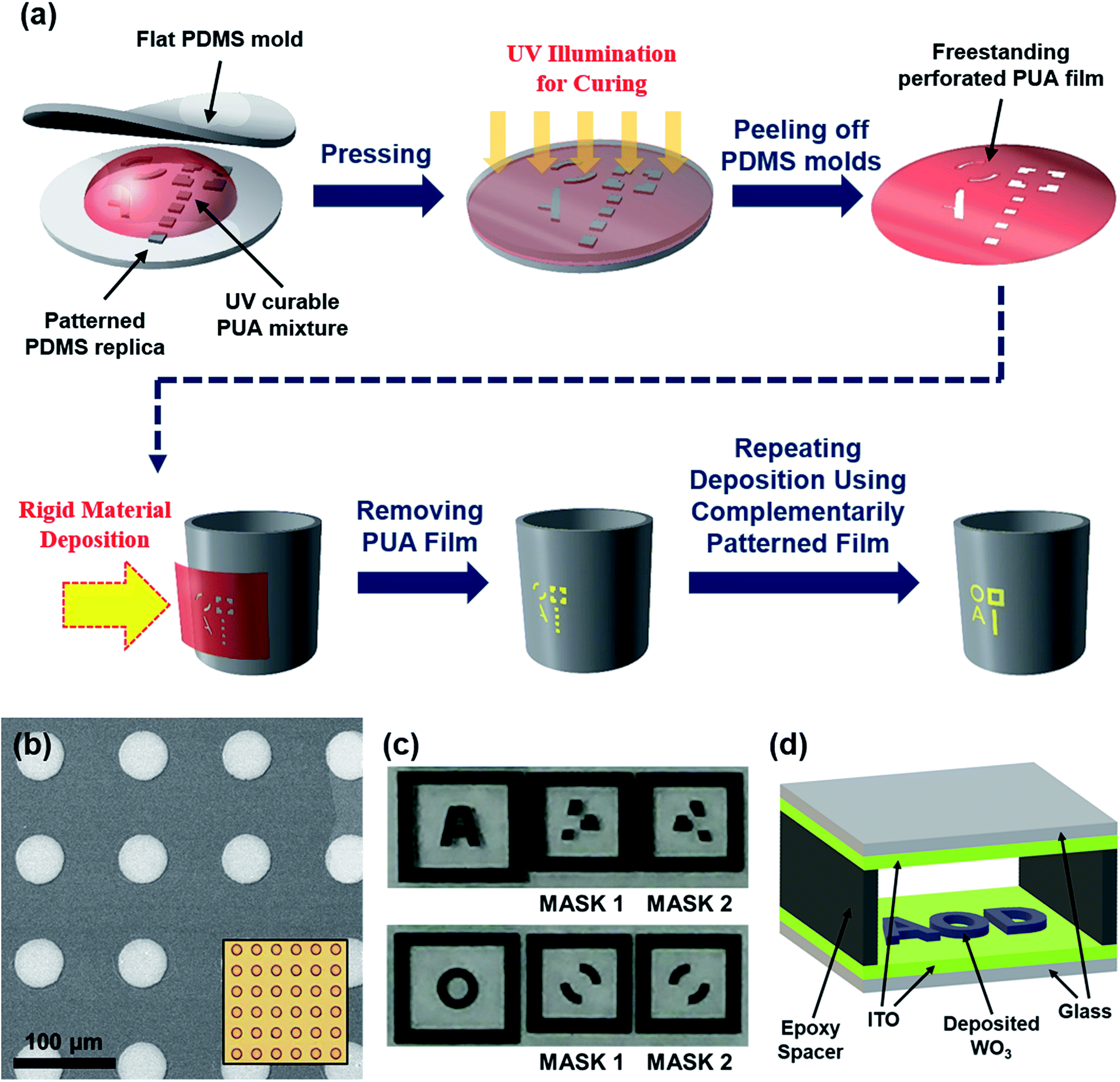 | ||
| Fig. 1 (a) Schematic illustration of the preparation of polymeric stencil film and the two-step shadow masking process. (b) Scanning electron microscopy (SEM) image of the deposited WO3 (200 nm) on a glass substrate prepared as illustrated in (a) [inset: optical microscopy image of the PUA stencil film used as a shadow mask. The diameter of each motif is 50 μm]. (c) Photographs of the photomasks with unsupported patterns, ‘A’ and ‘O’. Each unsupported pattern consists of two complementary patterns (designated “MASK 1” and “MASK 2”, respectively). (d) Configuration of electrochromic display device. The gap space between two ITO-coated glasses is filled with an electrolyte solution by syringe injection to complete the device structure. | ||
Two-step shadow masking processes for weakly supported and unsupported patterns
The freestanding PUA stencil films exhibit high flexibility and adhesive properties originating from remaining unsaturated acrylate in cured PUA, enabling conformal contact with various complex-structured substrates. Thus, the freestanding PUA stencil films were used as shadow masks for thermal evaporation, and two-step shadow masking processes were also performed to achieve weakly supported (i.e., long and narrow shapes) and unsupported patterns (i.e., island and ring shapes) of rigid materials on various substrates. Fig. 1(b) shows an exemplary pattern of tungsten trioxide (WO3, 200 nm) deposited using the freestanding PUA stencil film (of 50 μm thickness). The diameter of each motif was 50 μm, and the fine structures were successfully achieved with clean edges. For the two-step shadow masking process, the desired pattern was divided into two complementary patterns as shown in Fig. 1(c), and two PUA stencil films (designated “MASK 1” and “MASK 2”, respectively) were individually prepared corresponding to the patterns. Differently from the originally desired pattern, perforations of both complementary patterns were strongly supported by the PUA backbones, facilitating shadow masking processes without significant structural deformation. In a vacuum chamber, rigid material (i.e., metal or other inorganic material) was thermally deposited through the MASK 1, which was in conformally contact with the substrate. The thickness of the coated films in our deposition range (from 70 nm to 300 nm) was highly compatible to 50 μm- and 150 μm-thick masks.17 After peeling off the MASK 1, the MASK 2 was aligned onto the substrate to complete the originally desired pattern, and the thermal deposition process was sequentially repeated onto it. Since PUA is transparent, and because the dimension of each mask is identical, an accurate alignment of the mask is feasible using an optical microscope. If two arbitrary selected edges of the MASK 2 are first aligned to the deposited pattern edges, a simultaneous alignment of the mask can be achieved by careful attachment of the remaining part of the mask onto the substrate.Fabrication of electrochromic display devices
Electrochromic display devices were directly fabricated on glass substrates coated with indium-tin-oxide (ITO), as schematically illustrated in Fig. 1(d). On the ITO-coated glass, WO3 was deposited to form the desired pattern, following the same deposition procedure as described above. The prepared sample with the patterned WO3 was then covered with another ITO-coated glass, and adhesive epoxy was used for a fixed gap space (1.0 mm) between the two ITO-coated glasses. The gap space was filled with an electrolyte solution (0.1 M of LiClO4 in propylene carbonate) by syringe injection to complete the device structure.Results and discussion
Two-step shadow masking processes using the PUA stencil films facilitate the deposition of rigid materials in the shapes of weakly supported and unsupported patterns on various substrates. Since unsupported shapes of perforations are not patternable, and because weakly supported patterns of the freestanding PUA stencil films are easily deformed, the complementary patterns which are strongly supported by the PUA backbones can be employed as alternative shadow masks to achieve complex deposition patterns. In addition, the freestanding PUA stencil films enable conformal contact with various complex-structured substrates, facilitating direct deposition onto the 3D substrates. Unsupported patterns of gold (Au) and silver (Ag) such as ‘A’ and ‘O’ were easily achieved on cylindrical glass bottles via two-step shadow masking as shown in Fig. 2, to which one-step deposition processes are not applicable. This two-step shadow masking method also can lead to realisation of more complicated patterns such as character string and rose symbol (see Fig. 2).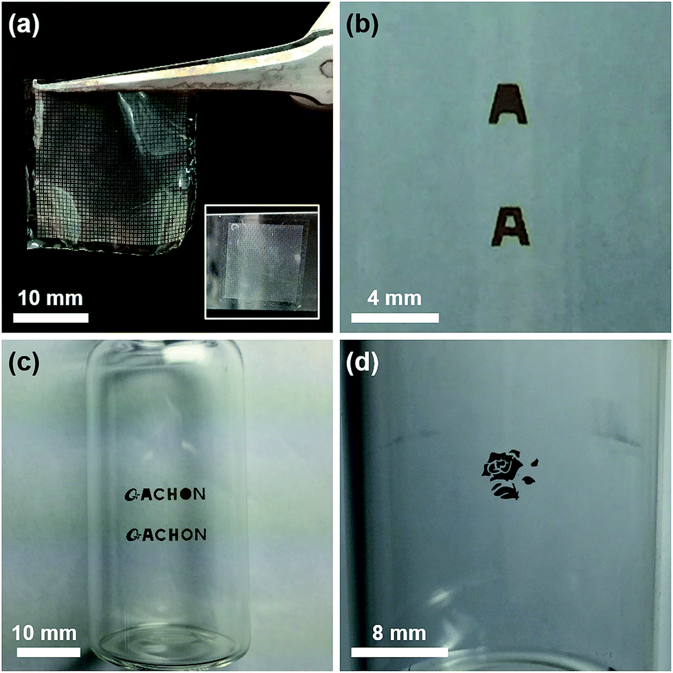 | ||
| Fig. 2 (a) Photograph of the freestanding PUA stencil film [inset: photograph of (a) in contact with a glass substrate]. (b) Photograph of the island patterns of Au deposited by one-step (upper) and two-step (lower) shadow masking processes, respectively. (c) Photograph of the character string patterns of Au deposited on a cylindrical glass bottle by one-step (upper) and two-step (lower) shadow masking processes, respectively. (d) Photograph of the rose symbol pattern of Ag deposited on a cylindrical glass bottle by two-step shadow masking process. | ||
Fig. 3 shows a demonstration of fabricating the electrochromic display devices with complex shapes consisting of complementary patterns. For this work, WO3 was used as an electrochromic material, of which colour changes during oxidation and reduction in the LiClO4 solution as follows: WO3 (transparent) + Li+ + e− ↔ LiWO3 (dark blue).35 Such reversible oxidation and reduction reactions are clearly revealed in hysteretic current-versus-voltage (I–V) characteristics as indicated in Fig. 3(d). Firstly, the electrochromic display devices were fabricated on the flat ITO-coated glasses (20 Ω □−1) via two-step shadow masking processes, allowing various electrochromic patterns in complex shapes as shown in Fig. 3. When the sample bias voltage between the two ITO electrodes was kept at −3.0 V (i.e., WO3/ITO is a cathode), the electrochromic response time was measured to be less than a second. It is worth noting that colouration contrast can be introduced in the electrochromic display as clearly indicated in Fig. 3(a). Light transmittance of WO3 significantly varies with the film thickness (see Fig. 3(e)). Under white light illumination, the relative transmittivities of WO3 after (before) changing colour were measured to be 48.0% (85.5%) for 100 nm-thick film, 28.9% (83.6%) for 200 nm-thick film, and 21.7% (80.3%) for 300 nm-thick film, respectively. Thus, if more than two complementary patterns of WO3 are deposited with different thicknesses through the PUA stencil masks, colouration contrast of the completed pattern can be easily presented in the electrochromic display. Secondly, reversible switching of two electrochromic display patterns was demonstrated (see Fig. 3(b) and ESI for movies†). Two electrochromic patterns of WO3 (∼100 nm) were individually prepared on the ITO-coated glasses, and placed facing each other with a fixed gap space (1.0 mm) using adhesive epoxy. The gap space between the two patterns was then filled with the LiClO4 solution. Since the cathode side of the device is reversibly changed corresponding to the sign of the potential difference between the two ITO glasses, the oxidised WO3 and the reduced LiWO3 patterns also can be reversibly switched. Thus, when one ITO side was grounded and the other was biased with voltage, the two electrochromic patterns were opposingly coloured and bleached according to the sign of voltage (i.e., +3.0 V and −3.0 V, respectively). Finally, the electrochromic display device was directly fabricated on a cylindrical bottle substrate (see Fig. 3(c) and ESI for Movies†). Thin ITO films were coated on both polyethylene terephthalate (PET) and cylindrical bottle (of 25.0 mm radius) substrates by sputtering. The electrochromic pattern of WO3 (i.e., university emblem) was deposited on the ITO-coated bottle using the freestanding perforated PUA film, and then covered with the flexible ITO-coated PET film. After completing the device configuration with the electrolyte, the electrochromic response time of WO3 was measured to be a few seconds. Note that such slow response time possibly originates from high resistance of each ITO electrode, which is expected to be efficiently enhanced by optimizing sputtering conditions.
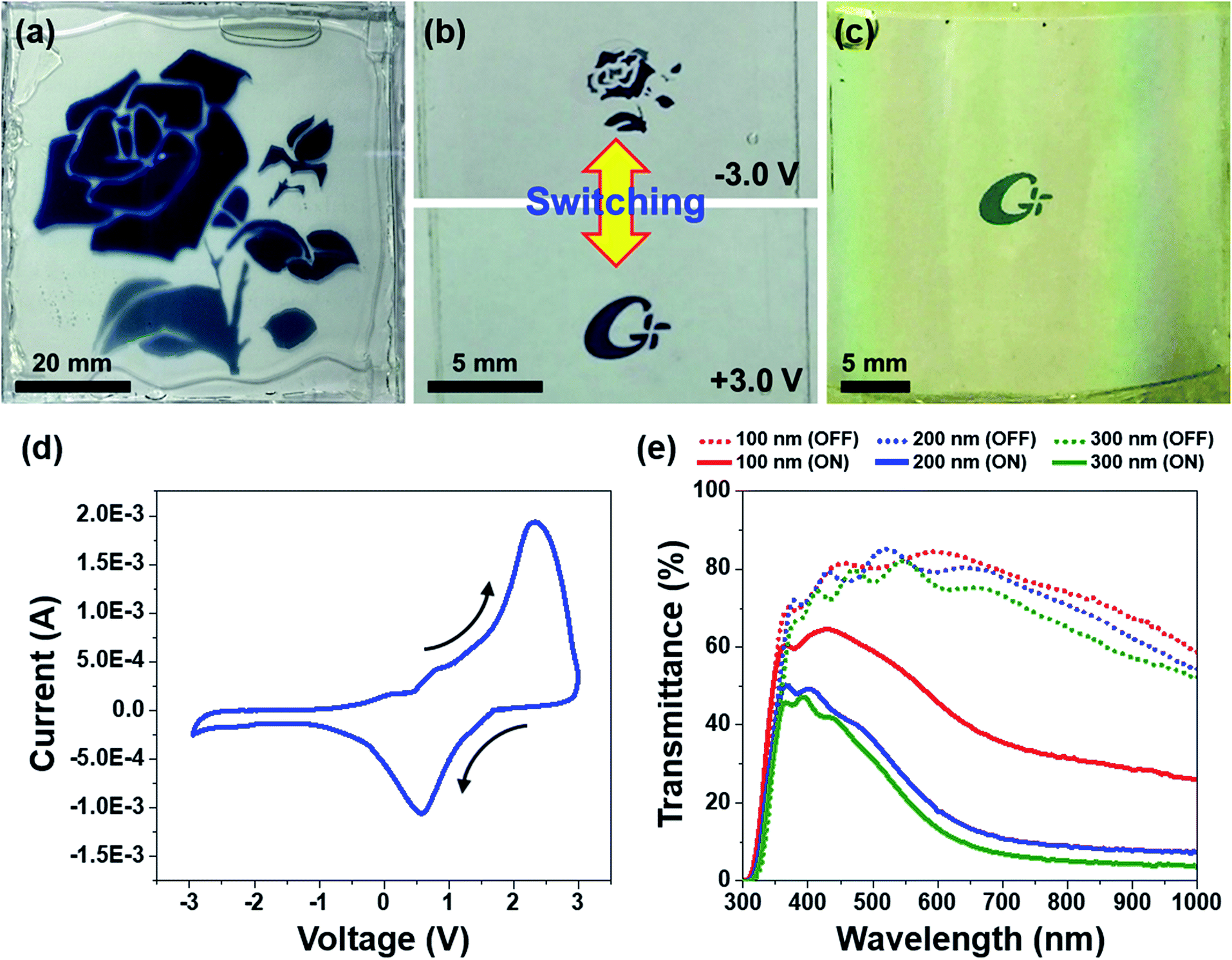 | ||
| Fig. 3 (a) Photograph of the electrochromic device displaying the rose symbol pattern. Complementary WO3 patterns with different thicknesses (100 nm, 200 nm, and 300 nm) were used to introduce colouration contrast in the display. (b) Reversible switching of two electrochromic display patterns. If one ITO side is grounded and the other is biased with voltage, the two electrochromic patterns can be opposingly coloured and bleached corresponding to the sign of voltage. (c) Photograph of the electrochromic display device directly fabricated on a cylindrical bottle substrate. The electrochromic pattern of WO3 (i.e., university emblem) was deposited on the ITO-coated bottle using the freestanding PUA stencil film. (d) Hysteretic current-versus-voltage (I–V) characteristics of the electrochromic display device. The 300 nm-thick WO3 film was used as an electrochromic layer. (e) Light transmittances of the WO3 films with varied thicknesses before (designated “OFF”) and after (designated “ON”) changing colour of WO3, in the range 300 to 1000 nm. | ||
Conclusions
In conclusion, we demonstrate the direct fabrication of electrode layers and electrochromic display devices with complex shapes including weakly supported and unsupported patterns on both flat and non-flat substrates. Technically, two complementary perforated patterns composing the desired complex structure were individually prepared on the PUA films, and sequentially used for two-step shadow masking. The PUA films accomplish conformal contact with complex-structured substrates, enabling direct deposition of various rigid materials with high uniformity. Eventually, electrochromic display devices based on WO3 with complex shapes were directly fabricated and operated on both flat and non-flat substrates, and distinctive features such as colouration contrast and reversible switching were successfully introduced into the devices as well. In consideration of a wide range of electrochromic applications, these results strongly suggest great potential for more diversified 3D electrochromic devices.Conflicts of interest
There are no conflicts to declare.Acknowledgements
This research was supported by Basic Science Research Program through the National Research Foundation of Korea funded by the Ministry of Education (NRF-2015R1D1A1A01060065 and NRF-2015R1D1A1A01060089).References
- D.-H. Kim, Y.-S. Kim, J. Wu, Z. Liu, J. Song, H.-S. Kim, Y. Y. Huang, K.-C. Hwang and J. A. Rogers, Adv. Mater., 2009, 21, 3703–3707 CrossRef CAS.
- T. Sekitani, H. Nakajima, H. Maeda, T. Fukushima, T. Aida, K. Hata and T. Someya, Nat. Mater., 2009, 8, 494–499 CrossRef CAS PubMed.
- T. Sekitani, U. Zschieschang, H. Klauk and T. Someya, Nat. Mater., 2010, 9, 1015–1022 CrossRef CAS PubMed.
- M. Kaltenbrunner, M. S. White, E. D. Głowacki, T. Sekitani, T. Someya, N. S. Sariciftci and S. Bauer, Nat. Commun., 2012, 3, 770 CrossRef PubMed.
- M. S. White, M. Kaltenbrunner, E. D. Głowacki, K. Gutnichenko, G. Kettlgruber, I. Graz, S. Aazou, C. Ulbricht, D. A. Egbe, M. C. Miron, Z. Major, M. C. Scharber, T. Sekitani, T. Someya, S. Bauer and N. S. Sariciftci, Nat. Photonics, 2013, 7, 811–816 CrossRef CAS.
- D.-H. Kim, J.-H. Ahn, W. M. Choi, H.-S. Kim, T.-H. Kim, J. Song, Y. Y. Huang, Z. Liu, C. Lu and J. A. Rogers, Science, 2008, 320, 507–511 CrossRef CAS PubMed.
- J. A. Rogers, T. Someya and Y. Huang, Science, 2010, 327, 1603–1607 CrossRef CAS PubMed.
- L. Hu, M. Pasta, F. L. Mantia, L. Cui, S. Jeong, H. D. Deshazer, J. W. Choi, S. M. Han and Y. Cui, Nano Lett., 2010, 10, 708–714 CrossRef CAS PubMed.
- T. Sekitani and T. Someya, Adv. Mater., 2010, 22, 2228–2246 CrossRef CAS PubMed.
- X. Hu, P. Krull, B. de Graff, K. Dowling, J. A. Rogers and W. J. Arora, Adv. Mater., 2011, 23, 2933–2936 CrossRef CAS PubMed.
- T. Cheng, Y. Zhang, W.-Y. Lai and W. Huang, Adv. Mater., 2015, 27, 3349–3376 CrossRef CAS PubMed.
- G.-W. Huang, H.-M. Xiao and S.-Y. Fu, Sci. Rep., 2015, 5, 13971 CrossRef PubMed.
- B. K. Sharma and J.-H. Ahn, Adv. Electron. Mater., 2016, 2, 1600105 CrossRef.
- Y. Wang, Z. Li and J. Xiao, J. Electron. Packag., 2016, 138, 020801 CrossRef.
- Z. Bao and X. Chen, Adv. Mater., 2016, 28, 4177–4179 CrossRef CAS PubMed.
- T. Q. Trung, L. T. Duy, S. Ramasundaram and N.-E. Lee, Nano Res., 2017, 10, 2021–2033 CrossRef CAS.
- J.-H. Kim, S. H. Hong, K.-d. Seong and S. Seo, Adv. Funct. Mater., 2014, 24, 2404–2408 CrossRef CAS.
- J. Lee, J. Y. Kim, J. H. Choi, J. G. Ok and M. K. Kwak, ACS Omega, 2017, 2, 1097–1103 CrossRef CAS.
- D. C. Duffy, R. J. Jackman, K. M. Vaeth, K. F. Jensen and G. M. Whitesides, Adv. Mater., 1999, 11, 546–552 CrossRef CAS.
- J. K. Wassei, V. C. Tung, S. J. Jonas, K. Cha, B. S. Dunn, Y. Yang and R. B. Kaner, Adv. Mater., 2010, 22, 897–901 CrossRef CAS PubMed.
- H. Cho, J. Kim, H. Park, J. W. Bang, M. S. Hyun, Y. Bae, L. Ha, D. Y. Kim, S. M. Kang, T. J. Park, S. Seo, M. Choi and K.-Y. Suh, Nat. Commun., 2014, 5, 3137 Search PubMed.
- J. Gu, X. Meng, Y. Tang, Y. Li, Q. Zhuang and J. Kong, Composites, Part A, 2017, 92, 27–32 CrossRef CAS.
- J. Gu, Z. Lv, Y. Wu, Y. Guo, L. Tian, H. Qiu, W. Li and Q. Zhang, Composites, Part A, 2017, 94, 209–216 CrossRef CAS.
- P. J. Yoo, S.-J. Choi, J. H. Kim, D. Suh, S. J. Baek, T. W. Kim and H. H. Lee, Chem. Mater., 2004, 16, 5000–5005 CrossRef CAS.
- S.-J. Choi, P. J. Yoo, S. J. Baek, T. W. Kim and H. H. Lee, J. Am. Chem. Soc., 2004, 126, 7744–7745 CrossRef CAS PubMed.
- S.-J. Choi, H. N. Kim, W. G. Bae and K.-Y. Suh, J. Mater. Chem., 2011, 21, 14325–14335 RSC.
- J.-H. Kim, M. J. Han and S. Seo, J. Polym. Sci., Part B: Polym. Phys., 2015, 53, 453–460 CrossRef CAS.
- J.-H. Kim, Y. Liang and S. Seo, Org. Electron., 2015, 26, 355–358 CrossRef CAS.
- D. Qin, Y. Xia and G. M. Whitesides, Nat. Protoc., 2010, 5, 491–502 CrossRef CAS PubMed.
- Y. Xia and G. M. Whitesides, Annu. Rev. Mater. Sci., 1998, 28, 153–184 CrossRef CAS.
- C. G. Granqvist, Sol. Energy Mater. Sol. Cells, 2000, 60, 201–262 CrossRef CAS.
- C. G. Granqvist, Solid State Ionics, 1992, 53–56, 479–489 CrossRef CAS.
- D. Zhou, D. Xie, X. Xia, X. Wang, C. Gu and J. Tu, Sci. China: Chem., 2017, 60, 3–12 CrossRef CAS.
- K. G. Sharp, G. S. Blackman, N. J. Glassmaker, A. Jagota and C.-Y. Hui, Langmuir, 2004, 20, 6430–6438 CrossRef CAS PubMed.
- E. Ando, K. Kawakami, M. Matsuhiro and Y. Masuda, Displays, 1985, 6, 3–10 CrossRef CAS.
Footnote |
| † Electronic supplementary information (ESI) available. See DOI: 10.1039/c7ra08336j |
| This journal is © The Royal Society of Chemistry 2017 |