
 Open Access Article
 This Open Access Article is licensed under a
 Creative Commons Attribution 3.0 Unported Licence
Tuning the transport and magnetism in a Cr–Bi2Se3 topological insulator by Sb doping†
Y. Tung‡
a,
C. W. Chong‡*a,
C. W. Liaoa,
C. H. Changa,
S. Y. Huanga,
P. Y. Chuanga,
M. K. Leeb,
C. M. Chengc,
Y. C. Lid,
C. P. Liu d and
J. C. A. Huang*aef
d and
J. C. A. Huang*aef
aDepartment of Physics, National Cheng Kung University, Tainan 70101, Taiwan. E-mail: cheongwei2000@yahoo.com; jcahuang@mail.ncku.edu.tw
bNSC Instrument Center at NCKU, Tainan 70101, Taiwan
cNational Synchrotron Radiation Research Center, Hsinchu 300, Taiwan
dDepartment of Materials Science and Engineering, National Cheng Kung University, Tainan 70101, Taiwan
eAdvanced Optoelectronic Technology Center (AOTC), National Cheng Kung University, Tainan 70101, Taiwan
fTaiwan Consortium of Emergent Crystalline Materials (TCECM), Ministry of Science and Technology, Taipei 10622, Taiwan
First published on 11th October 2017
Abstract
High-quality crystalline (Cr,Sb)-doped Bi2Se3 (Cr-BSS) films were synthesized using molecular beam epitaxy (MBE). The effect of Cr- and Sb-doping on the transport and magnetic properties of Cr-BSS films was systematically investigated. The sheet carrier density N2D was found to be reduced to ∼6 × 1012 cm−2 in this quaternary compound at room temperature. This has not previously been observed in a Cr–Bi2Se3-based magnetic topological insulator (TI). Moreover, owing to the Sb dopants, the weak localization (WL)-like positive magnetoconductance in magnetic Cr–Bi2Se3 (Cr-BS) was enhanced. The enhancement is attributed to the emergence of ferromagnetism, as evidenced from the field-dependent Hall resistance and magnetic moment. The obvious tunable electrical and magnetic properties by the Sb dopant in this system are well suited for applications based on magnetic TI devices.
Introduction
During the past decade, the discovery of a new class of materials called topological insulators (TIs) has triggered considerable research, particularly in the field of spintronics, owing to their exotic surface states. They are primarily narrow-gap semiconductors that are insulating in the bulk, but exhibit metallic Dirac surface states with linear dispersion.1–5 The nontrivial surface properties originate in high spin–orbit coupling (SOC) and are preserved by time reversal symmetry (TRS).1–5 The prototype TIs, such as Bi2Se3, Bi2Te3, Sb2Te3, and (Bi1−xSbx)2Te3 alloys, have been extensively studied. The theoretical band structures calculated from first-principles demonstrated that Bi2Se3 has the greatest band gap (∼0.3 eV), which is larger than that of Bi2Te3 (∼0.25 eV) at room temperature.6 The Dirac point of Bi2Se3 is located in the bulk band gap, whereas in Bi2Te3, it is imbedded in the valance band. Hence, exploring the transport devices in Bi2Se3 is a promising direction for realizing room temperature operated TI-based spintronic devices.In addition, magnetic TI systems have received wide attention. In these systems, various new phenomena are observed and possible applications are anticipated, such as the quantum anomalous Hall effect (QAH), axion electrodynamics, and topological quantum computing.1 In particularly, Chang et al.7 experimentally observed QAH in Cr-doped (Bi,Sb)2Te3 at 30 mK, which realized the dissipation less edge states that do not require any magnetic field. QAH was also observed in Cr- or V-doped (Bi,Sb)2Te3 by other research groups.8,9 However, in all these studies, QAH was observed at T < 0.5 K. To achieve high temperature QAH systems, large surface-gap size is required because stronger ferromagnetism is expected. Angle-resolved photoemission spectroscopy (ARPES) studies on Fe-doped Bi2Se3 have shown large surface-gap size around 60 meV.10 Nevertheless, the Fermi level EF was always found in the bulk conduction band. By co-doping Fe and Ca into Bi2Se3, Li et al. successfully tuned the carrier from n- to p-type in ferromagnetic Bi1.84−xFe0.16CaxSe3. However, the bulk ferromagnetism was found to originate from the FexSey cluster in the crystal.11 Cr-doped Bi2Se3 is another promising candidate that has been proposed as an insulating and ferromagnetic system by first-principle calculations.12 Experimentally, Cr-doped Bi2Se3 exhibits the surface-gap opening-up at room temperature, as shown by ARPES.13 Nevertheless, in most of the studies, the embedded Fermi level EF was observed inside the bulk conduction band in Cr-doped Bi2Se3. Consequently, tuning EF inside the surface gap and its corresponding transport and magnetic properties are worth exploring.
Many approaches have been adopted for tuning EF in various 2D materials, such as the electrostatic (field effect transistor)14–16 and chemical doping methods.17,18 Chemical doping is of special interest, as it could induce band structure engineering, which may have strong influence on the transport and magnetic properties.17,18 Both the magnetism and tuning of EF in Cr-doped Bi2Se3 haves been studies in Chang et al.,13 utilizing the chemical doping method. In that case, the chemical potential μ of Cr-doped Bi2Se3 was tuned by Mg-doping. The gap size increased with the addition of Mg, and the midgap energy E0 reached −208 meV, which is near the conduction band minimum (CBM) measured at 150 K. However, at room temperature, E0 became −280 meV, implying that μ lies within the bulk conduction band.13 Recently, the strong topological surface state (TSS) in MBE-grown, Sb-doped Bi2Se3 films was demonstrated by ARPES and transport measurement.19 In this study, EF was tuned far below CBM, where N2D of ∼6 × 1012 cm−2 was measured at room temperature, by co-doping Sb and Cr into Bi2Se3. Moreover, (Cr,Sb)-doped Bi2Se3 films exhibited more pronounced weak localization-like positive magnetoconductance and enhanced magnetism in comparison to Cr–Bi2Se3 at the same Cr-doping level. The enhancement may be attributed to the shifting of EF inside the bulk gap. The possible underlying mechanism is also discussed.
Experimental
The (Bi1−x−yCrySbx)2Se3 films were grown on a sapphire (0001) substrate by MBE in an ultrahigh vacuum chamber (base pressure was less than 2 × 10⁻¹⁰ Torr). Highly pure Bi (99.99%), Se (99.999%), Sb (99.999%), and Cr (99.99%) were evaporated by a Kundsen cell, and the flux was double calibrated in situ using a quartz crystal micro-balance and beam flux monitor (BFM) close to the substrate holder. The substrate was kept at ∼270 °C during the growth, and the deposition rate was controlled at a typical value of 0.2 to 0.3 QL min−1. In situ reflection high energy electron diffraction (RHEED) was used to monitor the crystalline and thickness of the films. The concentration of the doping element could be well monitored by BFM. In the present study, the Bi/Se/Cr flux ratio was 1![[thin space (1/6-em)]](https://www.rsc.org/images/entities/char_2009.gif) :15:0.15 (Å min−1), which resulted in a Cr concentration of y = 0.07, measured by TEM-EDS. Angle-resolved photoemission spectroscopy (ARPES) was used to investigate the effect of Cr and Sb-doping on the electronic structure of Bi2Se3. The ARPES experiment was performed at the National Synchrotron Radiation Research Center in Hsinchu, Taiwan, using the U9-CGM spectroscopy beamline. Before conducting the ARPES measurements, the Se capped TI films were annealed at ∼180 °C for about 50 min in an UHV environment to remove the capping layer. The spectra were measured at 80 K at a base pressure of ∼6.1 × 10⁻¹¹ Torr. A series of (Cr,Sb)-doped Bi2Se3 films were then prepared in which the Cr concentration was fixed (y = 0.07), whereas the Sb-doping level was varied (x = 0, 0.05, 0.1, 0.2, 0.27, and 0.35 measured by energy dispersive spectroscopy (EDS)). The thickness of the films was 20 QL, as determined by X-ray reflectivity (XRR). Crystal structural characterization was performed by X-ray diffraction (XRD) and the surface morphology was detected by atomic force microscopy (AFM) (Fig. S1†). Magnetoconductivity (MC) and Hall resistance were measured by a physical property measurement system (PPMS) where the magnetic field was applied perpendicularly to the sample plane. In the electrical and magnetoconductivity measurements, TI films with a Se capping layer (∼2 nm) were prepared and patterned into Hall bar geometry using photolithography, allowing the measurement of longitudinal resistance (Rxx) and Hall resistance (Rxy).
:15:0.15 (Å min−1), which resulted in a Cr concentration of y = 0.07, measured by TEM-EDS. Angle-resolved photoemission spectroscopy (ARPES) was used to investigate the effect of Cr and Sb-doping on the electronic structure of Bi2Se3. The ARPES experiment was performed at the National Synchrotron Radiation Research Center in Hsinchu, Taiwan, using the U9-CGM spectroscopy beamline. Before conducting the ARPES measurements, the Se capped TI films were annealed at ∼180 °C for about 50 min in an UHV environment to remove the capping layer. The spectra were measured at 80 K at a base pressure of ∼6.1 × 10⁻¹¹ Torr. A series of (Cr,Sb)-doped Bi2Se3 films were then prepared in which the Cr concentration was fixed (y = 0.07), whereas the Sb-doping level was varied (x = 0, 0.05, 0.1, 0.2, 0.27, and 0.35 measured by energy dispersive spectroscopy (EDS)). The thickness of the films was 20 QL, as determined by X-ray reflectivity (XRR). Crystal structural characterization was performed by X-ray diffraction (XRD) and the surface morphology was detected by atomic force microscopy (AFM) (Fig. S1†). Magnetoconductivity (MC) and Hall resistance were measured by a physical property measurement system (PPMS) where the magnetic field was applied perpendicularly to the sample plane. In the electrical and magnetoconductivity measurements, TI films with a Se capping layer (∼2 nm) were prepared and patterned into Hall bar geometry using photolithography, allowing the measurement of longitudinal resistance (Rxx) and Hall resistance (Rxy).
Results and discussion
The crystal quality of (Bi1−x−yCrySbx)2Se3 films was examined using TEM, RHEED, AFM, and XRD measurements, as shown in Fig. 1. Fig. 1(a), (d) and (i) show the high resolution transmission electron microscope (HRTEM) results of the Cr-doped Bi2Se3 (Cr-BS) and (Cr,Sb)-doped Bi2Se3 (Cr-BSS) films, respectively. The corresponding RHEED and AFM images are shown at the lower panel. Both samples exhibited TI quintuple-layered structure and sharp RHEED pattern with streak-line diffraction, demonstrating the high crystalline quality of the doped films. AFM analysis also showed smooth surfaces with roughness ∼1 nm for both samples, where the terrace structures were preserved without noticeable segregation. Fig. 1(e)–(h) and (m)–(p) show the TEM-EDS mapping of all elements. The Cr dopants were found uniformly distributed throughout the film for both Cr-BS and Cr-BSS. As shown in Fig. 1(q), the film orientation was further confirmed by XRD. The spectra exhibited rhombohedral structure with c-axis orientation (0 0 n) peaks of Bi2Se3. The right figure clearly shows the shift of peak (0 0 21) towards high 2-theta angle for the Cr-doped samples. Because the Cr atom has considerably smaller ionic radius than the Bi, Se, and Sb atoms, lattice shrinkage may be induced by substitution of Bi with Cr dopant, leading to the shift in XRD peaks.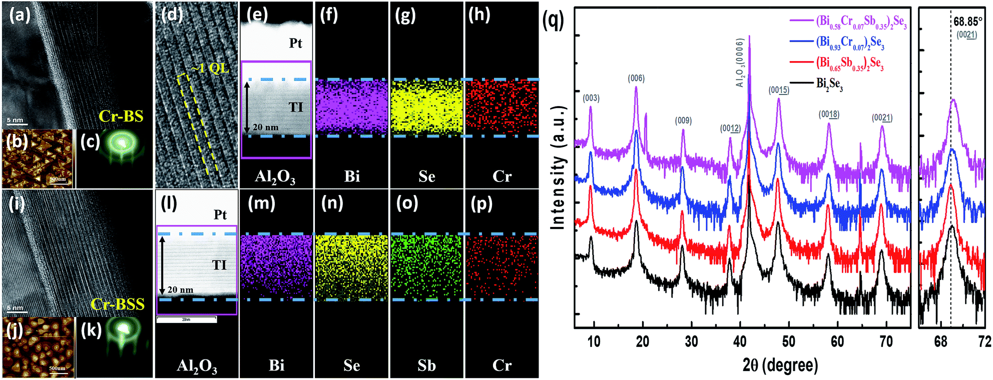 | ||
| Fig. 1 (a–q) HRTEM, AFM, RHEED, EDS mapping images and XRD of (Bi1−xyCrySbx)2Se3: (a–h) Cr-doped Bi2Se3 (Cr-BS), (i–p) (Cr,Sb)-doped Bi2Se3 (Cr-BSS) MBE films, and (q) X-ray diffraction spectra of the films for (i) x = 0, y = 0; (ii) x = 0.35, y = 0; (iii) x = 0, y = 0.07; (iv) x = 0.35, y = 0.07. Right side shows a zoomed-in view of the (0021) peak. | ||
To investigate the doping effect of Cr and Sb in Bi2Se3, electrical transport properties at room temperature (RT) were measured. Fig. 2(a)–(c) and (d)–(f) show the Sb concentration-dependent carrier density (N2D), sheet resistance (Rs), dimensionless conductivity (kFl), and mean free path l for (Bi1−xSbx)2Se3 and Cr-doped (Bi1−xSbx)2Se3 films, respectively. Fig. 2(a) shows the results obtained from the Hall effect measurement. Below x = 0.35, the carrier density reached the minimum (1.154 × 1013 cm−2), and it rapidly increased for x = 0.4. The same was observed as Rs increased to ∼4 kΩ. Fig. 2(b) shows that kFl gradually diminished as x increased, where kFl = σ/(e2/h), σ is sheet conductance, kF is the Fermi wave vector, and l is the mean-free path. At a concentration of x = 0.35, where kFl is ∼6.635 ≥ 1, the material remained metallic, implying transport well within the quantum diffusive regime.
 | ||
| Fig. 2 Transport properties for (Bi1−xSbx)2Se3 and Cr-doped (Bi1−xSbx)2Se3 with different x measured at room temperature: ((a and d)) carrier density (solid squares, left axis) and sheet resistance (open circle, right axis) vs. x, ((b and e)) kFl vs. x, and ((c and f)) mean free path l vs. x. | ||
Therefore, the maximum Sb-doping concentration was fixed at x = 0.35 in studying the (Cr,Sb)-doped Bi2Se3 system. One notable feature in Fig. 2(d) is that the carrier density dropped from 9.36 × 1013 cm−2 to 6.26 × 1012 cm−2 at x = 0.35. This indicates a shift of EF towards CBM and lower carrier density in the Cr–Bi2Se3 system. This is due to the Sb-doping and has not previously been observed. The transport properties were further analyzed by calculating kFl as shown in Fig. 2(e). Rs increased up to ∼23 kΩ, and kFl reached ∼1.13 at x = 0.35 (kFl ∼2 at 2 K. See Fig. S2†). According to Maryam Zhang et al.,20 heavy doping of Sb into Bi2Se3 (x = 0.8) could induce topological phase transition (TPT), owing to the smaller SOC strength of Sb. This critical concentration was verified by transport measurement, where metal-insulator transition occurred at kFl ≤ 1, which is consistent with the Ioffe–Regel criterion.20,21 This shows kFl > 1, implying that the material remained a topological nontrivial system.
Subsequently, magnetoconductivity (MC) was performed at 2 K to elucidate the effect of Sb-doping on the TRS breaking phenomenon in Cr–Bi2Se3. As shown in Fig. 3(a), pure Bi2Se3 and Sb-doped Bi2Se3 exhibited negative MC, which is a typical behavior of high SOC materials, called weak anti-localization (WAL). Crossover from negative MC to positive was observed when Cr was doped to TI, as indicated by a sharp positive cusp in the low-field region. This phenomenon is characteristic of weak localization (WL) and could be attributed to the magnetic-dopant induced magnetization in the sample.13,22
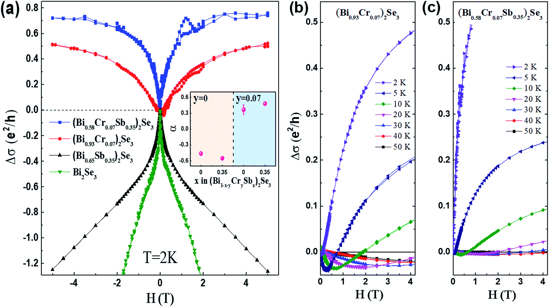 | ||
| Fig. 3 (a) Magnetoconductivity measured at 2 K. Lower half shows that the pure Bi2Se3 and (Bi,Sb)2Se3 films possess typical negative MC, a characteristic of WAL. The upper half shows the positive MC of Cr-doped Bi2Se3 that was increased by doping Sb impurities. (b) and (c) show the MC of Cr-doped Bi2Se3 and (Cr,Sb)-doped Bi2Se3 films, respectively, measured at various temperature. | ||
Interestingly, Sb-doped (Bi,Cr)2Se3 (at x = 0.35) exhibited enhanced positive MC, as indicated by larger values of Δσ. According to the MC formula derived for massive Dirac fermions, crossover from WAL to WL is expected as a result of surface the gap opening Δ, which is tunable by the TRS breaking gap size and the position of EF.23–25 WL will dominate over WAL as the Δ/EF ratio increases. The MC curves of all samples shown in Fig. 3(a) can be well fitted using the Hikami–Larkin–Nagaoka (HLN) formula (See Fig. S3†). The Fig. 3(a) shows the extracted alpha α for various samples. The non-Cr-doped TIs (y = 0) exhibited α values around −0.5, which is the typical value for gapless topological insulators. However, transition from negative to positive α was observed when TI was doped with Cr (y = 0.07), where the maximum value ∼0.5 was observed for the Sb-doped Cr-BS. Such a transition might indicate the onset of ferromagnetism in Cr-doped TIs. Notably, α of Cr-BS tended to increase with Sb-doping. As shown in the Hall measurement, Cr-BSS exhibited N2D that was significantly lower than that of the other samples, indicating that EF was located inside the bulk gap. Large reduction of N2D would lead to higher Δ/EF, resulting in larger values of α. However, the value of the extracted α for Cr–Bi2Se3 was not as expected, as it was quite large, namely, around 0.4. Such a large α obtained in high carrier concentration Cr–Bi2Se3 may indicate the bulk states contribution to the positive MC, which is a characteristic of field induced magnetization resulting in negative magnetoresistance.22 As the EF of Cr-BSS is located inside the bulk electronic bandgap, the positive MC is better described by HLN for this sample. For the subsequent measurements, Cr-BSS was used for studying magnetism at this surface-dominated regime.
The dominance of positive MC in (Cr,Sb)-doped Bi2Se3 was further investigated by studying the temperature-dependent MC measured from 2 K to 50 K. Qualitatively, both Cr-BS and Cr-BSS exhibited MC with similar temperature evolution, as shown in Fig. 3(b) and (c). The low-field MC was negative at high temperature, whereas it was positive as the magnetic field increased. This trend demonstrated the phenomenon of field induced magnetization of the sample, relating to the enhancement of the degree of TRS breaking at high magnetic field.22 The main difference between Cr–Bi2Se3 and (Cr,Sb)-doped Bi2Se3 was that positive MC was still observed at high field and persisted up to 30 K for (Cr,Sb)-doped Bi2Se3. By contrast, considerably stronger suppression of positive MC in Cr–Bi2Se3 was observed, where crossover of positive to negative MC occurred slightly above 10 K.
To investigate the underlying mechanism for the enhancement of positive MC in Sb-doped (Cr,Bi)2Se3, the Hall resistance Rxy was measured for the samples with varying Sb content. In Fig. 4(a), Rxy is plotted as a function of external magnetic field. All samples exhibited negative dRxy/dH in the high-field linear region, indicating the n-type carrier as the major transport carrier in this system. The high-field slope increased as the Sb content increased, which is consistent with previous data, where Sb-doping could reduce the carrier density in Cr–Bi2Se3. Furthermore, the low-field region exhibited nonlinear Rxy, resembling the anomalous Hall contribution of magnetic materials. For a magnetic material, the Hall resistance is given by26
| Rxy = RNH + RAHM(T,H) |
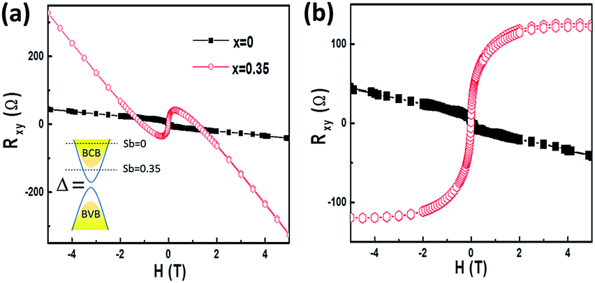 | ||
| Fig. 4 (a) Field-dependent Rxy of Cr-BSS and Cr-BS films. Inset shows the proposed schema of the band dispersion of Cr–Bi2Se3, where the TRS is broken and opens a surface gap Δ. The dashed line indicates the location of EF before and after Sb-doping.; (b) Ferromagnetic ordering is observed after the background subtraction (ordinary high-field linear Hall curve) for the Cr-BSS sample (open symbols). | ||
Finally, ARPES measurements were performed to study the change of electronic structure in the (Bi1−x−yCrySbx)2Se3 system. Fig. 5 shows the ARPES and the corresponding energy distribution curves (EDCs) (bottom panel) for the Bi2Se3, (Bi0.65Sb0.35)2Se3, (Bi0.93Cr0.07)2Se3 and (Bi0.58Cr0.07Sb0.35)2Se3. Topological surface state is clearly observed in pure Bi2Se3 and (Bi,Sb)2Se3, as shown in Fig. 5(a) and (b). Sb-doped Bi2SeS exhibited a similar dispersion except that the position of EF was shifted toward the Dirac point. Fig. 5(c) shows the expected surface gap opening owing to Cr-doping, which is consistent with previous studies.13,21,23 The extracted surface gap from ARPES was around 0.07 eV. Interestingly, when Sb was doped into (Cr,Bi)2Se3, the surface gap increased to ∼0.15 eV (Fig. 5(d)). This shows the consistency of magneto-transport measurement. In magneto-transport measurement, the Sb-doped (Cr,Bi)2Se3 enhanced magnetism, as indicated by the positive MC and anomalous Hall results. Such a surface-gap opening enhanced by a non-magnetic dopant in Cr–Bi2Se3 was also reported by Chang et al.,13 where the gap size increased with decreasing electron donation resulting from Mg-doping. According to their first-principle calculations and STM analysis, the charging of electrons into the Cr multimers might result in the suppression of ferromagnetism.13 The charged/discharged electrons could cause significant structural distortion that may weaken/strengthen the ferromagnetic coupling of the neighboring Cr ions.13 The Sb-doped Cr–Bi2Se3 system of the present study exhibited even lower EF, and this could account for the enhancement of the surface gap opening in this quaternary compound.
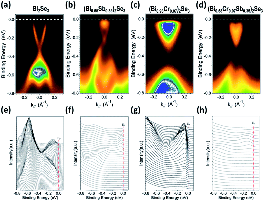 | ||
| Fig. 5 ARPES gray-scale band maps (a–d) and the corresponding EDCs (e–h) for the Bi2Se3, (Bi0.65Sb0.35)2Se3, (Bi0.93Cr0.07)2Se3, and (Bi0.58Cr0.07Sb0.35)2Se3, respectively, taken at 80 K. | ||
Even though the exact mechanism for the codoping-enhanced surface gap and magnetism is presently unclear, this study demonstrates a versatile method in which the MBE-grown, Sb-doped Cr–Bi2Se3 exhibits great potential for gate-tuning of transport and magnetism. In comparison to other Bi2Se3-based quaternary magnetic systems, such as Mg-doped (Cr,Bi)2Se3 and Bi1.84−xFe0.16CaxSe3,11,13 the results of this study more promising, as lower carrier densities (∼6 × 1012 cm−2, i.e., below bulk conduction band) and enhanced ferromagnetism with pure phase were obtained.
Conclusions
The doping effect of Cr and Sb in epitaxy Bi2Se3 thin films was systematically studied by structural, electrical, and magnetic properties measurements. The results demonstrated that owing to the Sb-doping, the films of (Cr,Sb)-doped Bi2Se3 exhibited enhanced weak localization-like positive magnetoconductivity and ferromagnetism. Large tunability in electrical transport and magnetic properties could be the main ingredients for future field-effect and applications of spintronic devices.Conflicts of interest
There are no conflicts to declare.Acknowledgements
This research was supported by the Ministry of Science and Technology of Taiwan, Republic of China, under contract MOST 103-2119-M-006-015-MY3 and 104-2119-M-006-018-MY3. The support of the Headquarters of University Advancement at NCKU, which is sponsored by the Ministry of Education, Taiwan ROC, is also gratefully acknowledged. The National Synchrotron Radiation Research Center (NSRRC) is operated under the Ministry of Science and Technology of Taiwan.Notes and references
- L. He, X. Kou and K. L. Wang, Review of 3D topological insulator thin-film growth by molecular beam epitaxy and potential applications, Phys. Status Solidi RRL, 2013, 7(1–2), 50–63 CrossRef CAS.
- D. Kong and Y. Cui, Opportunities in chemistry and materials science for topological insulators and their nanostructures, Nat. Chem., 2011, 3, 845–849 CrossRef CAS PubMed.
- M. Z. Hasan and C. L. Kane, Colloquium: Topological insulators, Rev. Mod. Phys., 2010, 82, 3045 CrossRef CAS.
- J. E. Moore, The birth of topological insulators, Nature, 2010, 464, 194–198 CrossRef CAS PubMed.
- X. L. Qi and S. C. Zhang, Rev. Topological insulators and superconductors, Mod. Phys., 2011, 83, 1057–1110 CrossRef CAS.
- H. Zhang, C. X. Liu, X. L. Qi, X. Dai, Z. Fang and S. C. Zhang, Topological insulators in Bi2Se3, Bi2Te3 and Sb2Te3 with a single Dirac cone on the surface, Nat. Phys., 2009, 5, 438–442 CrossRef CAS.
- C. Z. Chang, J. Zhang, X. Feng, J. Shen, Z. Zhang, M. Guo, K. Li, Y. Ou, P. Wei, L. L. Wang, Z. Q. Ji, Y. Feng, S. Ji, X. Chen, J. Jia, X. Dai, Z. Fang, S. C. Zhang, K. He, Y. Wang, L. Lu, X. C. Ma and Q. K. Xue, Experimental Observation of the Quantum Anomalous Hall Effect in a Magnetic Topological Insulator, Science, 2013, 340, 167 CrossRef CAS PubMed.
- J. G. Checkelsky, R. Yoshimi, A. Tsukazaki, K. S. Takahashi, Y. Kozuka, J. Falson, M. Kawasaki and Y. Tokura, Trajectory of the anomalous Hall effect towards the quantized state in a ferromagnetic topological insulator, Nat. Phys., 2014, 10, 731–736 CAS.
- C. Z. Chang, W. Zhao, D. Y. Kim, H. Zhang, B. A. Assaf, D. Heiman, S. C. Zhang, C. Liu, M. H. W. Chan and J. S. Moodera, High-precision realization of robust quantum anomalous Hall state in a hard ferromagnetic topological insulator, Nat. Mater., 2015, 14, 473–477 CrossRef CAS PubMed.
- Y. L. Chen, J. H. Chu, J. G. Analytis, Z. K. Liu, K. Igarashi, H. H. Kuo, X. L. Qi, S. K. Mo, R. G. Moore, D. H. Lu, M. Hashimoto, T. Sasagawa, S. C. Zhang, I. R. Fisher, Z. Hussain and Z. X. Shen, Massive Dirac Fermion on the Surface of a Magnetically Doped Topological Insulator, Science, 2010, 329, 659 CrossRef CAS PubMed.
- H. Li, Y. R. Song, M. Y. Yao, F. Zhu, C. Liu, C. L. Gao, J. F. Jia, D. Qian, X. Yao, Y. J. Shi and D. Wu, Carrier density dependence of the magnetic properties in iron-doped Bi2Se3 topological insulator, J. Appl. Phys., 2013, 113, 043926 CrossRef.
- J. M. Zhang, W. Zhu, Y. Zhang, D. Xiao and Y. Yao, Tailoring Magnetic Doping in the Topological Insulator Bi2Se3, Phys. Rev. Lett., 2012, 109, 266405 CrossRef PubMed.
- C. Z. Chang, P. Tang, Y. L. Wang, X. Feng, K. Li, Z. Zhang, Y. Wang, L. L. Wang, X. Chen, C. Liu, W. Duan, K. He, X. C. Ma and Q. K. Xue, Chemical-Potential-Dependent Gap Opening at the Dirac Surface States of Bi2Se3 Induced by Aggregated Substitutional Cr Atoms, Phys. Rev. Lett., 2014, 112, 056801 CrossRef PubMed.
- W. Xu, T.-S. Lim, H.-K. Seo, S.-Y. Min, H. Cho, M.-H. Park, Y.-H. Kim and T.-W. Lee, N-Doped Graphene Field-Effect Transistors with Enhanced Electron Mobility and Air-Stability, Small, 2014, 10(10), 1999–2005 CrossRef CAS PubMed.
- W. Xu, L. Wang, Y. Liu, S. Thomas, H.-K. Seo, K.-I. Kim, K. S. Kim and T.-W. Lee, Controllable n-Type Doping on CVD-Grown Single- and Double-Layer Graphene Mixture, Adv. Mater., 2015, 27(9), 1619–1623 CrossRef CAS PubMed.
- D. Kong, Y. Chen, J. J. Cha, Q. Zhang, J. G. Analytis, K. Lai, Z. Liu, S. S. Hong, K. J. Koski, S. K. Mo, Z. Hussain, I. R. Fisher, Z.-X. Shen and Y. Cui, Ambipolar field effect in the ternary topological insulator (BixSb1–x)2Te3 by composition tuning, Nat. Nanotechnol., 2011, 6, 705–709 CrossRef CAS PubMed.
- J. Zhang, C. Z. Chang, Z. Zhang, J. Wen, X. Feng, K. Li, M. Liu, K. He, L. Wang, X. Chen, Q. K. Xue, X. Ma and Y. Wang, Band structure engineering in (Bi1−xSbx)2Te3 ternary topological insulators, Nat. Commun., 2011, 2, 574 CrossRef PubMed.
- M. Brahlek, N. Bansal, N. Koirala, S. Y. Xu, M. Neupane, C. Liu, M. Z. Hasan and S. Oh, Topological-Metal to Band-Insulator Transition in (Bi1−xInx)2Se3 Thin Films, Phys. Rev. Lett., 2012, 109, 186403 CrossRef PubMed.
- Y. H. Liu, C. W. Chong, W. C. Chen, J. C. A. Huang, C. M. Cheng, K. D. Tsuei, Z. Li, H. Qiu and V. V. Marchenkov, Robust topological insulator surface state in MBE grown (Bi_{1−x}Sb_x)_2Se_3, arXiv, 2016, vol. 1611, p. 08395.
- C. Zhang, X. Yuan, K. Wang, Z. G. Chen, B. Cao, W. Wang, Y. Liu, J. Zou and F. Xiu, Observations of a Metal–Insulator Transition and Strong Surface States in Bi2−xSbxSe3 Thin Films, Adv. Mater., 2014, 26, 7110–7115 CrossRef CAS PubMed.
- M. Salehi, H. Shapourian, H. Koirala, M. J. Brahlek, J. Moon and S. Oh, Finite-Size and Composition-Driven Topological Phase Transition in (Bi1−xInx)2Se3 Thin Films, Nano Lett., 2016, 16, 5528–5532 CrossRef CAS PubMed.
- M. Liu, J. Zhang, C. Z. Chang, Z. Zhang, X. Feng, K. Li, K. He, L. l. Wang, X. Chen, X. Dai, Z. Fang, Q. K. Xue, X. Ma and Y. Wang, Crossover between Weak Antilocalization and Weak Localization in a Magnetically Doped Topological Insulator, Phys. Rev. Lett., 2012, 108, 036805 CrossRef PubMed.
- H. Z. Lu, J. Shi and S. Q. Shen, Competition between Weak Localization and Antilocalization in Topological Surface States, Phys. Rev. Lett., 2011, 107, 076801 CrossRef PubMed.
- H. Z. Lu and S. Q. Shen, Finite-Temperature Conductivity and Magnetoconductivity of Topological Insulators, Phys. Rev. Lett., 2014, 112, 146601 CrossRef PubMed.
- G. Zheng, N. Wang, J. Yang, W. Wang, H. Du, W. Ning, Z. Yang, H. Z. Lu, Y. Zhang and M. Tian, Weak localization effect in topological insulator micro flakes grown on insulating ferrimagnet BaFe12O19, Sci. Rep., 2016, 6, 21334 CrossRef CAS PubMed.
- J. Zhang, C. Z. Chang, P. Tang, Z. Zhang, X. Feng, K. Li, L. L. Wang, X. Chen, C. Liu, W. Duan, K. He, Q. K. Xue, X. Ma and Y. Wang, Topology-Driven Magnetic Quantum Phase Transition in Topological Insulators, Science, 2013, 339, 1582 CrossRef CAS PubMed.
- J. G. Checkelsky, J. Ye, Y. Onose, Y. Iwasa and Y. Tokura, Dirac-fermion-mediated ferromagnetism in a topological insulator, Nat. Phys., 2012, 8, 729–733 CrossRef CAS.
Footnotes |
| † Electronic supplementary information (ESI) available: The reader is referred to supplementary material for the complete data of this study. Fig. S1 shows the AFM images and the RHEED pattern of various samples. Sheet resistance and fitting of MC curves using Hikami–Larkin–Nagaoka formula for Cr-BS and Cr-BSS samples measured at 2 K are shown in Fig. S2 and S3 respectively. Fig. S4 shows the out-of-plane magnetic properties of samples measured by SQUID magnetometer at 2 K. See DOI: 10.1039/c7ra08201k |
| ‡ Y. Tung and C. W. Chong contributed equally to this work. |
| This journal is © The Royal Society of Chemistry 2017 |