
 Open Access Article
 This Open Access Article is licensed under a Creative Commons Attribution-Non Commercial 3.0 Unported Licence
Arsenene/Ca(OH)2 van der Waals heterostructure: strain tunable electronic and photocatalytic properties†
Xiao-Hua Li a,
Bao-Ji Wang*a,
Xiao-Lin Caia,
Wei-Yang Yua,
Li-Wei Zhanga,
Guo-Dong Wanga and
San-Huang Ke*b
a,
Bao-Ji Wang*a,
Xiao-Lin Caia,
Wei-Yang Yua,
Li-Wei Zhanga,
Guo-Dong Wanga and
San-Huang Ke*b
aSchool of Physics and Electronic Information Engineering, Henan Polytechnic University, Jiaozuo 454000, China. E-mail: wbj@hpu.edu.cn
bMOE Key Labortoray of Microstructured Materials, School of Physics Science and Engineering, Tongji University, Shanghai, 200092, China. E-mail: shke@tongji.edu.cn
First published on 15th September 2017
Abstract
Vertical stacking of two-dimensional materials has recently emerged as an exciting method for the design of novel electronic and optoelectronic devices. In this work, we investigate the structural, electronic, and potential photocatalytic properties of arsenene/Ca(OH)2 van der Waals (vdW) heterostructures using first-principles calculations. It is found that all of the heterostructures are semiconductors with indirect band gaps and present similar electronic properties, almost irrespective of the stacking arrangement. However, among these heterostructures, the β-stacking heterostructure is found to be the most stable and its band gap and band edge position can be tuned by biaxial strain. In particular, comparing the band edge positions with the redox potentials of water shows that the strained β-stacking arsenene/Ca(OH)2 vdW heterostructure is a potential photocatalyst for water splitting. Meanwhile, this heterostructure exhibits significantly improved photocatalytic properties under visible-light irradiation by the calculated optical absorption spectra. Our findings provide a detailed understanding of the physical properties of arsenene/Ca(OH)2 vdW heterostructures and a new way to improve the design of photocatalysts for water splitting.
1 Introduction
The family of two-dimensional (2D) materials has grown appreciably since the first isolation of graphene. Lots of graphene-like 2D materials, such as boron nitride,1,2 transition metal dichalcogenides (TMDCs),3 phosphorene,4–6 and others7–10 have been widely studied due to their remarkable physical properties and numerous promising applications.8,9 However, the studies on single layer alkaline-earth-metal hydroxides (AEMHs) (i.e., Ca(OH)2 and Mg(OH)2) are sparse and have only started very recently.11,12 Aierken et al. investigated the structural, electronic, magnetic, vibrational, and mechanical properties of monolayer Ca(OH)2 by first-principles calculations. The results show that Ca(OH)2 can be isolated in monolayer form and it is a direct bandgap semiconductor independent of the number of layers.12 Besides, monolayer gray arsenic (arsenene), a new elemental 2D semiconducting material with buckled honeycomb lattice, has been recently proposed and was predicted to be kinetically very stable based on the theoretical calculations.13–16 It is also found that the arsenene is an indirect-band-gap semiconductor and undergoes an indirect-to-direct band-gap and semiconducting-to-metallic transitions under external electric fields or strains.13,16In addition, it is worth noting that these 2D materials offer a platform that allows creation of van der Waals (vdW) heterostructures comprised of at least two types of chemically different 2D materials, where the one layered 2D material are stacked on the other and held together by vdW forces.17,18 Such stacks are very different from the traditional 3D semiconductor heterostructures, as each layer acts simultaneously as the bulk material and the interface, reducing the amount of charge displacement within each layer. As a consequence, beyond being novel atomic-thick materials, vdW heterostructures have received considerable attention. Recently, a great deal of vertically-stacked vdW heterostructures have been realized experimentally and utilized to create electronic and optoelectronic devices with novel physical properties and distinctive capabilities.19–21 At the same time, many theoretical researchers have also shifted their focus from monocomponent systems to vdW heterostructures. The work by Su et al. showed that the indirect bandgap of arsenene/MoS2 heterostructures is tunable by changing the interlayer distance and increase with the increasing interlayer distance.22 A theoretical study23 demonstrated that the GaS/Ca(OH)2 heterobilayer is a type-II heterojunction where spatially separated charge carriers can be formed. The optical spectra of different stacking types exhibit distinct properties. Our previous work suggests that arsenene/GaS heterostructure is a promising photocatalyst for water splitting and its electronic properties can be continuously tuned by external strain.24 All these findings suggest that stacking 2D materials into vdW heterostructures provides an effective way to design novel artificial materials with special characteristics. This motivates us to consider whether arsenene and Ca(OH)2 monolayer can form a stable arsenene/Ca(OH)2 (A/C) vdW heterostructure, and what interesting electronic or optical properties it can provide. In this work, by performing first-principles calculations, we predict a strain dependence of the electronic and optical properties of the A/C vdW heterostructures. Band edge alignments of the A/C heterostructures under various strains are investigated with respect to water oxidation and reduction potentials. Our results reveal that A/C heterostructures could be a promising material for visible light photocatalysis and electronic and optoelectronic devices.
2 Computational methods
All the density-functional theory (DFT) calculations are performed with the Vienna Ab initio Simulation Package (VASP) code.25 The projector-augmented wave (PAW) method is applied to describe the electron–ion interactions.26 The electron exchange and correlation are treated by the Perdew–Burke–Ernzerhof (PBE) functional27 within the generalized gradient approximation (GGA) formalism.28 To correct the well-known underestimation of bandgap in DFT/PBE calculations, the hybrid Heyd–Scuseria–Ernzerhof (HSE06)29,30 is adopted. The DFT-D2 correction of Grimme31 is used to describe the interlayer vdW interaction, which has been evidenced to give a reliable description for various vdW heterostructure systems.22,32–35 Plane waves with a kinetic energy cutoff of 500 eV are used to expand the wave functions and the self-consistent convergence accuracy was set at 10−5 eV per atom. The Brillouin zone (BZ) is sampled by a 48 × 48 × 1 Monkhorst–Pack k-point mesh36 for the PBE calculations, and an 18 × 18 × 1 mesh for the more expensive HSE06 calculations. A vacuum spacing of larger than 25 Å is adopted to eliminate the spurious interactions between the periodic imagines. Our test calculations show that the k-point grid and vacuum spacing adopted are sufficient to obtain well converged results. The lattice vectors and atomic positions are fully relaxed by minimizing the quantum mechanical stresses and forces. The atomic structures are optimized until the Hellmann–Feynman forces acting on each atom are less than 0.01 eV Å−1 within the conjugate gradient algorithm.3 Results and discussions
As a test for our approach and parameterization, we first calculate the structural parameters of pristine arsenene and Ca(OH)2 monolayers. The optimized atomic structures of the two monolayers are shown in Fig. 1(a) and (c), respectively. Their lattice constants are almost equal to each other: 3.61 and 3.58 Å for arsenene and Ca(OH)2, respectively. The bond length in arsenene is 2.51 Å, while in Ca(OH)2 monolayer the bond lengths of Ca–O and O–H bonds are 2.36 Å and 0.97 Å, respectively (see Table 1). The band structures of arsenene and Ca(OH)2 monolayers are calculated with the PBE and HSE06 functionals and presented in Fig. 1(b) and (d), respectively. The results show that arsenene monolayer is semiconductor with an indirect band gap of 1.60/2.21 eV given by PBE/HSE06. The valence band maximum (VBM) at Γ-point comprises mainly the px and py states of As atoms, while the conduction band minimum (CBM) located at the halfway of Γ–M comprises mainly the s and p states of As atoms. Differing from arsenene monolayer, Ca(OH)2 monolayer has a direct bandgap of 3.67/5.17 eV obtained by the PBE/HSE06 calculation, as shown in Fig. 1(d). Both the VBM and CBM reside at Γ-point in the BZ. The Frontier valence band states originate from the px and py states of the O atom, however, the states near the CBM are mostly from the s states of Ca atoms and s and pz states of O atoms (see Fig. 1(d) (right plane)). All these structural and electronic properties of arsenene and Ca(OH)2 monolayers agree well with previous studies.16,23,37 One should note that the more accurate HSE06 band structure can be basically obtained by upshifting/downshifting the conduction/valence bands of the PBE bands, indicating the band dispersions given by the PBE functional are still reasonable though the bandgap is too small.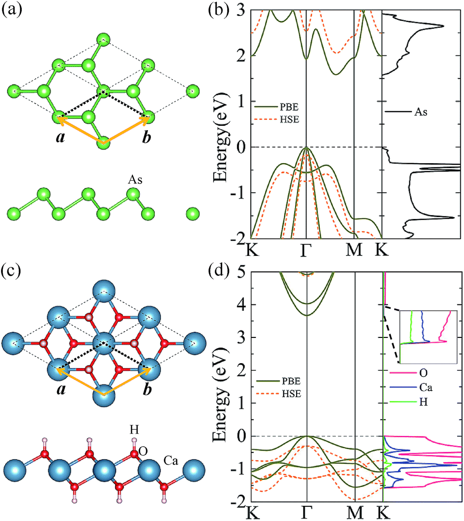 | ||
| Fig. 1 (color online) Top and side views of (a) arsenene and (c) Ca(OH)2 monolayers. The orange rhombus indicates the unit cell. The arsenic (As), calcium (Ca), oxygen (O), and hydrogen (H) atoms are presented by green, blue, red, and white balls, respectively. The calculated band structures of monolayer arsenene (b) and Ca(OH)2 (d) solid dark yellow lines present the PBE results while dashed orange lines present the HSE06 results. The corresponding projected density of states from the PBE calculation are given in (b) and (d) (right plane), respectively. | ||
| a = b (Å) | dAs–As (Å) | dH–O (Å) | dCa–O (Å) | Eb (meV per unit) | EPBEg (eV) | EHSEg (eV) | |
|---|---|---|---|---|---|---|---|
| Arsenene | 3.61 | 2.51 | 1.60 | 2.21 | |||
| Ca(OH)2 | 3.58 | 0.97 | 2.36 | 3.67 | 5.17 | ||
| α-Stacking | 3.60 | 2.51 | 0.97 | 2.37 | −166 | 1.59 | 2.11 |
| β-Stacking | 3.60 | 2.51 | 0.97 | 2.37 | −171 | 1.60 | 2.22 |
| γ-Stacking | 3.60 | 2.51 | 0.97 | 2.36 | −163 | 1.55 | 2.15 |
We consider three high-symmetry stacking structures named as α-, β- and γ-stacking, as depicted in Fig. 2(a–c). In the α-stacking, As atoms of the two sublattices are located on top of OH groups, while in the β (γ)-stacking one As sublattice is positioned on top of Ca atoms and the other is on top of upper (lower) OH group. To compare the relative stability of these heterostructures, we calculate their interface binding energies, Eb = EA/C − EA − EC, where EA/C, EA, and EC represent total energies of the A/C heterostructure, arsenene and Ca(OH)2 monolayer, respectively. By this definition, a lower Eb value means better stability of the heterostructure. As shown in Table 1, the predicted Eb values per unit cell for the three heterostructures are very close to each other and follow the order of Eβ (−171 meV) < Eα (−166 meV) < Eγ (−163 meV), which means that the three considered heterostructures possess very similar stability, although the β-stacking one is the most stable one. Moreover, the lattice parameters, bond lengths, and interlayer distances of the three A/C heterostructures are almost identical, resulting in very similar band structures (see Fig. 3(a)) and strain tunable electronic properties (see ESI: Fig. S1†). Similar behavior is also found in arsenene/MoS2 heterostructures22 and germanene/BeO heterostructures.38 Thus, in the following sections, only the most stable A/C heterostructures with β configuration is focused and discussed.
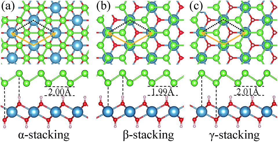 | ||
| Fig. 2 (color online) Top (up panel) and side (down panel) views of different possible stacking configurations for the A/C heterostructures: (a) α-stacking, (b) β-stacking, and (c) γ-stacking. The optimized interlayer distances are indicated. | ||
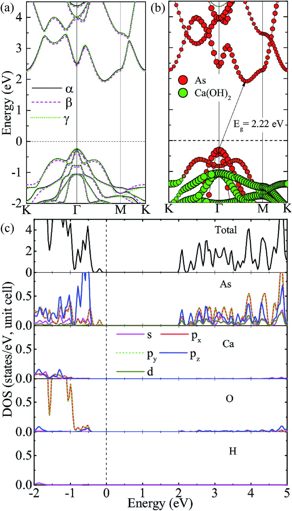 | ||
| Fig. 3 (color online) (a) Band structures of the three A/C heterostructures given by the hybrid HSE06 functional. (b) and (c) Projected band structure of β-stacking A/C heterostructure and the corresponding total and partial density of states obtained from the HSE06 functional. | ||
We first investigate the electronic properties of the A/C vdW heterostructure. The projected band structure given by the HSE06 calculation is illustrated in Fig. 3(b), in which the circles filled by red and green indicate the contributions from the arsenene and Ca(OH)2 layers, respectively. Obviously, the A/C heterostructure is a semiconductor with an indirect bandgap of 2.22 eV and its CBM and VBM are all mainly contributed from arsenene, indicating the formation of type-I heterostructure is formed. To show more details, the total and partial density of states (PDOS) are also plotted in Fig. 3(c). One can see that the states around VBM are mainly dominated by the p(x,y) states of As atoms, whereas the dominant contributions to the CBM originate from lone-pair pz states of As atoms, which induces the formation of the π-like states in the interlayer region and are beneficial to bring the arsenene and Ca(OH)2 layers together.22,39
To analyze the charge transfer between the arsenene and Ca(OH)2 layers, in Fig. 4(a) we plot the deformation charge density (DCD) Δρ(z) of the heterostructure along the z direction normal to the surface as  , where ρA/C(x,y,z), ρA(x,y,z) and ρC(x,y,z) are the charge density at (x,y,z) points in the heterostructure, the pristine arsenene and pristine monolayer Ca(OH)2, respectively. Therefore, positive values indicate charge accumulation while negative values mean charge depletion. One can see that the Ca(OH)2 layer donates electrons to the arsenene layer, which leads to p-doping in Ca(OH)2 and n-doping in arsenene. The isosurface of the DCD is added in Fig. 4(a) as an inset, where the loss and the accumulation of electrons across the interface are directly depicted. The amount of transferred electrons up to z point is given by
 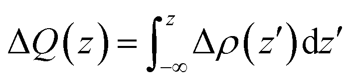 . The results in Fig. 4(a) (right y-axis) show that about 0.017|e| per unit cell is transferred from the Ca(OH)2 to arsenene layer, which is determined by the value of ΔQ(z) at the A/C interface (defined as the plane of zero charge variation as shown in the Δρ(z) curve).40 Fig. 4(b) shows the plane-averaged electrostatic potential along z-direction normal to the surface. The arsenene layer has a deeper potential than that of the Ca(OH)2 layer, driving electrons to move from the Ca(OH)2 layer to arsenene, which can be understood by considering the different electronegativities of the atoms. The potential drop (ΔVA/C) across the bilayer is found to be 4.68 eV. Such a large potential difference implies a strong electrostatic field across the interface, which may significantly influence the carrier dynamics and charge injection if the Ca(OH)2 is served as the electrode. In addition, the excitonic behavior of A/C heterostructure can be quite different from that of the isolated Ca(OH)2 layer as the gradient of the potential across the interface may facilitate the separation of electrons and holes.40
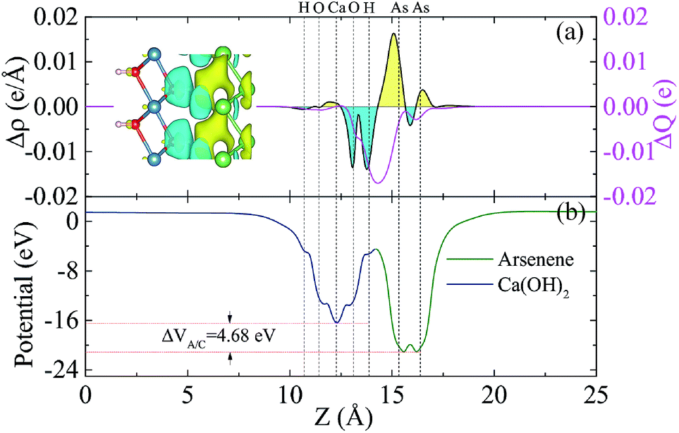 | ||
| Fig. 4 (color online) (a) Plane-averaged charge density difference (black) and the amount of transferred charge ΔQ(z) along the normal direction of the surface (magenta) for the A/C heterostructure. The inset in (a) is the 3D isosurface of the charge density difference. The yellow and cyan areas represent electrons accumulation and depletion, respectively. (b) Potential profile across the interface of the A/C heterostructure. The vertical dotted lines indicate the position of the H, O, Ca, and As atoms in the heterostructure, respectively. The results are from the HSE06 calculations. | ||
Tunability of electronic properties of a material by external control, such as strain, is very beneficial for its applications in nanoelectronics or optoelectronics.41 Here, we consider in-layer biaxial strain effects on the electronic structures of the A/C heterostructure, where the hexagonal unit cell is enlarged or shrunk symmetrically with specific ratios. Thus, 2D-isotropic deformation (ε) is defined as ε = (L − L0)/L0, where L and L0 are the lattice constants for the strained and unstrained structures, respectively. According to this definition, a negative value means a compressive strain, while a positive value indicates a tensile stress. The band-gap evolution given by the vdW-DFT/PBE under various biaxial strains is shown in Fig. 5(a) together with the strain energy. One can see that the bandgap reaches its maximum value (∼1.62 eV) at the strain of about +2% and then decreases with the compressive or tensile strain increasing. Then, the system goes from semiconducting to metallic for strains beyond −10%. We note that DFT/PBE usually underestimates bandgaps of semiconductors because of the lacking of derivative discontinuity in the energy functional. However, our purpose here is to see the trend in bandgap variation under different strains instead of the absolute values of bandgap, therefore the results can still be expected to be meaningful. This justification is also supported by previous calculations using the PBE functional and the HSE06 hybrid functional, showing consistent strain-induced effects on band structures.42
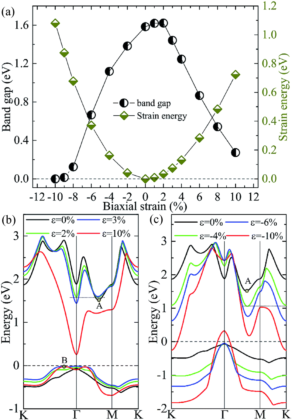 | ||
| Fig. 5 (color online) (a) The bandgap and strain energy calculated by DFT/PBE + vdW as functions of the in-layer biaxial strain for the A/C heterostructure. The evolutions of the highest valence bands and the lowest conduction bands of the A/C heterostructures under various tensile (b) and compressive (c) biaxial strains. | ||
The dependencies of the highest valence and lowest conduction bands on the biaxial strains are shown in Fig. 5(b) and (c), which clearly demonstrate that the size and characteristic of the band-gap is determined by the strain-induced band-energy shifts at different k points. Similar to the HSE06 result, the free-standing heterostructure possesses an indirect bandgap between VBM at Γ point and CBM at k1(0.32, 0, 0) denoted by A in Fig. 5(b) or (c). Under an increasing small tensile strain, the VBM is located at Γ point while the energy of the conduction band bottom at Γ point shifts downwards more rapidly than the original CBM and becomes the new CBM, leading to an indirect–direct (I–D) transition at ε ≃ +2%. When the tensile strain is further increased (ε ≥ +4%), the CBM remains at Γ point, but the k2(0.1, 0.1, 0) denoted by B in Fig. 5(b) evolves gradually into the new VBM, which results in a D–I transition. In this case, the direct bandgaps at Γ point are very close in size to the indirect bandgaps (B–Γ) with a maximum energy difference of 0.07 eV. One can expect that the (quasi-)direct interband transitions at the Γ point improve the optical absorption (see later discussion). On the other hand, when an increasing compressive strain is applied, both the conduction and valence bands tend to shift downwards. The VBM is always located at Γ-point while the conduction band bottom at K point drops faster than A, and becomes equal in energy to A at ε ≃ −4.0%, and eventually becomes the new CBM when ε > −4.0%. Moreover, compressions greater than −10% induce a semiconductor–metal transition, where the bands cross the Fermi level at the K (conduction band) and Γ (valence band) points. It is interesting to note that there are two critical strains, +2.0% and −4.0%, under which degenerate conduction band valleys are created. This behavior would have potential applications for valleytronic devices: quasiparticles with the same energy at different positions in momentum space are less susceptible to phonon scattering.43,44
To check if all the strains considered are within the elastic limit, we calculate the strain energy per atom, Es = (Estrained − Eunstrained)/n, with n being the number of atoms in the unit cell. The results in Fig. 5(a) (right y-axis) show that Es varies smoothly as a quadratic function of the strain, indicating that the system is flexible and all the strains considered are within the elastic limit and, therefore, are fully reversible.
Since the bandgap of the A/C heterostructure are mechanically tunable, it is worthwhile exploring its potential for energy conversion applications, e.g., photocatalytic water splitting. To become a promising photocatalyst for water splitting, a material must satisfy two important criteria: (i) the bandgap of the semiconductor must be at least 1.6–1.7 eV and (ii) the band edges must straddle the redox potential energies of water, i.e., −4.44 eV and −5.67 eV for the hydrogen and oxygen evolution, respectively. Fig. 6 compares the band edge positions of the A/C heterostructure under the tensile biaxial strains considered with the redox potentials of hydrogen evolution (H+/H2) and oxygen evolution (O2/H2O) at pH = 0. As one can see, for the unstrained A/C heterostructure, the energies of the CBM and VBM relative to the vacuum level are −3.43 eV and −5.65 eV, respectively. Clearly, the VBM is unable to drive the oxygen evolution. However, a moderate tensile strain in the range from 1% to 6% reduces the VBM to become lower than the O2/H2O energy, rendering it useful in spontaneous photocatalytic water splitting. In particular, when ε ≃ +4% the bandgaps and band edge levels of the heterostructure become much match to the standard requirements for photocatalytic water splitting, which indicates that better photocatalytic performance might be expected in the A/C heterostructure with 4% tensile strain. Nevertheless, we notice that for the strains smaller than 6% the position of the VBM is very close to the water oxidation potential, implying a low oxidizing power. So a cocatalyst would be helpful to achieving the whole water splitting for this heterostructure.45 In fact, large pH values can make the redox reactions energetically more favorable, since the redox potentials of water increase with increased pH values, shifting the water's redox energy levels (as shown in Fig. 6) upward.46 When the tensile strain is further increased to be higher than 6%, the VBM will be raised above the oxidation potential of O2/H2O (being similar to the case of the unstrained heterostructure), making it unsuitable for water splitting anymore.
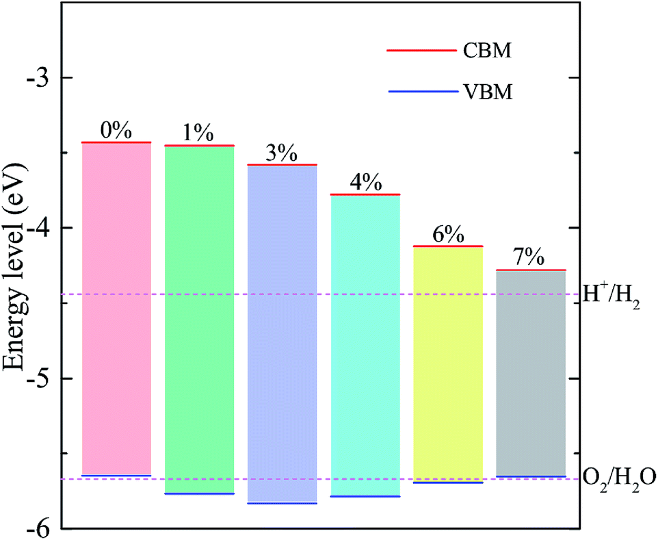 | ||
| Fig. 6 (color online) Band edge positions of the A/C heterostructures under various strains relative to the vacuum level calculated with the HSE06 functional. The CBM (red) and VBM (blue) are presented along with the potentials in electronvolts. The redox potentials (magenta dashed line) of water splitting at pH = 0 are shown for comparison. | ||
In addition to an appropriate bandgap and a suitable band alignment, a catalyst is also required to have outstanding optical adsorption in visible region. To this end, the optical absorbance A(ω) of the A/C heterostructure is determined as A(ω) = ωLImε(ω)/c and the results are shown in Fig. 7, where ω, L, Imε(ω), and c are the frequency of light, the length of the cell in the layer-normal direction, the imaginary part of the dielectric constant, and the speed of light in vacuum, respectively.47 Thereinto, Imε(ω) is calculated using the PBE functional. Following a previous studies,48–50 we compensate for the bandgap underestimation of the PBE functional by a rigid shift of the absorption curves upward by the value of the bandgap difference between the HSE06 and PBE functional. As can be seen, biaxial tensile strain red-shifts the optical spectra at uniform incremental intervals in the range of visible light, leading to significantly enhanced optical absorption in the region of [1.66 eV, 2.86 eV]. This result is related to the aforementioned results that strains cause bandgap reductions and a transition from an indirect to a (quasi-)direct,51 as shown in Fig. 5. Similar behaviors are also found in other two stacking cases although their optical absorptions are weaker than that in the β-stacking A/C heterostructures (see ESI: Fig. S2†). Finally, considering the fact that only few existing materials possess both a (quasi-)direct bandgap and suitable band edge positions, our prediction is important that the strained A/C heterostructures, especially the β-stacking one, is a good potential photocatalyst for water splitting.46
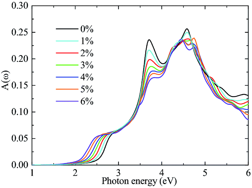 | ||
| Fig. 7 (color online) The optical absorbance spectrum A(ω) of A/C heterostructure under biaxial tensile strain. A(ω) is calculated using the PBE functional followed by a rigid energy shift to take into account the bandgap underestimation of the PBE functional. | ||
4 Conclusions
In summary, by performing first-principles calculations with vdW corrections, we have investigated systematically the geometric and electronic properties of A/C heterostructures. Results show that the A/C heterostructures are formed through vdW and electrostatic interactions, and their binding energies at the optimum spacing are at least −0.16 eV, suggesting the realizability and stability for these three A/C heterostructures. Their geometric parameters and band structures are found to be similar, almost irrespective of the stacking arrangement. The heterostructure with the ground-state configuration is found to be an indirect-band-gap semiconductor with intrinsic type-I band alignment. Also, its electronic properties can be significantly modulated by external uniform strains. An increasing inlayer compressive strain will reduce a semiconductor-to-metal transition, while an increased tensile strain will first increase the bandgap and then rapidly decrease it. In the latter case, degenerate valleys of CBM will be created, which suggests potential applications in valleytronics. Finally, we predict that tensile strains can be applied to tune the band edge positions and optical absorption for a better match with the redox potentials of water and the solar spectrum, such that the A/C vdW heterostructure could become a promising photocatalyst for water splitting.Conflicts of interest
There are no conflicts to declare.Acknowledgements
This research was supported by the National Natural Science Foundation of China (No. 11174220 and 11374226), the Key Scientific Research Project of the Henan Institutions of Higher Learning (No. 16A140009 and 18A140018), the Natural Science Foundation of Henan Province of China (No. 162300410116), the Program for Innovative Research Team of Henan Polytechnic University (No. T2015-3 and T2016-2), the Doctoral Foundation of Henan Polytechnic University (No. B2015-46), and the Open Project of Key Laboratory of Radio Frequency and Micro-Nano Electronics of Jiangsu Province (LRME201601), as well as by the High-performance Grid Computing Platform of Henan Polytechnic University.References
- J. Nakamura, T. Nitta and A. Natori, Phys. Rev. B, 2005, 72, 205429 CrossRef.
- A. Du, S. C. Smith and G. Lu, Chem. Phys. Lett., 2007, 447, 181 CrossRef CAS.
- Y. F. Li, Z. Zhou, S. B. Zhang and Z. F. Chen, J. Am. Chem. Soc., 2008, 130, 16739 CrossRef CAS PubMed.
- L. Li, Y. Yu, G. J. Ye, Q. Ge, X. Ou, H. Wu, D. Feng, X. H. Chen and Y. Zhang, Nat. Nanotechnol., 2014, 9, 372 CrossRef CAS PubMed.
- H. O. H. Churchill and P. Jarillo-Herrero, Nat. Nanotechnol., 2014, 9, 330 CrossRef CAS PubMed.
- H. Liu, A. T. Neal, Z. Zhu, Z. Luo, X. Xu, D. Tomanék and P. D. Ye, Phys. Solid State, 2014, 8, 4033 CAS.
- D. J. Late, B. Liu, J. Luo, A. Yan, M. H. S. S. Ramakrishna, M. Grayson, C. N. R. Rao and V. P. Dravid, Adv. Mater., 2012, 24, 3549 CrossRef CAS PubMed.
- Q. Tang and Z. Zhou, Prog. Mater. Sci., 2013, 111, 1244 CrossRef.
- Q. Tang, Z. Zhou and Z. F. Chen, WIREs Computational Molecular Science, 2015, 5, 360 CrossRef CAS.
- S. L. Zhang, W. H. Zhou, Y. D. Ma, J. P. Ji, B. Cai, S. A. Yang, Z. Zhu, Z. F. Chen and H. B. Zeng, Nano Lett., 2017, 17, 3434 CrossRef CAS PubMed.
- S. Jahangiri and N. J. Mosey, Phys. Chem. Chem. Phys., 2017, 19, 1963 RSC.
- Y. Aierken, H. Sahin, F. Iyikanat, S. Horzum, A. Suslu, B. Chen, R. T. Senger, S. Tongay and F. M. Peeters, Phys. Rev. B, 2015, 91, 245412 CrossRef.
- S. L. Zhang, Z. Yan, Y. F. Li, Z. F. Chen and H. B. Zeng, Angew. Chem., Int. Ed., 2015, 54, 3112 CrossRef CAS PubMed.
- S. L. Zhang, Y. H. Hu, Z. Y. Hu, B. Cai and H. B. Zeng, Appl. Phys. Lett., 2015, 107, 022102 CrossRef.
- S. L. Zhang, M. Q. Xie, F. Y. Li, Z. Yan, Y. F. Li, E. Kan, W. Liu, Z. F. Chen and H. B. Zeng, Angew. Chem., Int. Ed., 2016, 55, 1666 CrossRef CAS PubMed.
- C. Kamal and M. Ezawa, Phys. Rev. B, 2015, 91, 085423 CrossRef.
- K. S. Novoselov, A. Mishchenko, A. Carvalho and A. H. C. Neto, Science, 2016, 353, 461 CrossRef CAS PubMed.
- W. Y. Yu, Z. L. Zhu, S. L. Zhang, X. L. Cai, X. F. Wang, C. Y. Niu and W. B. Zhang, Appl. Phys. Lett., 2016, 109, 103104 CrossRef.
- Z. Wu, Y. Zheng, S. H. Zheng, S. Wang, C. L. Sun, K. Parvez, T. Ikeda, X. Bao, K. Müllen and X. Feng, Adv. Mater., 2016, 29, 1602960 CrossRef PubMed.
- M. S. Long, E. F. Liu, P. Wang, A. Y. Gao, H. Xia, W. Luo, B. G. Wang, J. W. Zeng, Y. J. Fu, K. Xu, W. Zhou, Y. Y. Lv, S. H. Yao, M. H. Lu, Y. F. Chen, Z. H. Ni, Y. M. You, X. A. Zhang, S. Q. Qin, Y. Shi, W. D. Hu, D. Y. Xing and F. Miao, Nano Lett., 2016, 15, 2254 CrossRef PubMed.
- D. Li, X. J. Wang, Q. C. Zhang, L. P. Zou, X. F. Xu and Z. X. Zhang, Adv. Funct. Mater., 2015, 25, 7362 Search PubMed.
- J. Su, L. P. Feng, H. X. Pana, H. C. Lu and Z. T. Liua, Mater. Des., 2016, 96, 257 CrossRef CAS.
- E. Torun, H. Sahin and F. M. Peeters, Phys. Rev. B, 2016, 93, 075111 CrossRef.
- X. H. Li, B. J. Wang, X. L. Cai, L. W. Zhang, G. D. Wang and S. H. Ke, RSC Adv., 2017, 7, 28393 RSC.
- G. Kresse and J. Hafner, Phys. Rev. B, 1993, 47, 558 CrossRef CAS.
- P. E. Blöchl, Phys. Rev. B, 1994, 50, 17953 CrossRef.
- J. P. Perdew, K. Burke and M. Ernzerhof, Phys. Rev. Lett., 1996, 77, 3865 CrossRef CAS PubMed.
- J. P. Perdew, J. A. Chevary, S. H. Vosko, K. A. Jackson, M. R. Pederson, D. J. Singh and C. Fiolhais, Phys. Rev. B, 1992, 46, 6671 CrossRef CAS.
- J. Heyd, G. E. Scuseria and M. Ernzerhof, J. Chem. Phys., 2003, 118, 8207 CrossRef CAS.
- J. Heyd, G. E. Scuseria and M. Ernzerhof, J. Chem. Phys., 2006, 124, 219906 CrossRef.
- S. Grimme, J. Comput. Chem., 2006, 27, 1787 CrossRef CAS PubMed.
- L. Shi, T. S. Zhao, A. Xua and J. B. Xu, J. Mater. Chem., 2016, 4, 16377 RSC.
- Y. Ding and Y. L. Wang, Appl. Phys. Lett., 2013, 103, 043114 CrossRef.
- W. Wei, Y. Dai, C. W. Niu, X. Li, Y. D. Ma and B. B. Huang, J. Mater. Chem. C, 2015, 3, 11548 RSC.
- C. X. Xia, B. Xue, T. X. Wang, Y. T. Peng and Y. Jia, Appl. Phys. Lett., 2015, 107, 193107 CrossRef.
- H. J. Monkhorst and J. D. Pack, Phys. Rev. B, 1976, 13, 5188 CrossRef.
- L. Z. Kou, Y. D. Ma, X. Tan, T. Frauenheim, A. J. Du and S. Smith, J. Phys. Chem. C, 2015, 119, 6918 CAS.
- X. P. Chen, X. Sun, J. K. Jiang, Q. H. Liang, Q. Yang and R. Meng, J. Phys. Chem. C, 2016, 120, 20350 CAS.
- Z. Zhu, J. Guan and D. Tománek, Phys. Rev. B, 2015, 91, 161404 CrossRef.
- Y. Q. Cai, G. Zhang and Y. W. Zhang, J. Phys. Chem. C, 2008, 119, 13929 Search PubMed.
- J. Li, Z. Shan and E. Ma, MRS Bull., 2014, 39, 108 CrossRef CAS.
- X. Peng, Q. Wei and A. Copple, Phys. Rev. B, 2014, 90, 085402 CrossRef.
- H. L. Zeng, J. F. Dai, W. Yao, D. Xiao and X. D. Cui, Nat. Nanotechnol., 2012, 7, 490 CrossRef CAS PubMed.
- X. Y. Han, H. M. Stewart, S. A. Shevlin, C. R. A. Catlow and Z. X. Guo, Nano Lett., 2014, 14, 4607 CrossRef CAS PubMed.
- J. M. Liao, B. S. Sa, J. Zhou, R. Ahuja and Z. M. Sun, J. Phys. Chem. C, 2014, 118, 17594 CAS.
- H. L. Zhuang, M. D. Johannes, M. N. Blonsky and R. G. Hennig, Appl. Phys. Lett., 2014, 104, 022116 CrossRef.
- L. Matthes, P. Gori, O. Pulci and F. Bechstedt, Phys. Rev. B, 2013, 87, 035438 CrossRef.
- H. L. Zhuang and R. G. Hennig, Chem. Mater., 2013, 25, 3232 CrossRef CAS.
- R. Asahi, T. Morikawa, T. Ohwaki, K. Aoki and Y. Taga, Science, 2001, 293, 269 CrossRef CAS PubMed.
- J. Liu, X. B. Li, D. Wang, H. Liu, P. Peng and L. M. Liu, J. Mater. Chem. A, 2014, 2, 6755 CAS.
- D. Kecik, E. Durgun and S. Ciraci, Phys. Rev. B, 2016, 94, 205410 CrossRef.
Footnote |
| † Electronic supplementary information (ESI) available. See DOI: 10.1039/c7ra08029h |
| This journal is © The Royal Society of Chemistry 2017 |